

Page 1
Integrated
Circuit
Systems, Inc.
General Description
Features
ICS9133X
ICS reserves the right to make changes in the device data identified in this publication
without further notice. ICS advises its customers to obtain the latest version of all device
data to verify that any information being relied upon by the customer is current and accurate.
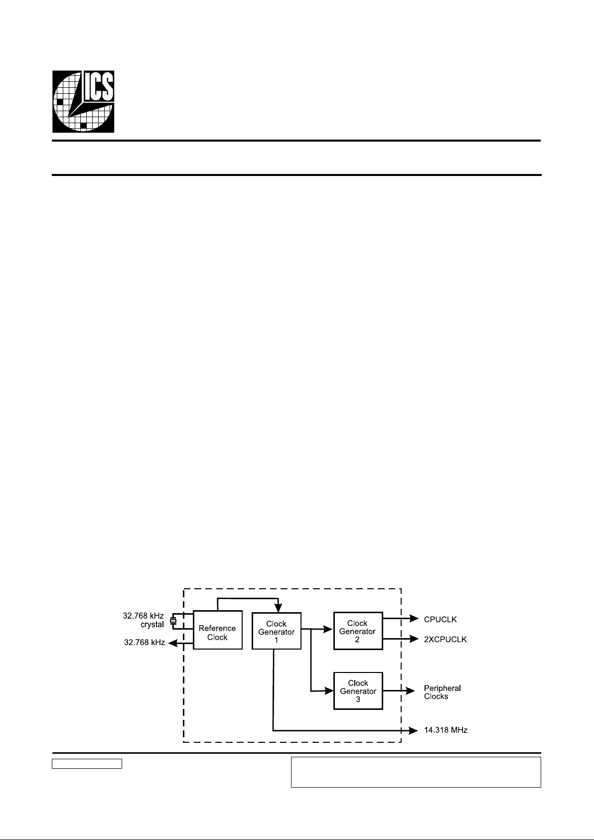
The ICS9133X is designed to generate clocks for all 286, 386,
486, Pentium and RISC-based motherboards, including laptops and notebook computers. T he only e xternal components
required are a 32.768 kHz crystal and decoupling capacitors.
The device generates the 14.318 MHz system c lock, eliminating
the need for a 14.318 MHz crystal. High performance applications
may require high speed clock termination components. The
chip includes three independent clock generators plus the
32.768 kHz reference clock to produce all necessary frequencies,
including real time clock/DRAM refresh, master clock, CPU
clock, twice CPUclock frequency, keyboard clock, floppy
disk controller clock, serial communications clock and bus
clocks. Different frequencies from clock #2 can be selected
using the frequency select pins, but clock #1 will be at 14.318
MHz for all standard versions.
• Single 32.768 kHz crystal generates all PC
motherboard clocks
• Cost-reduced version of popular ICS9132
• Contains internal crystal load capacitors and
feedback bias
• 3 independent clock generators
• Generates CPU clocks from 12.5 to 100 MHz
• Up to 7 output clocks
• Separate VDD for 32 kHz clock
• Output enable tristates outputs
• Power-down options available
• Operates from 3.3V or 5.0V supply
• Operates up to 66 MHz at 3.3V
• Skew controlled 1X and 2X CPU clocks
• 20-pin PDIP or SOIC package
9133X Rev A 052897P
Block Diagram
32 kHz Motherboard Frequency Generator
VDD32 Supply
The ICS9133X has a sep arate power supply for the 32.768
kHz oscillator circuitry. This allows the 32 kHz clock to run
from a battery or other source while the main power to the
chip is disconnected. The VDD32 supply is guaranteed to
operate down to +2.0V, with the clock consuming less than
10µA at +3.3V with the main VDD at 0V.
The frequencies and power-down options in the ICS9133X
are mask programmable. Customer specific masks can be
made and prototypes delivered within 6-8 weeks fr om receipt
of order. Integrated Circuit Systems also of fers standard versions,
such as that described in this data sheet.
Applications
Notebook/Palmtop Computers : The ICS9133X works with
+3V and +5V and a single 32.768 kHz crystal, making it the
ideal solution for generating clocks in portables with minimum
board space. The user can save po wer by using this single part
instead of oscillators or other frequency generators. The
ICS9133X further reduces the current consumption by having
the ability to completely shut down the individual clocks
when not in use, while still maintaining the separately powered
32.768 kHz clock.
Page 2
2
ICS9133X
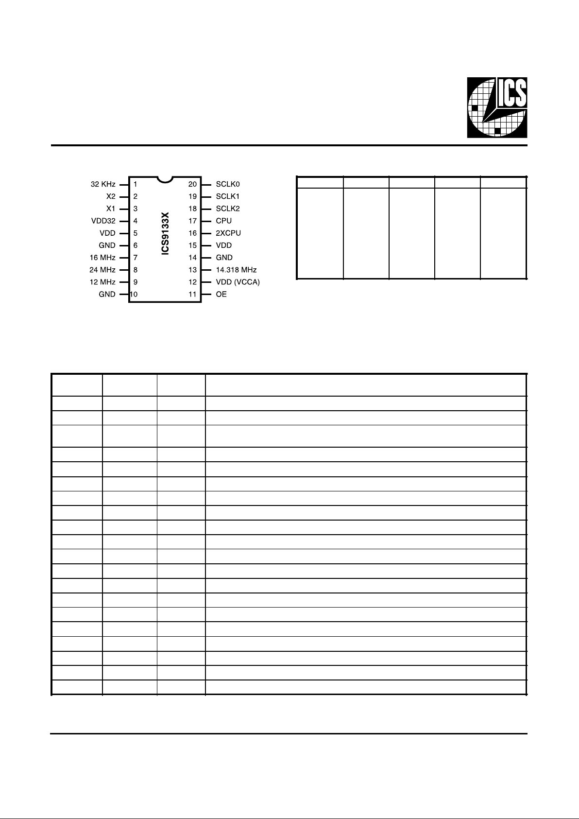
Pin Configuration Decoding Tabl e for CPU Clock
Pin Descriptions
* Only at 5V supply voltage
20-Pin PDIP or SOIC
PIN
NUMBER
PIN NAME TYPE DESCRIPTION
1 32 kHz Output 32.768 kHz buffered output, powered by VDD32.
2 X2 Output Connect 32.768 kHz crystal. Includes internal XTAL load capacitance.
3 X1 Input
Connect 32.768 kHz crystal. This pin includes internal XTAL load capacitance and
feedback bias for a 32.768 kHz crystal.
4 VDD32 - Power supply for 32 kHz oscillator only.
5 VDD - Power supply (+3.3 to +5.0V).
6 GND - GROUND.
7 16 MHz Output 16 MHz clock output.
8 24 MHz Output 24 MHz clock output.
9 12 MHz Output 12 MHz clock output.
10 GND - GROUND.
11 OE Input OE tristate outputs when low. Has internal pull-up.
12 VDD - Power supply (+3.3 to +5.0V).
13 14.318 MHz Output 14.318 MHz clock output.
14 GND - GROUND.
15 VDD - Power supply (+3.3 to +5.0V).
16 2XCPU Output 2XCPU clock output (see decoding table).
17 CPU Output CPU clock output (see decoding table).
18 SCLK2 Input CPU clock frequency SELECT2. Has internal pull-up.
19 SCLK1 Input CPU clock frequency SELECT1. Has internal pull-up.
20 SCLK0 Input CPU clock frequency SELECT0. Has internal pull-up.
SCLK22 SCLK21 SCLK20 2XCPU CPU
0
0
0
0
1
1
1
1
0
0
1
1
0
0
1
1
0
1
0
1
0
1
0
1
8
16
32
40
50
66.6
80*
100*
4
8
16
20
25
33.3
40*
50*
Page 3
3
ICS9133X
Block Diagram for ICS9133X
Recommended External Circuit
Reference
Clock
32.768 kHz
crystal
32.768 kHz
14.318 MHz
14.318 MHz
Clock
Generator
Output
Buffers
CPU
OE
16 MHz
12 MHz
24 MHz
CPU Clock
2XCPU
Peripheral
Clocks
Output
Buffers
Output
Buffers
Frequency Select
3
/
Notes:
1. The external components shown should be placed as close to the device as possible.
2. Pins 5 and 15 should be connected together externally. One decoupling capacitor may suffice for both pins.
3. May be part of system decoupling.
4. Crystal load capacitance and feedback bias contained internally on the X1, X2 pins.
20
19
18
17
16
15
14
13
12
11
1
2
3
4
5
6
7
8
9
10
0.1µF
0.1µF
0.1µF
2.2µF
0.1µF
(Note 3)
32.768
kHz
VDDX
(Note 4)
VDD
IC S 91 33 X
Page 4

4
ICS9133X
Electrical Characteristics at 3.3V
Operating VDD = +3.0V to 3.7V; TA =0°C to 70°C unless otherwise stated
Note: 1. Parameter is guaranteed by design and characterization. Not 100% tested in production.
2. 32 kHz output duty cycle is dependent on crystal used.
Absolute Maximum Ratings
VDD referenced to GND....................................................................................................................................................... 7V
Operating temperature under bias ....................................................................................................................... 0°C to +70°C
Storage temperature.........................................................................................................................................-40°C to +150°C
Voltage on I/O pins referenced to GND........................................................................................GND -0.5V to VDD +0.5V
Power dissipation..........................................................................................................................................................0.5 Watts
Stresses above those listed under Absolute Maximum Ratings may cause permanent damage to the de vice. T his is a stress rating
only and functional operation of the device at these or any other conditions above those indicated in the operational sections of
the specifications is not implied. Exposure to absolute maximum rating conditions for extended periods may affect product
reliability.
DC Charact eristi cs
PARAMETER SYMBOL TEST CONDITIONS MIN TYP MAX UNITS
Input Low Voltage V
IL
- - 0.2V
DD
V
Input High Voltage V
IH
0.7V
DD
--V
Input Low Current I
IL
VIN=0V (Pull-up) -12 - - µA
Input High Current I
IH
VIN=V
DD
-2-2µA
Output Low Voltage
1
V
OL
IOL=4mA - - 0.1 V
Output High Voltage
1
V
OH
IOH=-1mA VDD-.1V - - V
Output High Current
1
V
OH
IOH=-4mA - - - V
Output High Current
1
V
OH
IOH=-8mA 2.4 - - V
Output Frequency Change
over Supply and
Temperature
1
F
D
With respect to typical
frequency
1
- .005 0.05 %
Short Circuit Current
1
I
SC
Each output clock - 15 - mA
Supply Current I
DD
No load, 40 MHz - 10 - mA
V
DD
32 Supply Current I
DD
32 No load, VDD32=3.7V - 5 12 µA
V
DD
32 Supply Voltage V
DD
32 VDD=0 to 3.7V, 32 kHz output
operating
2.0- -V
Pull-up Resistor Value Rpu - 620 - k½
AC Charact eristi cs
Input Clock Rise Time
1
t
ICr
--5µs
Input Clock Fall Time
1
t
ICf
--5µs
Output Rise Time
1
t
r
15pF load, 0.8 to 2.0V - 1.5 2 ns
Rise Time
1
t
f
15pF load, 20% to 80% V
DD
- 2.54ns
Output Fall Time
1
t
f
15pF load, 2.0 to 0.8V - 1.5 2 ns
Fall Time
1
t
f
15pF load, 80% to 20% V
DD
- 2.54ns
Duty Cycle
1
d
t
15pF load @ Vth=1.4V 43/57 48/52 57/43 %
Duty Cycle, reference
clocks
1
d
t
15pF load @ 1.4V
2
40/60 43/57 60/40 %
Jitter, One Sigma
1
As compared with clock period. - 1 3 %
Jitter, Absolute
1
t
jab
-25%
Input Frequency
1
f
i
25 32.768 40 kHz
Clock Skew between any
Clock #2 outputs
1
T
sk
- 100 500 ps
Power-up Time
1
t
pu
From off to 40 MHz - 1,000 - ms
Page 5

5
ICS9133X
Electrical Characteristics at 5V
VDD = +5.0V ±10%; TA =0°C to 70°C unless otherwise stated
Note: 1. Parameter is guaranteed by design and characterization. Not 100% tested in production.
2. 32 kHz output duty cycle is dependent on crystal used.
DC Charact eristics
PARAMETER SYMBOL TEST CONDITIONS MIN TYP MAX UNITS
Input Low Voltage V
IL
--0.2VDDV
Input High Voltage V
IH
0.7V
DD
--V
Input Low Current I
IL
VIN=0V (Pull-up) -15 - - µA
Input High Current I
IH
VIN=V
DD
-2 - 2 µA
Output Low Voltage
1
V
OL
IOL=4mA - - 0.1 V
Output High Voltage
1
V
OH
IOH=-1mA VDD-.1V - - V
Output High Voltage
1
V
OH
IOH=-4mA - - - V
Output High Voltage
1
V
OH
IOH=-8mA 2.4 - - V
Output Frequency Change
over Supply and
Temperature
1
F
D
With respect to typical
frequency
1
- .005 0.05 %
Short Circuit Current
1
I
SC
Each output clock - 33 - mA
Supply Current I
DD
No load, 40 MHz - 17 - mA
V
DD
32 Supply Current IDD 32 No load, VDD32=5.5V - 7.5 20 µA
V
DD
32 Supply Voltage V
DD
32
V
DD
=0 to 5.5V, 32 kHz output
operating
2.0- -V
Pull-up Resistor Value R
pu
-380-k½
AC Charact eristics
Input Clock Rise Time
1
t
ICr
--5µs
Input Clock Fall Time
1
t
ICf
--5µs
Output Rise Time
1
t
r
15pF load, 0.8 to 2.0V - 1 1.5 ns
Rise Time
1
t
r
15pF load, 20% to 80% V
DD
-23ns
Output Fall Time
1
t
f
15pF load, 2.0 to 0.8V - 1 1.5 ns
Fall Time
1
t
f
15pF load, 80% to 20% V
DD
-23ns
Duty Cycle
1
d
t
15pF load @ Vth=1.4V 43/57 48/52 57/43 %
Duty Cycle, reference
clocks
1
d
t
15pF load @ 1.4V
2
40/60 43/57 60/40 %
Jitter, One Sigma
1
t
j1s
As compared with clock period.
-13%
Jitter, Absolute
1
t
jab
-25%
Input Frequency
1
f
i
25 32.768 40 kHz
Clock Skew between any
Clock #2 outputs
1
T
sk
- 100 500 ps
Power-up Time
1
t
pu
From off to 40 MHz - 10 - ms
Page 6

6
ICS9133X
Typical 32 kHz Suppl y Current
14
12
10
µA
8
6
4
2
0
0123
Vdd
456
C
L
= 25pF
C
L
= 15pF
C
L
= 0pF
Page 7

7
ICS9133X
20-Pin DIP Package
Ordering Information
Package Information
1.025
0.260
0.325
0.010
0.360
0 ~ 5°
0.130
0.015
min
0.060
0.018
0.100
0.130
Example:
ICS XXXX-PPP M X#W
Lead Count & Package Width
Lead Count=1,2, or 3 digits
W=0.3" SOIC or 0.6" DIP; None=Standard Width
Package Type
N=DIP (Plastic)
Device Type (consists of 3 or 4-digit numbers)
Prefix
ICS, AV=Standard Device
Pattern Number (2 or 3-digit number for parts with ROM code patterns)
Page 8

8
ICS9133X
5 Deg. Typ.
LEAD COUNT
DIMENSION L
20L
.504
0.101 ± 0.010
0.328 ± 0.010
0.015 x 45 Deg.
0.406 ± 0.010
0.020
0.092 ± 0.005
0.041 ± 0.003
0.296 ± 0.005
0.010
0.050
Pitch Typ.
0.008 ± 0.006
5 Deg. Typ. ± 5
5 Deg. Typ.
L ± .008
0.029
Typ.
0.018
0.047R
Pin 1
SOIC Packages (Widebody)
Ordering Information
ICS9133X-01CW20
Example:
ICS XXXX-PPP M X#W
Lead Count & Package Width
Lead Count=1,2, or 3 digits
W=0.3" SOIC or 0.6" DIP; None=Standard Width
Package Type
W=DIP (Plastic)
Device Type (consists of 3 or 4-digit numbers)
Prefix
ICS, AV=Standard Device
Pattern Number (2 or 3-digit number for parts with ROM code patterns)
ICS reserves the right to make changes in the device data identified in this publication
without further notice. ICS advises its customers to obtain the latest version of all device
data to verify that any information being relied upon by the customer is current and accurate.
 Loading...