

Page 1
Integrated
Circuit
Systems, Inc.
FeaturesGeneral Description
ICS9120-52
Frequency Generator for CD-ROM Systems
9120-52 Rev B 052497P
Block Diagram
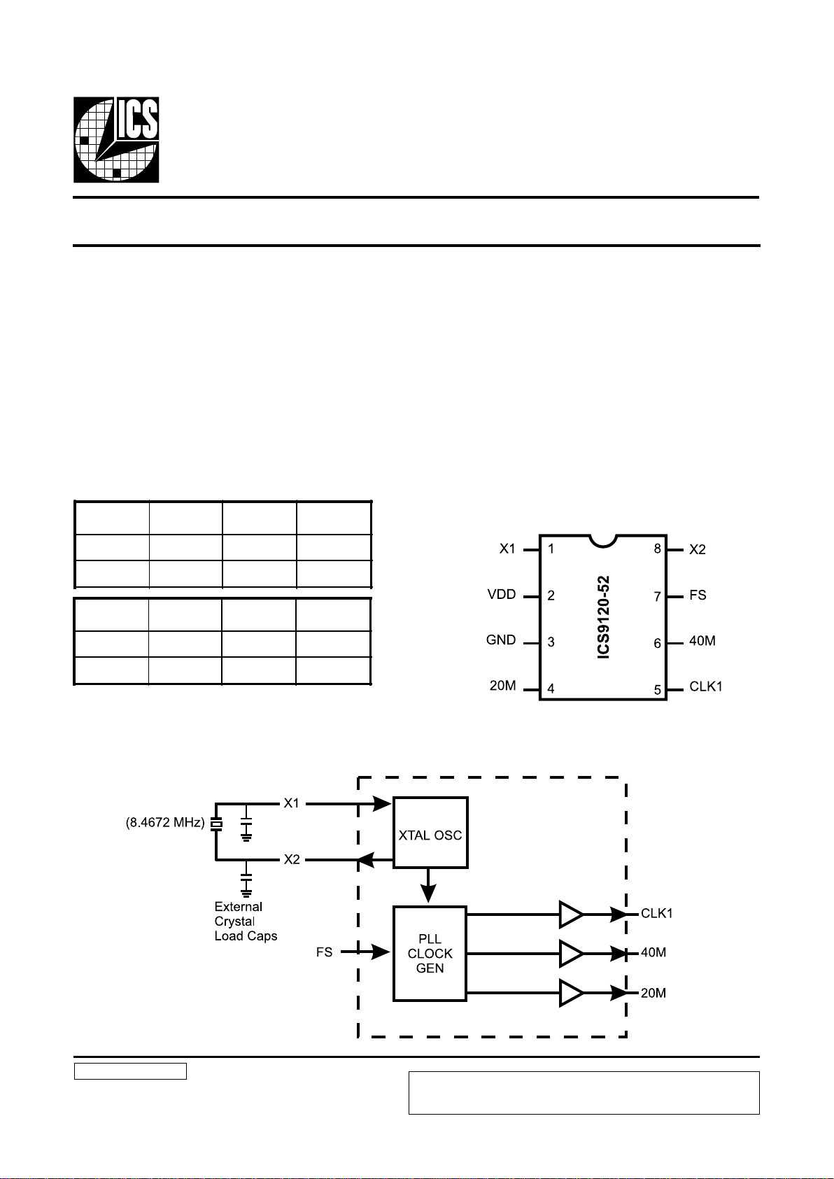
• Generates 33.8688 MHz or 42.83 MHz decode clocks
plus the 20 and 40 MHz fixed clocks
• Single 8.4672 MHz crystal or system clock reference
• 200ps one sigma jitter maintains 16-bit performance
• Output rise/fall times less than 2.0ns
• On-chip loop filter components
• 3.3V -5V supply range
• 8-pin, 150-mil SOIC
Applications
• Specifically designed to support the high performance
requirements of CD-ROM drive systems
The ICS9120-52 is a high performance frequency generator
designed to support digital compact disk drive systems. It
offers all clock frequencies required for the servo and
decoder sections of these devices. These frequencies are
synthesized from a single 16.9344 MHz on-chip oscillator.
High accuracy, low jitter PLLs meet the 150 ppm frequency
tolerance required by these systems. Fast output clock
edge rates minimize board induced jitter.
Unlike competitive devices, the ICS9120-52 operates over
the entire 3.0-5.5V range.
ICS reserves the right to make changes in the device data identified in this publication
without further notice. ICS advises its customers to obtain the latest version of all
device data to verify that any information being relied upon by the customer is current
and accurate.
Pin Configuration
8-Pin SOIC
Functionality
X1, X2
(MHz)
FS Divisor CLK 1
8.4672 0 X12÷3 33.8688
86.4672 1 X61÷6 42.83
Clock
X1, X2
(MHz)
Divisor
Output
(MHz)
20M 8.4672 X 52÷11÷2 20.0134
40M 8.4672 X52÷11 40.0268
Page 2
2
ICS9120-52
Pin Descriptions
PIN
NUMBER
PIN
NAME
TYPE DESCRIPTION
1 X1 Input Crystal or external clock source. Has feedback bias for crystal.
2 VDD Power +Power supply input.
3 GND Power Ground return for Pin 2.
4 20M Output 20 MHz fixed output clock.
5 CLK1 Output 33.8/42.83 MHz selectable clock output.
6 40M Output 40 MHz fixedoutput clock.
7 FS Input Input selector for CLK1.
8 X2 Output Crystal output drive.
Page 3

3
ICS9120-52
Absolute Maximum Ratings
Electrical Characteristics at 5 V
VDD = +4.5 to +5.5 V , TA = 0 to 70oC unless otherwise stated
*Parameter is guaranteed by design and characterization. Not 100% tested in production.
A VDD, VDD referenced to GND ...........................................................................7V
Operating temperature under bias...................................................... 0oC to +70oC
Storage temperature ....................................................................... -65oC to +150oC
Voltage on I/O pins referenced to GND ......................... GND -0.5V to VDD +0.5V
Power dissipation ...................................................................................... 0.5 Watts
Stresses above those listed under Absolute Maximum Ratings may cause permanent damage to the device. This is a stress
rating only and functional operation of the device at these or any other conditions above those indicated in the operational
sections of the specifications is not implied. Exposure to absolute maximum rating conditions for extended periods may affect
product reliability.
DC Characteristics
PAR AMETER SYMBOL TEST CONDITIONS MIN TYP MAX UNITS
Input Low Voltage V
IL
--0.8V
Input High Voltage V
IH
2.0 - - V
Input Low Current I
IL
VIN=0V -18.0 -8.3 - µ A
Input High Current I
IH
VIN=V
DD
--5.0µA
Output Low Voltage V
OL
*I
OL
=+10mA - 0.15 0.4 V
Output High Voltage VOH*I
OH
=-30mA 2.4 3.7 - V
Output Low Current I
OL
*V
OL
=0.8V 25.0 45.0 - mA
Output High Current IOH*V
OH
=2.4V - -53.0 -35.0 mA
Supply Current I
DD
Unloaded - 26.0 50.0 mA
Pull-up Resistor Value R
PU
* - 400.0 800.0 k ohm
AC Characteristics
Rise Time T
r
* 15pF load, 0.8 to 2.0V - 0.9 2.0 ns
Fall Tim e T
f
* 15pF load, 2.0 to 0.8V - 0.7 1.5 ns
Rise Time Tr* 15pF load, 20% to 80% - 1.8 3.25 ns
Fall Tim e T
f
* 15pF load, 80% to 20% - 1.4 2.5 ns
Duty Cycle D
t
*
15pF load @
50% of V
DD
45.0 50.0 55.0 %
Jitter, On e Sigm a T
j1s
* For all frequencies - 100.0 200.0 ps
Jitter, Ab solute T
jab
* For all frequencies -500.0 300.0 500.0 ps
Input Frequency Range F
i
* 8.0 8.4 100.0 MHz
Output Frequency Range Fo* 11.0 - 42.0 MHz
Output Mean Frequency
Accuracy vs. Target
F
oa
* With 8.4672 MHz input -0.125 - -0.04 %
Power-up Time Tpu* 0 to 33.8 MHz - 5.5 12.0 ms
Crystal Input Capacitance C
inx
* X1 (Pin 1), X2 (Pin 8) -5 - -
pF
Page 4

4
ICS9120-52
Electrical Characteristics at 3.3 V
VDD = +3.0 to +3.7 V, TA = 0OC-70oC unless otherwise stated
*Parameter is guaranteed by design and characterization. Not 100% tested in production.
DC Characteristics
PARAM ETER SYMBOL TEST CONDITIONS MIN TYP MAX UNITS
Input Low Voltage V
IL
- - 0.2V
DD
V
Input High Voltage V
IH
0.7V
DD
- - V
Input Low Current I
IL
VIN=0V -8.0 -3.6 - µA
Input High Current I
IH
VIN=V
DD
--5.0µA
Output Low Voltage V
OL
*IOL=6.0mA - 0.05V
DD
0.1 V
Output High Voltage V
OH
*IOH=4.0mA 0.85V
DD
0.94V
DD
-V
Output Low Current I
OL
*V
OL
=0.2V
DD
15.0 24.0 - mA
Output High Current I
OH
*V
OH
=0.7V
DD
- -13.0 -8.0 mA
Supply Current I
DD
Unloaded - 17.0 40.0 mA
Pull-up Resistor Value R
PU
* - 620.0 900.0 k ohm
AC Characteristics
Rise Time Tr* 15pF load 0.8 to 2.0V - 1.5 4.0 ns
Fall Time T
f
* 15pF load 2.0 to 0.8V - 1.0 3.0 ns
Rise Time T
r
* 15pF load 20% to 80% - 2.2 4.0 ns
Fall Time T
f
* 15pF load 80% to 20% - 1.5 3.0 ns
Duty Cycle D
t
*
15pF load @ 50% of
V
DD
; Except R EFCLK
45.0 50.0 55.0 %
Jitter, One Sigm a T
j1s
*
For all frequen cies
except REFCLK
- 150.0 200 ps
Jitter Absolu te T
jab
*
For all frequen cies
except REFCLK
-550.0 330.0 550.0 ps
Input Frequency Range F
i
* 8.0 8.4 10.0 MHz
Output Frequency Range F
o
* 11.0 - 38.0 MHz
Output Mean Frequency
Accuracy vs. Target
F
oa
* With 8.4672 MHz input -0.125 - -0.04 %
Power-up Time T
pu
*
0 to 33.8 MHz - 5.5 12.0 ms
Crystal Input Capacitance C
inx
*
X1 (Pin 1),
X2 (Pin 8)
-5-pF
Page 5

5
ICS9120-52
Ordering Information
ICS9120M-52
0.194
0.031
0.024
0.016
0.050
0.006
± 0.004
0.238
0.154
0.015
0.063
0.025
0.008
8-Pin SOIC Package
Example:
ICS XXXX M-PPP
Package Type
M =SOIC
Device Type (consists of 3 or 4-digit numbers)
Prefix
ICS, AV=Standard Device
Pattern Number (2 or 3-digit number for parts with ROM code pattern)
ICS reserves the right to make changes in the device data identified in this publication
without further notice. ICS advises its customers to obtain the latest version of all
device data to verify that any information being relied upon by the customer is current
and accurate.
 Loading...