

Page 1

Integrated
Circuit
Systems, Inc.
ICS8344-01
LOW SKEW, 1-TO-24
DIFFERENTIAL-TO-L VCMOS FANOUT BUFFER
GENERAL DESCRIPTION
,&6
HiPerClockS™
can accept most standard differential input levels. The
ICS8344-01 is designed to translate any differential signal
levels to L VCMOS levels. The low impedance LVCMOS outputs are designed to drive 50Ω series or parallel terminated
transmission lines. The effective fanout can be increased to
48 by utilizing the ability of the outputs to drive two series
terminated lines. Redundant clock applications can make use
of the dual clock input. The dual clock inputs also facilitate
board level testing. The clock enable is internally synchronized to eliminate runt pulses on the outputs during asynchronous assertion/deassertion of the clock enable pin. The
outputs are driven low when disabled. The ICS8344-01 is
characterized at full 3.3V , full 2.5V and mixed 3.3V input and
2.5V output operating supply modes.
Guaranteed output and part-to-part skew characteristics
make the ICS8344-01 ideal for those clock distribution
applications demanding well defined performance and
repeatability.
The ICS8344-01 is a low voltage, low skew
fanout buffer and a member of the HiPerClockS™
family of High Performance Clock Solutions from
ICS. The ICS8344-01 has two selectable clock
inputs. The CLK0, nCLK0 and CLK1, nCLK1 pairs
FEATURES
• 24 L VCMOS outputs, 7Ω typical output impedance
• 2 selectable CLKx, nCLKx inputs
• CLK0, nCLK0 and CLK1, nCLK1 pairs can accept the
following input levels: L VDS, LVPECL, L VHSTL, SSTL,
HCSL
• Output frequency up to 250MHz
• Translates any single ended input signal to LVCMOS with
resistor bias on nCLK input
• Synchronous clock enable
• Output skew: 200 ps (maximum)
• Part-to-part skew: 900ps (maximum)
• Bank skew: 85ps (maximum)
• Propagation delay: 5ns (maximum)
• 3.3V , 2.5V or mixed 3.3V , 2.5V operating supply modes
• 0°C to 70°C ambient operating temperature
• Industrial temperature information available upon request
BLOCK DIAGRAM PIN ASSIGNMENT
GND
V
Q14
CLK_SEL
CLK0
nCLK0
CLK1
nCLK1
CLK_EN
OE
1
0
Q0 - Q7
Q8 - Q15
Q16 - Q23
LE
Q
nD
Q16
Q17
V
DDO
GND
Q18
Q19
Q20
Q21
V
DDO
GND
Q22
Q23
Q15
DDO
48 47 46 45 44 43 42 41 40 39 38 37
1
2
3
4
5
6
7
8
9
10
11
12
ICS8344-01
13 14 15 16 17 18 19 20 21 22 23 24
nCLK1
VDDGND
CLK_SEL
48-Lead LQFP
7mm x 7mm x 1.4mm
Y Package
Top View
Q13
CLK1
Q12
Q11
VDDGND
GND
Q10
CLK0
nCLK0
V
DDO
Q8
Q9
nc
OE
CLK_EN
36
35
34
33
32
31
30
29
28
27
26
25
Q7
Q6
V
DDO
GND
Q5
Q4
Q3
Q2
V
DDO
GND
Q1
Q0
8344AY-01 www.icst.com/products/hiperclocks.html REV. B AUGUST 6, 2001
1
Page 2
Integrated
Circuit
Systems, Inc.
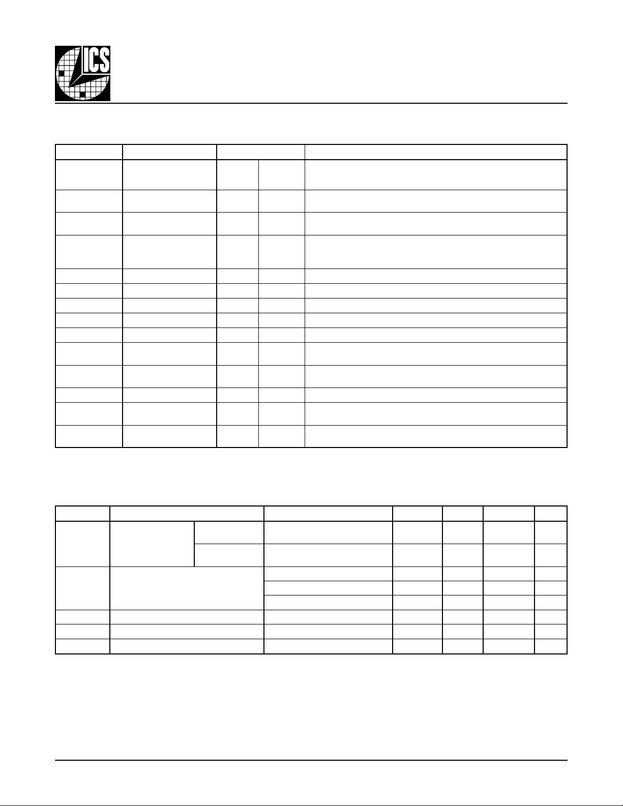
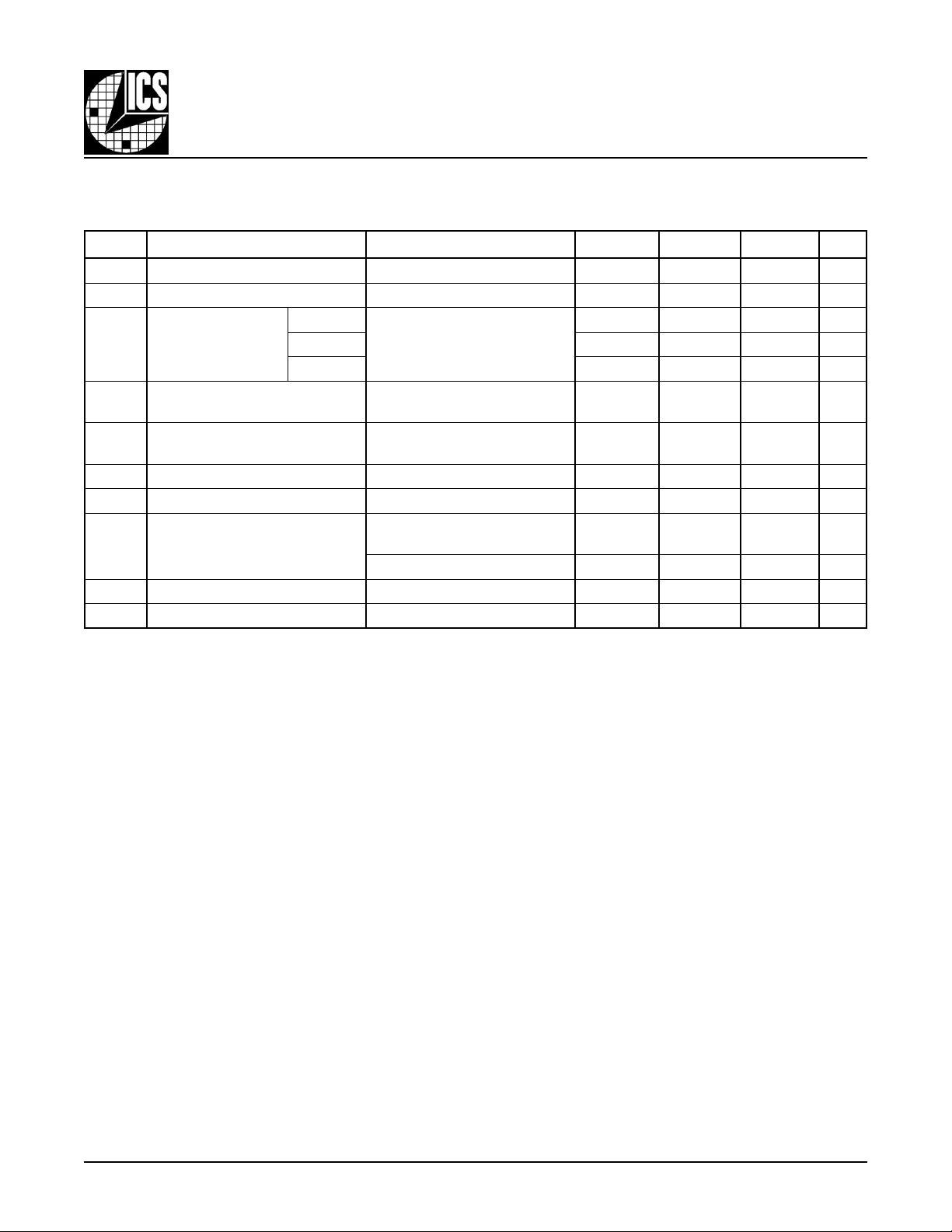
TABLE 1. PIN DESCRIPTIONS
rebmuNemaNepyTnoitpircseD
6,5,2,1
21,11,8,7
,82,9,3
54,93,43
,81,41,01,4
64,04,33,72
31LES_KLCtupnInwodlluP
91,51V
611KLCntupnIpulluP.tupnikcolcLCEPVLlaitnereffidgnitrevnI
711KLCtupnInwodlluP.tupnikcolcLCEPVLlaitnereffidgnitrevni-noN
020KLCntupnIpulluP.tupnikcolcLCEPVLlaitnereffidgnitrevnI
120KLCtupnInwodlluP.tupnikcolcLCEPVLlaitnereffidgnitrevni-noN
22NE_KLCtupnIpulluP
32EOtupnIpulluP
42cndesunU.tcennocoN
03,92,62,52
63,53,23,13
24,14,83,73
84,74,44,34
pulluP
:ETON
dna
91Q,81Q,71Q,61Q
32Q,22Q,12Q,02Q
V
ODD
DNGrewoP.dnuorgottcennoC.dnuorgylppusrewoP
DD
3Q,2Q,1Q,0Q
7Q,6Q,5Q,4Q
11Q,01Q,9Q,8Q
51Q,41Q,31Q,21Q
tuptuO7.stuptuo32Qurht61Q Ω .ecnadepmituptuolacipyt
rewoP.V5.2roV3.3tcennoC.snipylppustuptuO
rewoP.V5.2roV3.3tcennoC.snipylppusevitisoP
tuptuO7.stuptuo7Qurht0Q Ω .ecnadepmituptuolacipyt
tuptuO7.stuptuo51Qurht8Q Ω .ecnadepmituptuolacipyt
nwodlluP
ICS8344-01
LOW SKEW, 1-TO-24
DIFFERENTIAL-TO-L VCMOS FANOUT BUFFER
,stupniKLCn,1KLCstceles,HGIHnehW.tupnitceleskcolC
.stupni0KLCn,0KLCstceles,WOLnehW
.sslevelecafretniLTTVL/SOMCVL
.stuptuokcolcgnilbasiddnagnilbaneroflortnocgnizinorhcnyS
.slevelecafretniSOMCVL
stuptuofognilbasiddnagnilbaneslortnoC.elbanetuptuO
.32Qurht0Q
.seulavlacipytrof,scitsiretcarahCniP,2elbaTeeS.srotsisertupnilanretniotsrefer
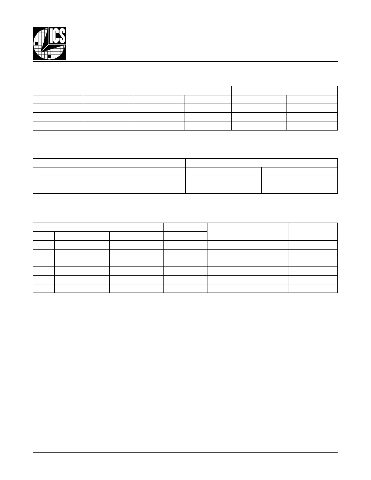
TABLE 2. PIN CHARACTERISTICS
lobmySretemaraPsnoitidnoCtseTmuminiMlacipyTmumixaMstinU
,0KLCn,0KLC
C
NI
C
DP
R
PULLUP
R
R
8344AY-01 www.icst.com/products/hiperclocks.html REV. B AUGUST 6, 2001
NWODLLUP
TUO
ecnaticapaCtupnI
)tuptuorep(
rotsiseRpulluPtupnI 15KΩ
rotsiseRnwodlluPtupnI 15KΩ
ecnadepmItuptuO 7
1KLCn,1KLC
,LES-KLC
EO,NE_KLC
ecnaticapaCnoitapissiDrewoP
2
4Fp
4Fp
Fp
Fp
Fp
Ω
Page 3
Integrated
Circuit
Systems, Inc.
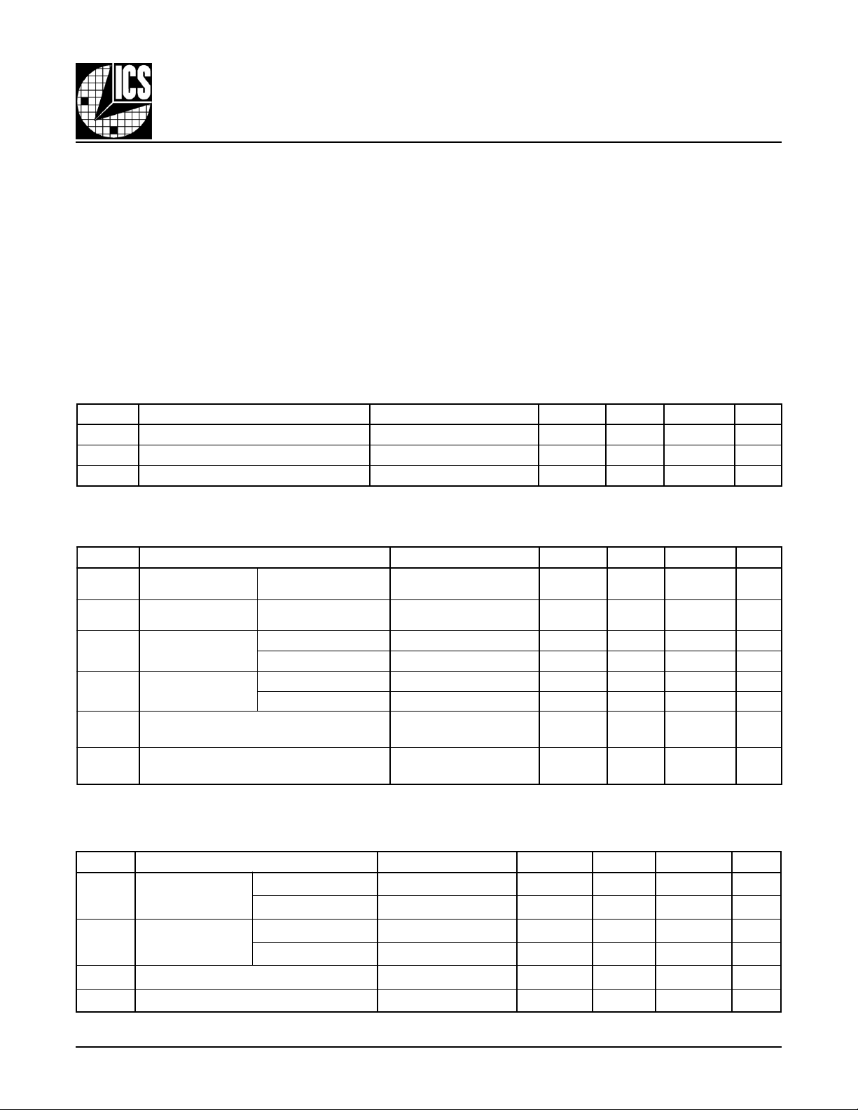
TABLE 3A. OUPUT ENABLE FUNCTION TABLE
1knaB2knaB3knaB
tupnItuptuOtupnItuptuOtupnItuptuO
EO7Q-0QEO51Q-8QEO32Q-61Q
0Z-iH0Z-iH0 Z-iH
1delbanE1delbanE1 delbanE
TABLE 3B. CLOCK SELECT FUNCTION TABLE
tupnIlortnoCkcolC
LES_KLC0KLCn,0KLC1KLCn,1KLC
0detceleSdetceles-eD
1detceles-eDdetceleS
ICS8344-01
LOW SKEW, 1-TO-24
DIFFERENTIAL-TO-L VCMOS FANOUT BUFFER
TABLE 3C. CLOCK INPUT FUNCTION TABLE
stupnIstuptuO
EO1KLC,0KLC1KLCn,0KLCn32Qurht0Q
10 1 WOLdednEelgniSotlaitnereffiDgnitrevnInoN
11 0 HGIHdednEelgniSotlaitnereffiDgnitrevnInoN
10 1ETON;desaiBWOLlaitnereffiDotdednEelgniSgnitrevnInoN
11 1ETON;desaiBHGIHlaitnereffiDotdednEelgniSgnitrevnInoN
11ETON;desaiB0HGIHlaitnereffiDotdednEelgniSgnitrevnI
11ETON;desaiB1WOLlaitnereffiDotdednEelgniSgnitrevnI
.sleveldedneelgnistpeccaottupni
edoMtuptuOottupnIytiraloP
laitnereffidehtgniriwsessucsidhcihw,8erugiF,11egapnonoitcesnoitamrofnInoitacilppAehtotreferesaelP:1ETON
8344AY-01 www.icst.com/products/hiperclocks.html REV. B AUGUST 6, 2001
3
Page 4
Integrated
Circuit
Systems, Inc.
ICS8344-01
LOW SKEW, 1-TO-24
DIFFERENTIAL-TO-L VCMOS FANOUT BUFFER
Supply Voltage, V
Inputs, V
Outputs, V
DDx
I
O
Package Thermal Impedance, θ
Storage T emperature, T
STG
JA
4.6V
-0.5V to VDD + 0.5V
-0.5V to V
DDO
+ 0.5V
47.9°C/W (0lfpm)
-65°C to 150°C
Stresses beyond those listed under Absolute Maximum Ratings may cause permanent damage to the device. These ratings
are stress specifications only. Functional operation of product at these conditions or any conditions beyond those listed in
DC Characteristics
the
or
AC Characteristics
is not implied. Exposure to absolute maximum rating conditions for extended
periods may affect product reliability .
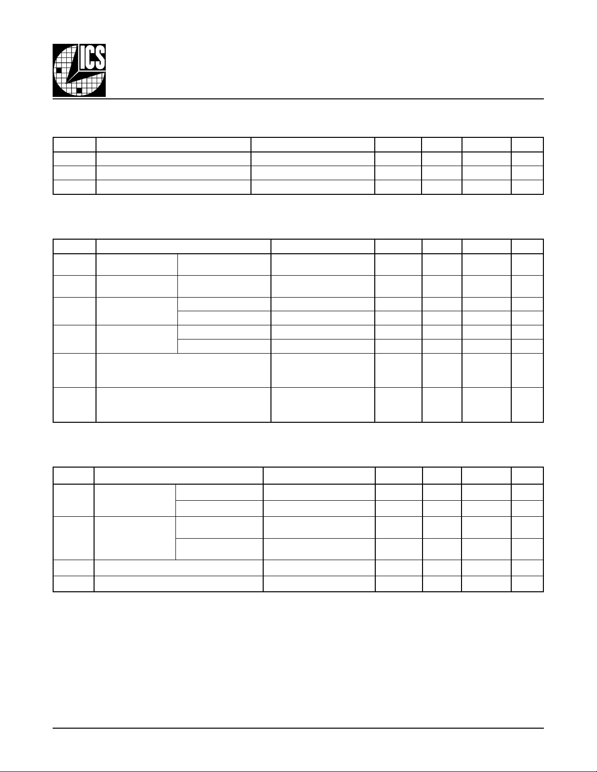
TABLE 4A. POWER SUPPLY DC CHARACTERISTICS, V
DD
= V
= 3.3V±5%, TA = 0°C TO 70°C
DDO
lobmySretemaraPsnoitidnoCtseTmuminiMlacipyTmumixaMstinU
V
DD
V
ODD
I
DD
TABLE 4B. LVCMOS DC CHARACTERISTICS, V
egatloVylppuSevitisoP 531.33.3564.3V
egatloVylppuStuptuO 531.33.3564.3V
tnerruCylppuSrewoPtnecseiuQ 59Am
= V
DD
= 3.3V±5%, TA = 0°C TO 70°C
DDO
lobmySretemaraPsnoitidnoCtseTmuminiMlacipyTmumixaMstinU
V
HI
V
LI
I
HI
I
LI
V
HO
V
LO
egatloVhgiHtupnI
EO
egatloVwoLtupnI
EO
tnerruChgiHtupnI
tnerruCwoLtupnI
EO,NE_KLCV
LES_KLCV
EO,NE_KLCV
LES_KLCV
egatloVhgiHtuptuO
egatloVwoLtuptuO
,NE_KLC,LES_KLC
,NE_KLC,LES_KLC
V=
DD
NI
V=
DD
NI
DD
DD
V
V=
DD
ODD
I
HO
V
V=
DD
ODD
I
LO
V564.3=5Aµ
V564.3=051Aµ
V,564.3=
V0=051-Aµ
NI
V,564.3=
V0=5-Aµ
NI
V531.3=
Am63-=
V531.3=
Am63=
28.3V
3.0-8.0V
7.2V
5.0V
TABLE 4C. DIFFERENTIAL DC CHARACTERISTICS, V
DD
= V
= 3.3V±5%, TA = 0°C TO 70°C
DDO
lobmySretemaraPsnoitidnoCtseTmuminiMlacipyTmumixaMstinU
I
HI
tnerruChgiHtupnI
1KLC,0KLCV
1KLCn,0KLCnV
1KLCn,0KLCnV
I
LI
V
PP
V
RMC
8344AY-01 www.icst.com/products/hiperclocks.html REV. B AUGUST 6, 2001
tnerruCwoLtupnI
1KLC,0KLCV
egatloVtupnIkaePot-kaeP 3.03.1V
2,1ETON:egatloVtupnIedoMnommoC 9.02V
VsadenifedsiegatlovedomnommoC:2ETON
.
V=
DD
NI
V=
DD
NI
DD
DD
4
V564.3=5Aµ
V564.3=051Aµ
V,V564.3=
V0=051-Aµ
NI
V,V564.3=
V0=5-Aµ
NI
Vsi1KLCn,1KLCdna0KLCn,0KLCrofegatlovtupnimumixameht,snoitacilppadedneelgnisroF:1ETON
DD
.V3.0+
Page 5
Integrated
Circuit
Systems, Inc.
ICS8344-01
LOW SKEW, 1-TO-24
DIFFERENTIAL-TO-L VCMOS FANOUT BUFFER
TABLE 4D. POWER SUPPLY DC CHARACTERISTICS, V
DD
lobmySretemaraPsnoitidnoCtseTmuminiMlacipyTmumixaMstinU
V
DD
V
ODD
I
DD
egatloVylppuSevitisoP 531.33.3564.3V
egatloVylppuStuptuO 573.25.2526.2V
tnerruCylppuSrewoPtnecseiuQ 59Am
TABLE 4E. L VCMOS DC CHARACTERISTICS, VDDI = V
lobmySretemaraPsnoitidnoCtseTmuminiMlacipyTmumixaMstinU
V
HI
V
LI
I
HI
I
LI
V
HO
V
LO
egatloVhgiHtupnI
EO
egatloVwoLtupnI
EO
tnerruChgiHtupnI
tnerruCwoLtupnI
EO,NE_KLCV
LES_KLCV
EO,NE_KLCV
LES_KLCV
egatloVhgiHtuptuO
egatloVwoLtuptuO
= 3.3V±5%, V
= 3.3V±5%, V
DD
,NE_KLC,LES_KLC
,NE_KLC,LES_KLC
DD
DD
DD
DD
V
V
I
HO
V
V
I
= 2.5V±5%, TA = 0°C TO 70°C
DDO
= 2.5V±5%, TA = 0°C TO 70°C
DDO
V=
NI
V=
NI
DD
ODD
DD
ODD
LO
V564.3=5Aµ
V564.3=051Aµ
V,564.3=
V0=051-Aµ
NI
V,564.3=
V0=5-Aµ
NI
V531.3=
V573.2=
Am72-=
V531.3=
V573.2=
Am72=
28.3V
3.0-8.0V
9.1V
4.0V
TABLE 4F. DIFFERENTIAL DC CHARACTERISTICS, V
= 3.3V±5%, V
DD
= 2.5V±5%, TA = 0°C TO 70°C
DDO
lobmySretemaraPsnoitidnoCtseTmuminiMlacipyTmumixaMstinU
I
HI
tnerruChgiHtupnI
1KLC,0KLCV
1KLCn,0KLCn
1KLCn,0KLCnV
I
LI
tnerruCwoLtupnI
1KLC,0KLC
V
PP
V
RMC
8344AY-01 www.icst.com/products/hiperclocks.html REV. B AUGUST 6, 2001
egatloVtupnIkaeP-ot-kaeP 3.03.1V
2,1ETON;egatloVtupnIedoMnommoC 9.02V
.
VsadenifedsiegatlovedomnommoC:2ETON
V=
DD
NI
V=
DD
NI
V
DD
V
NI
V
DD
V
NI
V564.3=5Aµ
V564.3=051Aµ
,V564.3=
V0=
,V564.3=
V0=
051-Aµ
5-Aµ
Vsi1KLCn,1KLCdna0KLCn,0KLCrofegatlovtupnimumixameht,snoitacilppadedneelgnisroF:1ETON
.V3.0
+DD
5
Page 6

Integrated
Circuit
Systems, Inc.
ICS8344-01
LOW SKEW, 1-TO-24
DIFFERENTIAL-TO-L VCMOS FANOUT BUFFER
TABLE 4G. POWER SUPPLY DC CHARACTERISTICS, V
lobmySretemaraPsnoitidnoCtseTmuminiMlacipyTmumixaMstinU
V
DD
V
ODD
I
DD
TABLE 4H. LVCMOS DC CHARACTERISTICS, V
lobmySretemaraPsnoitidnoCtseTmuminiMlacipyTmumixaMstinU
V
HI
V
LI
I
HI
I
LI
V
HO
V
LO
egatloVylppuSevitisoP 573.25.2526.2V
egatloVylppuStuptuO 573.25.2526.2V
tnerruCylppuSrewoPtnecseiuQ 59Am
= V
DD
egatloVhgiHtupnI
EO
egatloVwoLtupnI
EO
tnerruChgiHtupnI
tnerruCwoLtupnI
EO,NE_KLCV
LES_KLCV
EO,NE_KLCV
LES_KLCV
egatloVhgiHtuptuO
egatloVwoLtuptuO
= V
DD
DDO
= 2.5V±5%, TA = 0°C TO 70°C
DDO
= 2.5V±5%, TA = 0°C TO 70°C
,NE_KLC,LES_KLC
,NE_KLC,LES_KLC
V=
DD
NI
V=
DD
NI
DD
DD
V
DD
I
V
DD
I
V,526.2=
NI
V,526.2=
NI
V=
ODD
HO
V=
LO
Am72-=
ODD
Am72=
29.2V
3.0-8.0V
V526.2=5Aµ
V526.2=051Aµ
V0=051-Aµ
V0=5-Aµ
V573.2=
V573.2=
9.1V
4.0V
TABLE 4I. DIFFERENTIAL DC CHARACTERISTICS, V
lobmySretemaraPsnoitidnoCtseTmuminiMlacipyTmumixaMstinU
I
HI
I
LI
V
PP
V
RMC
tnerruChgiHtupnI
tnerruCwoLtupnI
egatloVtupnIkaeP-ot-kaeP 3.03.1V
1KLCn,0KLCnV
1KLC,0KLCV
1KLCn,0KLCnV
1KLC,0KLCV
= V
DD
= 2.5V±5%, TA = 0°C TO 70°C
DDO
V=
DD
NI
V=
DD
NI
DD
DD
V526.2=5Aµ
V526.2=051Aµ
V,V526.2=
V0=051-Aµ
NI
V,V526.2=
V0=5-Aµ
NI
2,1ETON;egatloVtupnIedoMnommoC 9.02V
si1KLCn,1KLCdna0KLCn,0KLCrofegatlovtupnimumixameht,snoitacilppadedneelgnisroF:1ETON V
VsadenifedsiegatlovedomnommoC:2ETON
.
DD
.V3.0+
8344AY-01 www.icst.com/products/hiperclocks.html REV. B AUGUST 6, 2001
6
Page 7
Integrated
Circuit
Systems, Inc.
ICS8344-01
LOW SKEW, 1-TO-24
DIFFERENTIAL-TO-L VCMOS FANOUT BUFFER
TABLE 5. AC CHARACTERISTICS, V
V
= V
DD
f
t
DP
t
t
t
t
R
t
F
t
NE
t
= 2.5V ± 5%, TA = 0°C TO 70°C
DDO
lobmySretemaraPsnoitidnoCtseTmuminiMlacipyTmumixaMstinU
XAM
)b(ks
;wekSknaB
6,2ETON
)o(ks6,3ETON;wekStuptuO
)pp(ks6,4ETON;wekStraP-ot-traP
cdoelcyCytuDtuptuO
SID
.stniopssorclaitnereffidtuptuo
= V
DD
= 3.3V±5%; V
DDO
= 3.3V ± 5%, V
DD
= 2.5V ± 5%;
DDO
ycneuqerFtuptuOmumixaM 052zHM
1ETON,yaleDnoitagaporPzHM0 ≤ f ≤ zHM0025.25sn
7Q-0Q
51Q-8Q 081sp
32Q-61Q 001sp
V
2/
ODD
foegdegnisirehtnoderusaeM
foegdegnisirehtnoderusaeM
2/
V
ODD
foegdegnisirehtnoderusaeM
V
2/
ODD
58sp
002sp
009sp
5ETON;emiTesiRtuptuO%07ot%03002008sp
5ETON;emiTllaFtuptuO%07ot%03002008sp
zHM0 ≤ f ≤ zHM002
2/ELCYCt
52.0-
2/ELCYCt
2/ELCYCt
52.0+
zHM002=f52.25.257.2sn
5ETON;emiTelbanEtuptuOzHM01=f5sn
5ETON;emITelbasiDtuptuOzHM01=f4sn
.esiwrehtodetonsselnupytPPVdnazHM002taderusaemsretemarapllA
.tniopgnissorctuptuoehtottniopgnissorctupnilaitnereffidehtmorfderusaeM:1ETON
.snoitidnocdaollauqehtiwdnasegatlovemasehttastuptuofoknabanihtiwwekssadenifeD:2ETON
.snoitidnocdaollauqehtiwdnasegatlovylppusemasehttastuptuofosknabssorcawekssadenifeD:3ETON
ehttaderusaeM.snoitidnocdaollauqehtiwenasegatlovylppusemasehttastuptuoneewtebsadenifeD:4ETON
.noitcudorpnidetsettoN.noitaziretcarahcybdeetnaraugerasretemarapesehT:5ETON
.56dradnatSCEDEJhtiwecnadroccanidenifedsiretemarapsihT:6ETON
%
8344AY-01 www.icst.com/products/hiperclocks.html REV. B AUGUST 6, 2001
7
Page 8
Integrated
Circuit
Systems, Inc.
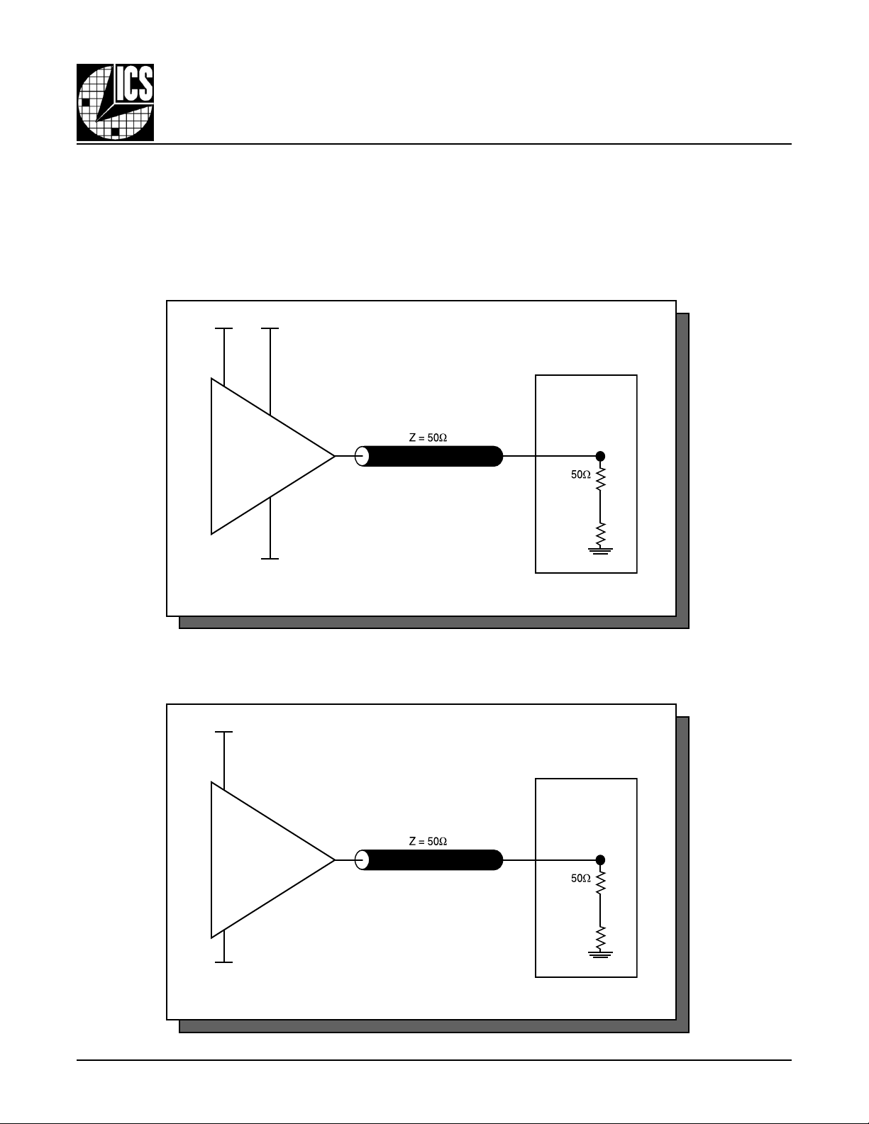
PARAMETER MEASUREMENT INFORMATION
ICS8344-01
LOW SKEW, 1-TO-24
DIFFERENTIAL-TO-L VCMOS FANOUT BUFFER
V
V
DD
DDO
LVCMOS
VDD = +1.65V
V
= 1.65V
DDO
GND = -1.65V
V
DDO
SCOPE
Qx
FIGURE 1A - 3.3V OUTPUT LOAD TEST CIRCUIT
SCOPE
LVCMOS
V
= +1.25V
DDO
GND = -1.25V
FIGURE 1B - 2.5V OUTPUT LOAD TEST CIRCUIT
8344AY-01 www.icst.com/products/hiperclocks.html REV. B AUGUST 6, 2001
8
Qx
Page 9

Integrated
Circuit
Systems, Inc.
CLK0, CLK 1
nCLK0, nCLK1
V
GND
DIFFERENTIAL-TO-L VCMOS FANOUT BUFFER
DD
VPP
FIGURE 2 - DIFFERENTIAL INPUT LEVEL
Cross Points
V
ICS8344-01
LOW SKEW, 1-TO-24
CMR
Qx
Qy
PART 1
PART 2
tsk(o)
FIGURE 3 - OUTPUT SKEW
Qx
Qy
tsk(pp)
FIGURE 4 - PART-TO-PART SKEW
8344AY-01 www.icst.com/products/hiperclocks.html REV. B AUGUST 6, 2001
9
Page 10

Integrated
Circuit
Systems, Inc.
ICS8344-01
LOW SKEW, 1-TO-24
DIFFERENTIAL-TO-L VCMOS FANOUT BUFFER
Clock Inputs
and Outputs
nCLK0, nCLK1
CLK0, CLK1
Q0 - Q23
70%
30%
trise tfall
FIGURE 5 - INPUT AND OUTPUT RISE AND FALL TIME
t
PD
70%
30%
V
SWING
CLK0, CLK1,
Q0 - Q23
nCLK0, nCLK1
FIGURE 6 - PROPAGATION DELAY
Pulse Width
t
PERIOD
t
odc =
PW
t
PERIOD
FIGURE 7 - odc & t
PERIOD
8344AY-01 www.icst.com/products/hiperclocks.html REV. B AUGUST 6, 2001
10
Page 11

Integrated
Circuit
Systems, Inc.
ICS8344-01
LOW SKEW, 1-TO-24
DIFFERENTIAL-TO-L VCMOS FANOUT BUFFER
APPLICATION INFORMATION
WIRING THE DIFFERENTIAL INPUT TO ACCEPT SINGLE ENDED LEVELS
Figure 8
generated by the bias resistors R1, R2 and C1. This bias circuit should be located as close as possible to the input pin. The ratio of
R1 and R2 might need to be adjusted to position the V_REF in the center of the input voltage swing. For example, if the input clock
swing is only 2.5V and V
shows how the differential input can be wired to accept single ended levels. The reference voltage V_REF ~ VDD/2 is
= 3.3V , V_REF should be 1.25V and R2/R1 = 0.609.
DD
CLK_IN
C1
0.1uF
FIGURE 8 - SINGLE ENDED SIGNAL DRIVING DIFFERENTIAL INPUT
R1
1K
V_REF
R2
1K
VDD
+
-
8344AY-01 www.icst.com/products/hiperclocks.html REV. B AUGUST 6, 2001
11
Page 12

Integrated
Circuit
Systems, Inc.
ICS8344-01
LOW SKEW, 1-TO-24
DIFFERENTIAL-TO-L VCMOS FANOUT BUFFER
POWER CONSIDERATIONS
This section provides information on power dissipation and junction temperature for the ICS8344-01.
Equations and example calculations are also provided.
1. Power Dissipation.
The total power dissipation for the ICS8344-01 is the sum of the core power plus the power dissipated in the load(s).
The following is the power dissipation for V
NOTE: Please refer to Section 3 for details on calculating power dissipated in the load.
= 3.3V + 5% = 3.465V , which gives worst case results.
DD
• Power (core)
• Power (outputs)
If all outputs are loaded, the total power is 24* 32mW = 768mW
T otal Power
MAX
= V
MAX
_MAX
* I
DD_MAX
= 32mW/Loaded Output pair
= 3.465V * 95mA = 329.2mW
DD_MAX
(3.465V , with all outputs switching) = 329.2mW + 768mW = 1097.2mW
2. Junction T emperature.
Junction temperature, Tj, is the temperature at the junction of the bond wire and bond pad and directly affects the reliability of the
device. The maximum recommended junction temperature for HiPerClockS
The equation for Tj is as follows: Tj = θ
Tj = Junction T emperature
θ
= junction-to-ambient thermal resistance
JA
Pd_total = T otal device power dissipation (example calculation is in section 1 above)
T
= Ambient T emperature
A
In order to calculate junction temperature, the appropriate junction-to-ambient thermal resistance θ
moderate air flow of 200 linear feet per minute and a multi-layer board, the appropriate value is 42.1°C/W per Table 6 below .
Therefore, Tj for an ambient temperature of 70°C with all outputs switching is:
70°C + 0.1097W * 42.1°C/W = 74.6°C. This is well below the limit of 125°C
This calculation is only an example. Tj will obviously vary depending on the number of loaded outputs, supply voltage, air flow,
and the type of board (single layer or multi-layer).
* Pd_total + T
JA
A
TM
devices is 125°C.
must be used . Assuming a
JA
Table 6. Thermal Resistance qJA for 48-pin LQFP, Forced Convection
q
by Velocity (Linear Feet per Minute)
JA
0 200 500
Single-Layer PCB, JEDEC Standard Test Boards 67.8°C/W 55.9°C/W 50.1°C/W
Multi-Layer PCB, JEDEC Standard Test Boards 47.9°C/W 42.1°C/W 39.4°C/W
NOTE: Most modern PCB designs use multi-layered boards. The data in the second row pertains to most designs.
8344AY-01 www.icst.com/products/hiperclocks.html REV. B AUGUST 6, 2001
12
Page 13

Integrated
Circuit
Systems, Inc.
DIFFERENTIAL-TO-L VCMOS FANOUT BUFFER
3. Calculations and Equations.
The purpose of this section is to derive the power dissipated into the load.
ICS8344-01
LOW SKEW, 1-TO-24
LVCMOS output driver circuit and termination are shown in
Figure 9.
V
DDO
Q1
V
OUT
RL
Ω
50
FIGURE 9 - LVCMOS DRIVER CIRCUIT AND TERMINATION
To calculate worst case power dissipation into the load, use the following equations which assume a 50Ω load, and a termination
voltage of V
Pd_H is power dissipation when the output drives high.
Pd_L is the power dissipation when the output drives low .
DD
- 2V .
Pd_H = (V
Pd_L = (V
OH_MAX /RL
OL_MAX /RL
• For logic high, V
• For logic low, V
) * (V
) * (V
DD_MAX
DD_MAX
OUT
= V
OUT
= V
- V
- V
OH_MAX
OL_MAX
OH_MAX
OL_MAX
= V
)
)
= V
DD_MAX
DD_MAX
– 1.2V
– 0.4V
Pd_H = (1.2V/50Ω) * (2V - 1.2V) = 19.2mW
Pd_L = (0.4V/50Ω) * (2V - 0.4V) = 12.8mW
T otal Power Dissipation per output pair = Pd_H + Pd_L = 32mW
8344AY-01 www.icst.com/products/hiperclocks.html REV. B AUGUST 6, 2001
13
Page 14
Integrated
Circuit
Systems, Inc.
ICS8344-01
LOW SKEW, 1-TO-24
DIFFERENTIAL-TO-L VCMOS FANOUT BUFFER
RELIABILITY INFORMATION
TABLE 7. θ
Single-Layer PCB, JEDEC Standard Test Boards 67.8°C/W 55.9°C/W 50.1°C/W
Multi-Layer PCB, JEDEC Standard Test Boards 47.9°C/W 42.1°C/W 39.4°C/W
NOTE: Most modern PCB designs use multi-layered boards. The data in the second row pertains to most designs.
TRANSISTOR COUNT
The transistor count for ICS8344-01 is: 1503
. AIR FLOW TABLE
VS
JA
q
JA
by V elocity (Linear Feet per Minute)
0 200 500
8344AY-01 www.icst.com/products/hiperclocks.html REV. B AUGUST 6, 2001
14
Page 15
Integrated
Circuit
Systems, Inc.
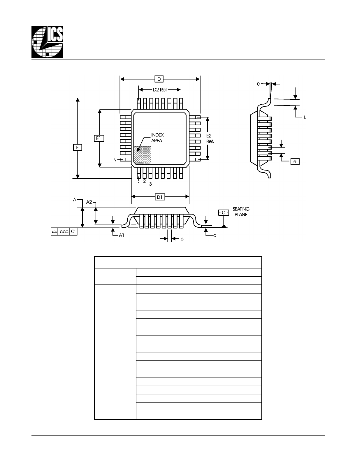
PACKAGE OUTLINE - Y SUFFIX
ICS8344-01
LOW SKEW, 1-TO-24
DIFFERENTIAL-TO-L VCMOS FANOUT BUFFER
TABLE 8. PACKAGE DIMENSIONS
NOITAIRAVCEDEJ
LOBMYS
N
A
1A
2A
b
c
D
1D
2D
E
1E
2E
e
L
q
ccc
Reference Document: JEDEC Publication 95, MS-026
MUMINIMLANIMONMUMIXAM
----06.1
50.0--51.0
53.104.154.1
71.022.072.0
90.0--02.0
54.006.057.0
0
°
----80.0
SRETEMILLIMNISNOISNEMIDLLA
CBB
84
CISAB00.9
CISAB00.7
.feR05.5
CISAB00.9
CISAB00.7
.feR05.5
CISAB05.0
--
7
°
8344AY-01 www.icst.com/products/hiperclocks.html REV. B AUGUST 6, 2001
15
Page 16

Integrated
Circuit
Systems, Inc.
TABLE 9. ORDERING INFORMATION
rebmuNredrO/traPgnikraMegakcaPtnuoCerutarepmeT
10-YA4438SCI10-YA4438SCIPFQLdaeL84yartrep052C°07otC°0
T10-YA4438SCI10-YA4438SCIleeRdnaepaTnoPFQLdaeL840001C°07otC°0
ICS8344-01
LOW SKEW, 1-TO-24
DIFFERENTIAL-TO-L VCMOS FANOUT BUFFER
While the information presented herein has been checked for both accuracy and reliability, Integrated Circuit Systems, Incorporated (ICS) assumes no responsibility for either its use
or for infringement of any patents or other rights of third parties, which would result from its use. No other circuits, patents, or licenses are implied. This product is intended for use
in normal commercial applications. Any other applications such as those requiring extended temperature range, high reliability, or other extraordinary environmental requirements are
not recommended without additional processing by ICS. ICS reserves the right to change any circuitry or specifications without notice. ICS does not authorize or warrant any ICS
product for use in life support devices or critical medical instruments.
8344AY-01 www.icst.com/products/hiperclocks.html REV. B AUGUST 6, 2001
16
 Loading...