

Page 1
ICS674-01
User Configurable Divider
MDS 674-01 A 1 Revision 033199 Printed 11/15/00
Integrated Circuit Systems • 525 Race Street • San Jose • CA • 95126 •(408)295-9800tel•(408)295-9818fax
PRELIMINARY INFORMATION
• Packaged as 28 pin SSOP (150 mil body)
• Supports ICS673 PLL Building Block
• User determines the divide by setting input pins
• Pull-ups on all select inputs
• Includes one 7-bit Divider for OUTA
• Includes one 9-bit Divider and one selectable
Post Divider for OUTB
• Operating voltages of 3.3 V or 5.0 V
• Industrial temperature range available
• 25mA drive capability at TTL levels
• Advanced, low power CMOS process
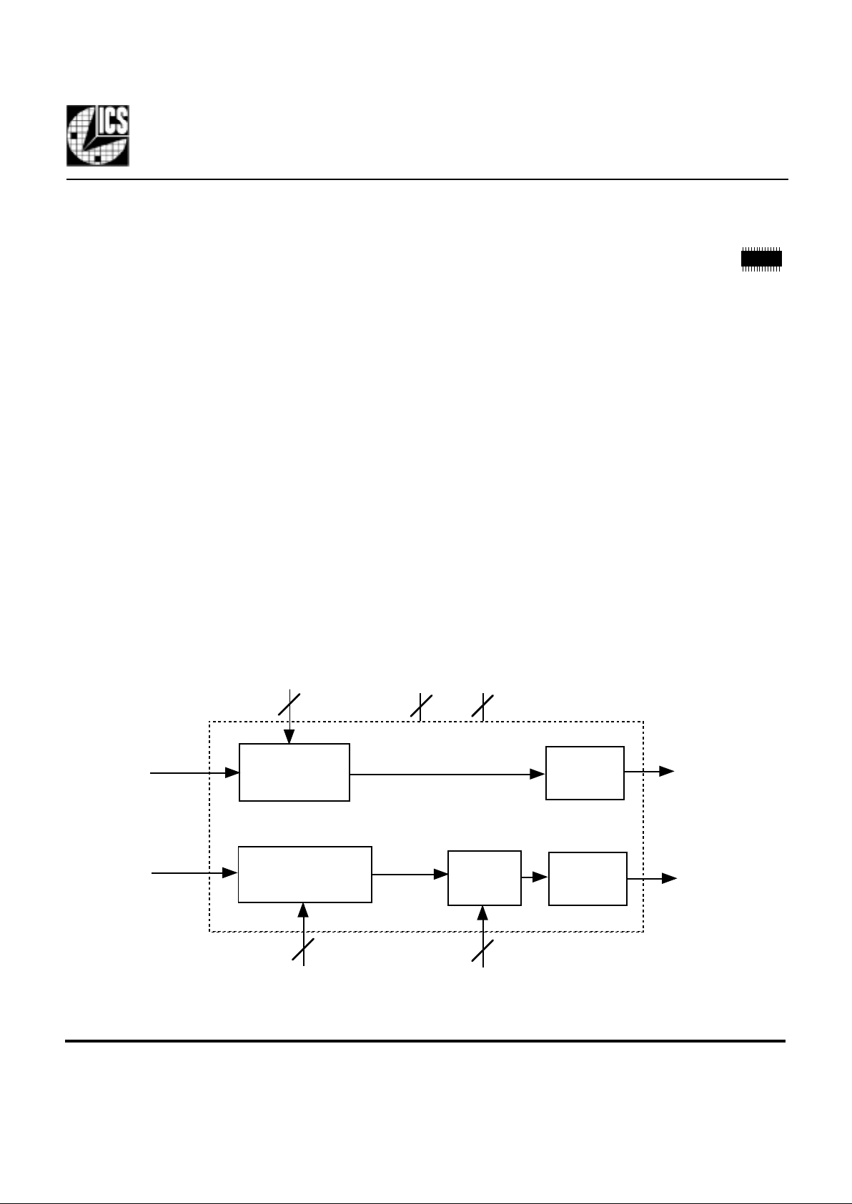
The ICS674-01 consists of 2 separate
configurable dividers. The A Divider is a 7 bit
divider and can divide by 3 to 129. The
B Divider consists of a 9 bit divider followed by a
post divider. The 9 bit divider can divide by 12
to 519. The post divider has eight settings of
1, 2, 4, 5, 6, 7, 8 and 10 giving a maximum total
divide of 5190. The A and B Dividers can be
cascaded to give a maximum divide of 669510.
The ICS674-01 supports the ICS673 PLL
Building Block and enables the user to build a full
custom PLL synthesizer.
Block Diagram
Description
Features
Divider A
(7-Bit)
Output
Buffer
Post
Divider
Divider B
(9-Bit)
7
2
3
VDD GND
INA
INB
OUTA
OUTB
B8:B0
A6:A0
93
S2:S0
Output
Buffer
Page 2
ICS674-01
User Configurable Divider
MDS 674-01 A 2 Revision 033199 Printed 11/15/00
Integrated Circuit Systems • 525 Race Street • San Jose • CA • 95126 •(408)295-9800tel•(408)295-9818fax
PRELIMINARY INFORMATION
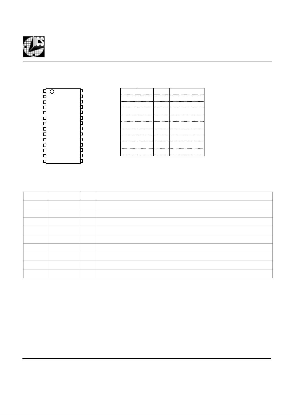
Pin Assignment
Key: I(PU) = Input with internal pull-up resistor; I=Input (no pull-up); O = Output;
P = Power su
pp
ly connection
1
8
9
2
3
4
5
6
7
10
11
12
13
14
16
15
20
17
18
19
25
24
23
22
21
26
27
28
B2
INB
VDD
INA
GND
B4
VDD
OUTA
GND
A2
A4
B8
OUTB
A3
A1
B6
B5
GND
A0
Pin # Name Type Description
1, 2, 24-28 A5, A6, A0-A4 I(PU) Divider A word input pins. Forms a binary number from 3 to 129.
3, 4, 5 S0, S1, S2 I(PU) Select pins for Post Divider. See table above.
6, 23 VDD P Connect to VDD.
7 INA I Divider A input.
8 INB I Divider B input.
9, 19, 20 GND P Connect to ground.
10-18 B0-B8 I(PU) Divider B word input pins. Forms a binary number from 12 to 519.
21 OUTB O Divider B output.
22 OUTA O Divider A output.
A5
A6
B0
B3
B1
S2
S0
S1
B7
S2 S1 S0 Post
pin 5 pin 4 pin 3 Divide
000 10
001 2
010 8
011 4
100 5
101 7
110 1
111 6
Post Divider Table
Pin Description
External Components
The ICS674-01 requires a 0.01µF decoupling capacitor to be connected between VDD and GND. It
must be connected close to the ICS674-01 to minimize lead inductance. Terminating resistors of 33Ω can
be used in series with the OUTA and OUTB
p
ins.
Page 3

ICS674-01
User Configurable Divider
MDS 674-01 A 3 Revision 033199 Printed 11/15/00
Integrated Circuit Systems • 525 Race Street • San Jose • CA • 95126 •(408)295-9800tel•(408)295-9818fax
PRELIMINARY INFORMATION
Determining (setting) the divider
The user has full control in setting the desired divide. The user should connect the appropriate divider select
input pins directly to ground (or VDD, although this is not required because of internal pull-ups) during
Printed Circuit Board layout, so that the ICS674-01 automatically produces the correct divide when all
components are soldered. It is also possible to connect the inputs to parallel I/O ports in order to change
divides.
The divides of the ICS674-01 can be determined by the following simple equations:
Divide A = DAW+2
Where Divider A Word (DAW) = 1 to 127 (0 is not permitted).
Divide B = (DBW+8)•PD
Where Divider B Word (DBW) = 4 to 511 (0,1,2,3, are not permitted).
Post Divider (PD) = values on Page 2
For example, suppose Divide A is desired to be 61 and Divide B is desired to be 284, then
DAW = 59, DBW = 276 and PD = 1. This means A6:A0 is 0111011, B8:B0 is
100010100 and S2:S0 is 110. Since all inputs have pull-ups, it is only necessary to ground
the zero pins, namely A6, A2, B7, B6, B5, B3, B1, B0 and S0.
Page 4

ICS674-01
User Configurable Divider
MDS 674-01 A 4 Revision 033199 Printed 11/15/00
Integrated Circuit Systems • 525 Race Street • San Jose • CA • 95126 •(408)295-9800tel•(408)295-9818fax
PRELIMINARY INFORMATION
Output
Clock
Divide A
REFIN
FBIN
ICS673-01
CLK1
CLK2
Divide B
Post
Divide
Reference
Clock
If the reference is in the kHz range, for example 8 kHz, the following configuration may be more
ty
p
ical:
Output
Clock
Divide A
REFIN
FBIN
ICS673-01
CLK1
CLK2
Divide B
Post
Divide
Reference
Clock
Note that in both examples Divide B is connected to the output of the ICS673. This is because Divide B
has a hi
g
her operating frequency than Divide A.
Using the ICS674-01 with the ICS673-01:
The ICS674-01 may be used with the ICS673-01 to build a frequency synthesizer. The following example
shows a ty
p
ical application when the reference clock is in the MHz range:
ICS674-01
ICS674-01
Page 5

ICS674-01
User Configurable Divider
MDS 674-01 A 5 Revision 033199 Printed 11/15/00
Integrated Circuit Systems • 525 Race Street • San Jose • CA • 95126 •(408)295-9800tel•(408)295-9818fax
PRELIMINARY INFORMATION
Parameter Conditions Minimum Typical Maximum Units
ABSOLUTE MAXIMUM RATINGS (stresses beond these can permanentl damage the device)
Supply Voltage, VDD Referenced to GND 7 V
Inputs Referenced to GND -0.5 VDD+0.5 V
Clock Output Referenced to GND -0.5 VDD+0.5 V
Ambient Operating Temperature 0 70 °C
Ambient Operating Temperature I version -40 85 °C
Soldering Temperature Max of 10 seconds 260 °C
Storage Temperature -65 150 °C
DC CHARACTERISTICS (VDD = 5.0V unless otherwise noted)
Operating Voltage, VDD 3 5.5 V
Input High Voltage, VIH All A, B, and S pins 2 V
Input Low Voltage, VIL All A, B, and S pins 0.8 V
Input High Voltage, VIH, INA and INB only (VDD/2)+1 VDD/2 V
Input Low Voltage, VIL, INA and INB only VDD/2 (VDD/2)-1 V
Output High Voltage, VOH IOH=-25mA 2.4 V
Output Low Voltage, VOL IOL=25mA 0.4 V
IDD, Op. Supply Cur., DivA=DivB=20 at 3.3 V No Load, fin=100 MHz 3 mA
IDD, Op. Supply Cur., DivA=DivB=20 at 5 V No Load, fin=100 MHz
5
mA
Short Circuit Current, outputs ±70 mA
On-Chip Pull-up Resistor A, B, S select pins 270 kΩ
Input Capacitance A, B, S select pins 5 pF
AC CHARACTERISTICS (VDD = 5.0V unless otherwise noted)
Input Frequency, Divider A at 3.3 V 0 135 MHz
Input Frequency, Divider B at 3.3 V 0 180 MHz
Input Frequency, Divider A at 5 V 0 200 MHz
Input Frequency, Divider B at 5 V 0 235 MHz
Input Frequency, Divider A (Industrial temperature) at 3.3 V at 85 °C 0 125 MHz
Input Frequency, Divider B (Industrial temperature) at 3.3 V at 85 °C 0 170 MHz
Input Frequency, Divider A (Industrial temperature) at 5 V at 85 °C 0 190 MHz
Input Frequency, Divider B (Industrial temperature) at 5 V at 85 °C 0 220 MHz
Output Clock Rise Time 0.8 to 2.0V 1 ns
Output Clock Fall Time 2.0 to 0.8V 1 ns
OUTB Clock Duty Cycle (see note) at VDD/2 45 49 to 51 55 %
OUTB Clock Duty Cycle, odd post dividers at VDD/2, except PD=1 40 60 %
OUTA Clock Duty Cycle (see note) at VDD/2 20 98.5 %
Note:
The duty cycle of OUTA is dependent on the selected divide. This is because OUTA goes low for 2 input
clock cycles on INA. So, for example, if a divide of 20 is selected, the duty cycle will be 90%.
Similarly, if PD=1 is selected for OUTB, the duty cycle will be dependent on the selected divide. In this
case OUTB
g
oes high for approximately 8 input clock cycles on INB.
Page 6

ICS674-01
User Configurable Divider
MDS 674-01 A 6 Revision 033199 Printed 11/15/00
Integrated Circuit Systems • 525 Race Street • San Jose • CA • 95126 •(408)295-9800tel•(408)295-9818fax
PRELIMINARY INFORMATION
While the information presented herein has been checked for both accuracy and reliability, ICS assumes no responsibility for either its use or for the infringement of any patents or
other rights of third parties, which would result from its use. No other circuits, patents, or licenses are implied. This product is intended for use in normal commercial applications.
Any other applications such as those requiring extended temperature range, high reliability, or other extraordinary environmental requirements are not recommended without
additional processing by ICS. ICS reserves the right to change any circuitry or specifications without notice. ICS does not authorize or warrant any ICS product for use in life
support devices or critical medical instruments.
Package Outline and Package Dimensions
b
D
EH
e
Q
c
h x 45°
L
28 pin SSOP
Inches Millimeters
Symbol Min Max Min Max
A 0.061 0.068 1.55 1.73
b 0.008 0.012 0.203 0.305
c 0.007 0.010 0.191 0.254
D 0.385 0.400 9.779 10.160
E 0.150 0.160 3.810 4.064
H 0.230 0.245 5.842 6.223
e .025 B
S
S
C 0.635 BSC
h 0.016 0.406
Q 0.004 0.01 0.102 0.254
L 0.016 0.035 0.406 0.889
Ordering Information
Part/Order Number Marking * Package Temperature
ICS674R-01 674R-01 28 pin narrow SSOP 0 to 70 °C
ICS674R-01T 674R-01 28 pin SSOP on tape and reel 0 to 70 °C
ICS674R-01I 674R-01I 28 pin narrow SSOP -40 to 85 °C
ICS674R-01IT 674R-01I 28 pin SSOP on tape and reel -40 to 85 °C
*This shows the top line marking. The part will have the letters ICS in a box on the upper left
hand corner.
 Loading...