

Page 1
Low Phase Noise Zero Delay Buffer and Multiplier
p
Description Features
The ICS670-01 is a high speed, low phase noise
Zero Delay Buffer (ZDB) which integrates ICS’
proprietary analog/digital Phase Locked Loop
(PLL) techniques. Part of ICS’ ClockBlocks
family, the zero delay feature means that the rising
edge of the input clock aligns with the rising edges
of the outputs, giving the appearance of no delay
through the device. There are two identical outputs
on the chip. The FBCLK should be used to
connect to the FBIN. Each output has its own
output enable pin.
™
• Packaged in 16 pin SOIC
• Clock inputs from 5 to 160 MHz (see page 2)
• Patented PLL with the lowest phase noise
• Output clocks up to 160 MHz at 3.3 V
• 15 selectable on-chip multipliers
• Power down mode available
• Low phase noise: -124 dBc/Hz at 10 kHz
• Output Enable function tri-states outputs
ICS670-01
The chip is ideal for synchronizing outputs in a
large variety of systems, from personal computers
to data communications to video. By allowing offchip feedback paths, the ICS670-01 can eliminate
the delay through other devices. The 15 different
on-chip multipliers work in a variety of
applications. For other multipliers, including
fractional multipliers, see the ICS527.
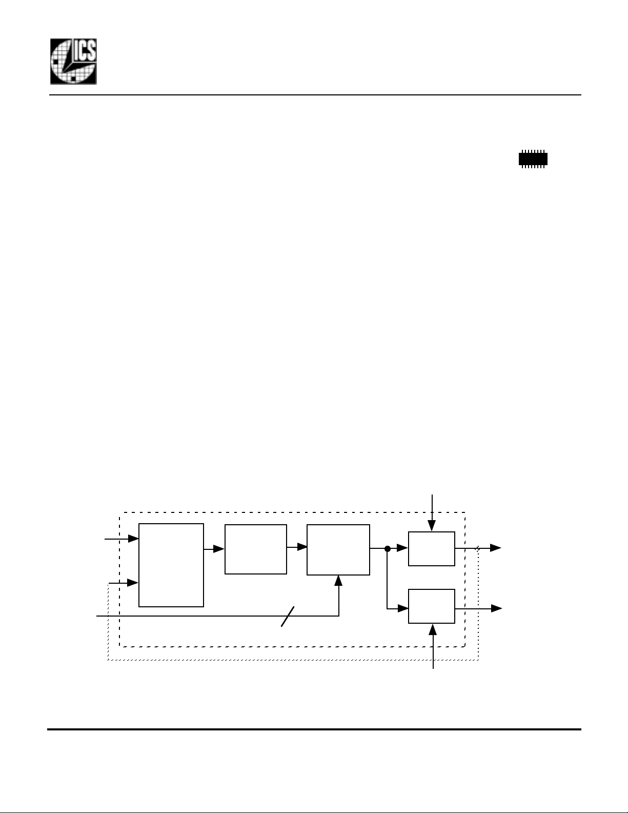
Block Diagram
ICLK
FBIN
S3:S0
Phase
Detector,
Charge
Pump, and
Loop Filter
Voltage
Controlled
Oscillator
4
• Low jitter 15 ps one sigma
• Full swing CMOS outputs with 25 mA drive
capability at TTL levels
• Advanced, low power, sub-micron CMOS process
• Industrial temperature version available
• 3.3 V or 5 V operation
OE1
ROM-
Based
Multi
liers
Output
Buffer
Output
Buffer
FBCLK
CLK2
External feedback from FBCLK is recommended.
MDS 670-01 B 1 Revision 100900 Printed 11/15/00
Integrated Circuit Systems • 525 Race Street • San Jose •CA•95126•(408) 295-9800tel•http://www.icst.com
OE2
Page 2
ICS670-01
Low Phase Noise Zero Delay Buffer and Multiplier
Pin Assignment
VDD
VDD
VDD
CLK2
OE2
FBCLK
OE1
FBIN
1
2
3
4
5
6
7
8
ICS670-01
Pin Descriptions
16
15
14
13
12
11
10
Multiplier Select Table
S3 S2 S1 S0 CLK2 (and FBCLK) Input Range (MHz)
GND
GND
GND
S0
S1
S2
S3
ICLK
9
0000 Low (Power down entire chip) 0001 Input x1.333 18 - 12 0
0010 Input x6 5 - 26.67
0011 Input x1.5 16.67 - 107
0100 Input x3.333 7.5 - 48
0101 Input x2.50 10 - 6 4
0110 Input x4 6 - 4 0
0111 Input x1 25 - 1 6 0
1000 Input x2.333 11 - 6 9
1001 Input x2.666 10 - 6 0
1010 Input x12 5 - 13.33
1011 Input x3 8 - 53.33
1100 Input x10 5 - 16
1101 Input x5 6 - 32
1110 Input x8 5 - 20
1111 Input x2 12 - 8 0
0=connect directly to ground
1=connect directl to VDD
Number Name Type Description
1 VDD P Connect to +3.3V or +5V. Must match other VDDs.
2 VDD P Connect to +3.3V or +5V. Must match other VDDs.
3 VDD P Connect to +3.3V or +5V. Must match other VDDs.
4 CLK2 O Clock output from VCO. Output frequency equals the input frequency times multiplier.
5 OE2 I Output clock enable 2. Tri-states the clock 2 output when low.
6 FBCLK O Clock ouput from VCO. Output frequency equals the input frequency times multiplier.
7
8 FBIN CI Feedback clock input.
9 ICLK CI Clock input. Connect to a 5 - 160 MHz clock.
10 S3 I Multiplier select pin 3. Determines outputs per table above. Internal pull-up.
11 S2 I Multiplier select pin 2. Determines outputs per table above. Internal pull-up.
12 S1 I Multiplier select pin 1. Determines outputs per table above. Internal pull-up.
13 S0 I Multiplier select pin 0. Determines outputs per table above. Internal pull-up.
14 GND P Connect to ground.
15 GND P Connect to ground.
16 GND P Connect to ground.
OE1 I Output clock enable 1. Tri-states the feedback clock output when low.
Key: I = Input with internal pull-up resistor; O = output; P = power supply connection; CI = clock input.
MDS 670-01 B 2 Revision 100900 Printed 11/15/00
Integrated Circuit Systems • 525 Race Street • San Jose •CA•95126•(408) 295-9800tel•http://www.icst.com
Page 3

ICS670-01
V
V
Low Phase Noise Zero Delay Buffer and Multiplier
Electrical Specifications
Parameter Conditions Minimum Typical Maximum Units
ABSOLUTE MAXIMUM RATINGS (note 1)
Supply voltage, VDD Referenced to GND 7 V
Inputs and Clock Outputs Referenced to GND -0.5 VDD+0.5 V
Ambient Operating Temperature 0 70 °C
Ambient Operating Temperature, ICS670M-01I Industrial temperature -40 85 °C
Soldering Temperature Max of 10 seconds 260 °C
Storage temperature -65 150 °C
DC CHARACTERISTICS (VDD = 3.3 V unless noted)
Operating Voltage, VDD 3.0 5.5 V
Input High Voltage, VIH 2 V
Input Low Voltage, VIL 0.8 V
Output High Voltage, VOH, CMOS level IOH=-4mA VDD-0.4 V
Output High Voltage, VOH IOH=-12mA 2.4 V
Output Low Voltage, VOL IOL=12mA 0.4 V
Operating Supply Current, IDD No Load 35 mA
Short Circuit Current Each output ±50 mA
Internal Pull-up Resistor OE, select pins 200 kΩ
Input Capacitance OE, select pins 5 pF
AC CHARACTERISTICS (VDD = 3.3
Input Frequency (see table on page 2) Depends on multiplier 5 160 MHz
Output Frequency at 3.3V or 5V 160 MHz
Output Clock Rise Time 0.8 to 2.0V, no load 1.5 ns
Output Clock Fall Time 0.8 to 2.0V, no load 1.5 ns
Output Clock Duty Cycle At VDD/2 45 50 55 %
Input to output skew, rising edges Note 2 ±100 ps
Maximum Absolute Jitter, short term ±45 ps
Maximum Jitter, one sigma 15 ps
Phase Noise, relative to carrier, 125 MHz (x5) 100 Hz offset -110 dBc/Hz
Phase Noise, relative to carrier, 125 MHz (x5) 1 kHz offset -122 dBc/Hz
Phase Noise, relative to carrier, 125 MHz (x5) 10 kHz offset -121 dBc/Hz
Phase Noise, relative to carrier, 125 MHz (x5) 100 kHz offset -117 dBc/Hz
unless noted)
Notes: 1. Stresses beyond those listed under Absolute Maximum Ratings could cause permanent damage to the device. Prolonged
exposure to levels above the operating limits but below the Absolute Maximums may affect device reliability.
2. Rising edge of ICLK compared with rising edge of CLK2, with FBCLK connected to FBIN, and 15 pF load on CLK2.
See the graph on page 4 for skew versus frequency and loading.
MDS 670-01 B 3 Revision 100900 Printed 11/15/00
Integrated Circuit Systems • 525 Race Street • San Jose •CA•95126•(408) 295-9800tel•http://www.icst.com
Page 4

300
p
ICS670-01
Low Phase Noise Zero Delay Buffer and Multiplier
200
100
0
0 2 5 50 75 100 125 150
-100
Skew (ps)
-200
-300
-400
CL = 20 pF
CL = 10 pF
CLK2 Frequency (MHz)
Figure 1. ICS670-01 skew from ICLK to CLK2, with change in load capacitance.
VDD = 3.3 V.
Adjusting Input/Output Skew
The data in Figure 1 can be used to adjust individual circuit characteristics and achieve the minimum
possible skew between ICLK and CLK2. With a 125 MHz output, for example, having a total load
capacitance of 15 pF will result in nearly zero skew between ICLK and CLK2. Note that the load
capacitance includes board trace capacitance, input capacitance of the load being driven by the ICS670-01,
and any additional ca
acitors connected to CLK2.
0
-20
-40
-60
-80
Phase Noise (dBc/Hz)
-100
-120
-140
10.0E+0 100.0E+0 1.0E+3 10.0E+3 100.0E+3 1.0E+6 10.0E+6
Offset from Carrier (Hz)
Figure 2. Phase Noise of ICS670-01 at 125 MHz out, 25 MHz clock input.
VDD = 3.3 V.
MDS 670-01 B 4 Revision 100900 Printed 11/15/00
Integrated Circuit Systems • 525 Race Street • San Jose •CA•95126•(408) 295-9800tel•http://www.icst.com
Page 5

ICS670-01
p
S
S
Low Phase Noise Zero Delay Buffer and Multiplier
External Components Selection
The ICS670-01 requires a minimum number of external components for proper operation. Decoupling
capacitors of 0.01 µF should be connected between VDD and GND, as close to the part as possible. A
series termination resistor of 33 Ω may be used for each clock out
Package Outline and Package Dimensions
(
For current dimensional specifications, see JEDEC Publication No. 95.)
EH
INDEX
AREA
1
h x 45°
D
ut.
16 pin SOIC narrow
Inches Millimeters
Symbol Min Max Min Max
A 0.0532 0.0688 1.35 1.75
A1
D 0.3859 0.3937 9.80 10.00
H 0.2284 0.2440 5.80 6.20
0.0040 0.0098 0.10 0.24
B 0.0130 0.0200 0.33 0.51
C
0.0075 0.0098 0.19 0.24
E 0.1497 0.1574 3.80 4.00
e .050 BSC 1.27 B
h 0.0099 0.0195 0.25 0.50
L 0.0160 0.0500 0.41 1.27
C
A1
e
C
B
A
L
Ordering Information
Part/Order Number Marking Shipping packaging Package Temperature
ICS670M-01 ICS670M-01 tubes 16 pin narrow SOIC 0 to 70 °C
ICS670M-01T ICS670M-01 tape and reel 16 pin narrow SOIC 0 to 70 °C
ICS670M-01I ICS670M-01I tubes 16 pin narrow SOIC -40 to 85 °C
ICS670M-01IT ICS670M-01I tape and reel 16 pin narrow SOIC -40 to 85 °C
While the information presented herein has been checked for both accuracy and reliability, Integrated Circuit Systems, Incorporated (ICS) assumes no responsibility for either its
use or for the infringement of any patents or other rights of third parties, which would result from its use. No other circuits, patents, or licenses are implied. This product is
intended for use in normal commercial applications. Any other applications such as those requiring extended temperature range, high reliability, or other extraordinary
environmental requirements are not recommended without additional processing by ICS. ICS reserves the right to change any circuitry or specifications without notice. ICS does
not authorize or warrant any ICS product for use in life support devices or critical medical instruments.
MDS 670-01 B 5 Revision 100900 Printed 11/15/00
Integrated Circuit Systems • 525 Race Street • San Jose •CA•95126•(408) 295-9800tel•http://www.icst.com
 Loading...