

Page 1
p
PRELIMINARY INFORMATION
HDTV Set-Top Clock Source
ICS627-01
Description
The ICS627-01 is a low cost, low jitter, high
performance clock synthesizer which can generate
frequencies required for HDTV receivers and settop boxes. Using ICS’s patented analog/digital
Phase-Locked Loop (PLL) techniques, the device
uses an inexpensive fundamental 27 MHz crystal
input to produce low jitter HDTV pixel clocks. It
has a separate input for a 1001/1000 or
2(1001/1000) conversion from a 13.5 MHz,
27 MHz or 54 MHz in
ut.
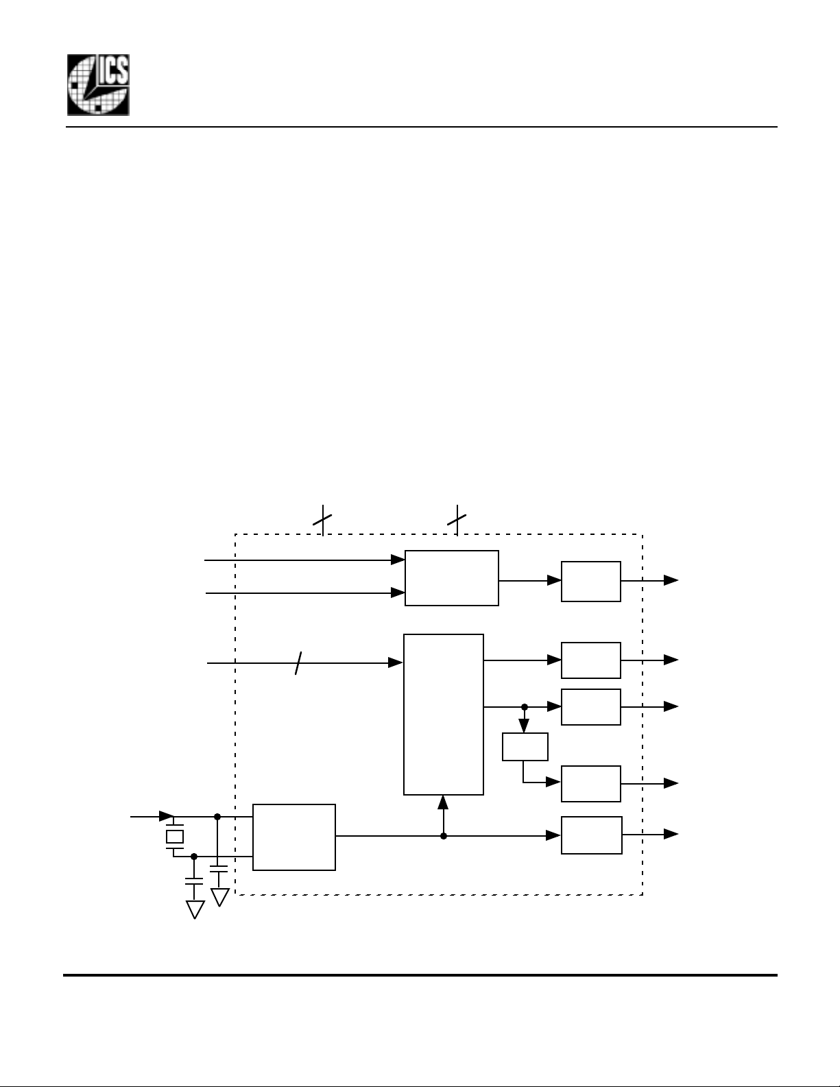
Block Diagram
VDD
Features
• Packaged in 28 pin SSOP (QSOP)
• HDTV frequencies of 74.25 and 74.175824 MHz
• Provides selectable B clock for 27.027 MHz or
other 1001/1000
• Uses a fundamental 27 MHz crystal or clock input
• All frequencies are generated exactly (zero ppm
synthesis error)
• Full CMOS output swings with 12 mA output
drive capability at TTL levels
• Advanced, low power, sub-micron CMOS process
• 3.3 V ±5% operating supply
GND
CLKIN
27.0 MHz
crystal or
clock
input
SB
SA2:0
X1/ICLK
X2
6
Crystal
Oscillator
x1001/1000
PLL
PLL
Clock
Synthesis
Circuitry
÷2
Output
Buffer
Output
Buffer
Output
Buffer
Output
Buffer
Output
Buffer
CLKB
CLKA
CLKC
(54 MHz)
CLKC/2
(27 MHz)
REFOUT
(27 MHz)
MDS 627-01 B 1 Revision 051600
Integrated Circuit Systems, Inc. • 525 Race Street • San Jose •CA•95126•(408) 295-9800tel • www.icst.com
Page 2
PRELIMINARY INFORMATION
j
HDTV Set-Top Clock Source
ICS627-01
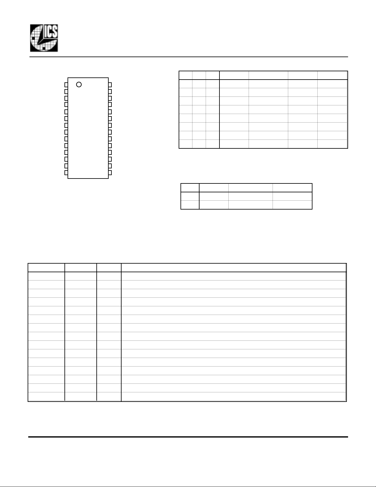
Pin Assignment
1
SA2
2
X2
3
X1
VDD
VDD
CLKIN
VDD
VDD
VDD
GND
GND
CLKC/2
CLKC
CLKB
4
5
6
7
8
9
10
11
12
13
14
28
27
26
25
24
23
22
21
20
19
18
17
16
15
SA2
SA0
SA0
REFOUT
GND
CLKA
VDD
GND
GND
GND
GND
SB
SA1
SA1
CLKA/CLKC Select Table (MHz)
SA2 SA1 SA0 Input CLKA CLKC CLKC/2
0 0 0 27.0 108.0 54.0 27.0
0 0 1 27.0 74.175824* TEST TEST
0 1 0 27.0 54.0 54.0 27.0
0 1 1 27.0 74.25* 54.0 27.0
1 0 0 TEST
1 0 1 27.0 74.175824 54.0 27.0
1 1 0 TEST
1 1 1 27.0 74.250 54.0 27.0
* These selections are recommended for the lowest
itter
CLKB Select Table (MHz)
SB CLKIN CLKB Multiplier
0 13.5 27.027 2002/1000
1 27 - 54 27.027 - 54.054 1001/1000
0 = connect directly to GND
1 = connect directl to VDD
Pin Descriptions
Number Name Type Description
1, 28 SA2 I Pins 1, 28 should be connected together. Selects CLKA and CLKC frequencies. Internal p-u.
2X2XOConnect to a fundamental 27.0 MHz crystal or leave unconnected for clock.
3 X1/ICLK XI Connect to a fundamental 27.0 MHz crystal or clock input.
4, 5, 7-9, 22 VDD P Connect to 3.3V.
6 CLKIN CI Clock input to produce 1001/1000 or 2(1001/1000) at CLKB. See table above.
10, 11, 18, 19 GND P Connect to ground.
12 CLKC/2 O C Clock output divided-by-2. See table above.
13 CLKC O C Clock output. See above table.
14 CLKB O B Clock output. See above table.
15, 16 SA1 I Pins 15, 16 should be connected together. Selects CLKA and CLKC frequencies. Internal p-u.
17 SB I B Clock Select. Selects CLKB frequency. See above table. Internal pull-up.
20, 21, 24 GND P Connect to ground.
23 CLKA O A Clock output. See above table.
25 REFOUT O 27 MHz Reference Output.
26, 27 SA0 I Pins 26, 27 should be connected together. Selects CLKA and CLKC frequencies. Internal p-u.
Key: I = Input; O = output; P = power supply connection; XI, XO = crystal connections; CI = clock input
MDS 627-01 B 2 Revision 051600
Integrated Circuit Systems, Inc. • 525 Race Street • San Jose •CA•95126•(408) 295-9800tel • www.icst.com
Page 3

PRELIMINARY INFORMATION
ICS627-01
HDTV Set-Top Clock Source
Electrical Specifications
Parameter Conditions Minimum Typical Maximum Units
ABSOLUTE MAXIMUM RATINGS (note 1)
Supply voltage, VDD Referenced to GND 7 V
Inputs and Clock Outputs Referenced to GND -0.5 VDD+0.5 V
Ambient Operating Temperature 0 70 °C
Soldering Temperature Max of 10 seconds 260 °C
Storage temperature -65 150 °C
DC CHARACTERISTICS (VDD = 3.3V unless noted)
Operating Voltage, VDD 3.15 3.30 3.45 V
Input High Voltage, VIH 2 V
Input Low Voltage, VIL 0.8 V
Input High Voltage, VIH, ICLK and CLKIN (VDD/2)+1 VDD/2 V
Input Low Voltage, VIL, ICLK and CLKIN VDD/2 (VDD/2)-1 V
Output High Voltage, VOH IOH=-12mA 2.4 V
Output Low Voltage, VOL IOL=12mA 0.4 V
Output High Voltage, VOH, CMOS level IOH=-8mA VDD-0.4 V
Operating Supply Current, IDD No Load, note 2 TBD mA
Short Circuit Current Each output ±50 mA
Input Capacitance 7 pF
Frequency synthesis error All clocks 0 ppm
AC CHARACTERISTICS (VDD = 3.3V unless noted)
Input Frequency 27.0 MHz
Output Clock Rise Time 0.8 to 2.0V 1.5 ns
Output Clock Fall Time 2.0 to 0.8V 1.5 ns
Output Clock Duty Cycle At VDD/2 40 60 %
Maximum Absolute Jitter, short term TBD ps
Notes: 1. Stresses beyond those listed under Absolute Maximum Ratings could cause permanent damage to the device. Prolonged
exposure to levels above the operating limits but below the Absolute Maximums may affect device reliability.
2. With all clocks at highest MHz.
External Components
The ICS627-01 requires a minimum number of external components for proper operation. Use a low
inductance ground plane, connect all GNDs to this. Connect 0.01µF decoupling caps across pins 5 and 10, 8
and 10, and 22 and 20, as close to the ICS627-01 as possible. A series termination resistor of 33 Ω may be
used for each clock output. The 27.000 MHz crystal must be connected as close to the chip as possible. The
crystal should be a fundamental mode, parallel resonant. Crystal capacitors should be connected from pins X1
to ground and X2 to ground. The value of these capacitors is given by the following equation, where C
crystal load capacitance: Crystal caps (pF) = (CL-6) x 2. So for a crystal with 16pF load capacitance, two 20pF
caps should be used. If a clock input is used, drive it into X1 and leave X2 unconnected.
MDS 627-01 B 3 Revision 051600
Integrated Circuit Systems, Inc. • 525 Race Street • San Jose •CA•95126•(408) 295-9800tel • www.icst.com
is the
L
Page 4

PRELIMINARY INFORMATION
HDTV Set-Top Clock Source
Package Outline and Package Dimensions
(
For current dimensional specifications, see JEDEC Publication No. 95.)
28 pin SSOP
Symbol Min Max Min Max
A 0.053 0.069 1.35 1.75
A1 0.004 0.010 0.10 0.25
b 0.008 0.012 0.20 0.30
c 0.007 0.010 0.19 0.25
D 0.386 0.394 9.80 10.01
e .025 BSC 0.635 BSC
E 0.228 0.244 5.79 6.20
E1 0.150 0.157 3.81 3.99
L 0.016 0.050 0.41 1.27
INDEX
AREA
E1 E
12
D
ICS627-01
Inches Millimeters
A1
e
b
c
L
Ordering Information
Part/Order Number Marking Shipping packaging Package Temperature
ICS627R-01 ICS627R-01 tubes 28 pin SSOP (QSOP) 0-70 °C
ICS627R-01T ICS627R-01 tape and reel 28 pin SSOP (QSOP) 0-70 °C
While the information presented herein has been checked for both accuracy and reliability, Integrated Circuit Systems (ICS) assumes no responsibility for either its use or for the
infringement of any patents or other rights of third parties, which would result from its use. No other circuits, patents, or licenses are implied. This product is intended for use in
normal commercial applications. Any other applications such as those requiring extended temperature range, high reliability, or other extraordinary environmental requirements
are not recommended without additional processing by ICS. ICS reserves the right to change any circuitry or specifications without notice. ICS does not authorize or warrant any
ICS product for use in life support devices or critical medical instruments.
A
MDS 627-01 B 4 Revision 051600
Integrated Circuit Systems, Inc. • 525 Race Street • San Jose •CA•95126•(408) 295-9800tel • www.icst.com
 Loading...