

Page 1
PRELIMINARY INFORMATION
ICS614-01
ICRO
C
LOCK
Description
The ICS614-01 is a low cost, low jitter, high
performance clock synthesizer for Intel’s i752
graphics systems. It includes frequencies for video
encoders and decoders. Using analog PhaseLocked Loop (PLL) techniques, the device accepts
a 27 MHz fundamental mode crystal or clock
input to produce multiple output clocks. The chip
provides highly accurate video encoder and
decoder clocks, as well as the 48 MHz necessary
for the Intel graphics processor, and can produce a
24.576 MHz audio clock.
See the ICS604 or ICS513 for 8 pin devices that
supply 48 MHz from a 14.31818 MHz input.
16 pin Intel Graphics Clock Source
Features
• Packaged in 16 pin SOIC
• Uses fundamental 27 MHz input crystal
• Supports Intel i752 graphics chip, popular video
encoders and decoders, and audio
• Low jitter - 50 ps one sigma
• Output Enable function tri-states outputs
• 25mA output drive capability at TTL levels
• Advanced, low power, sub-micron CMOS process
• 5V±10% core voltage. Inputs and outputs can run
3.3V (or 5V) for easy system interface
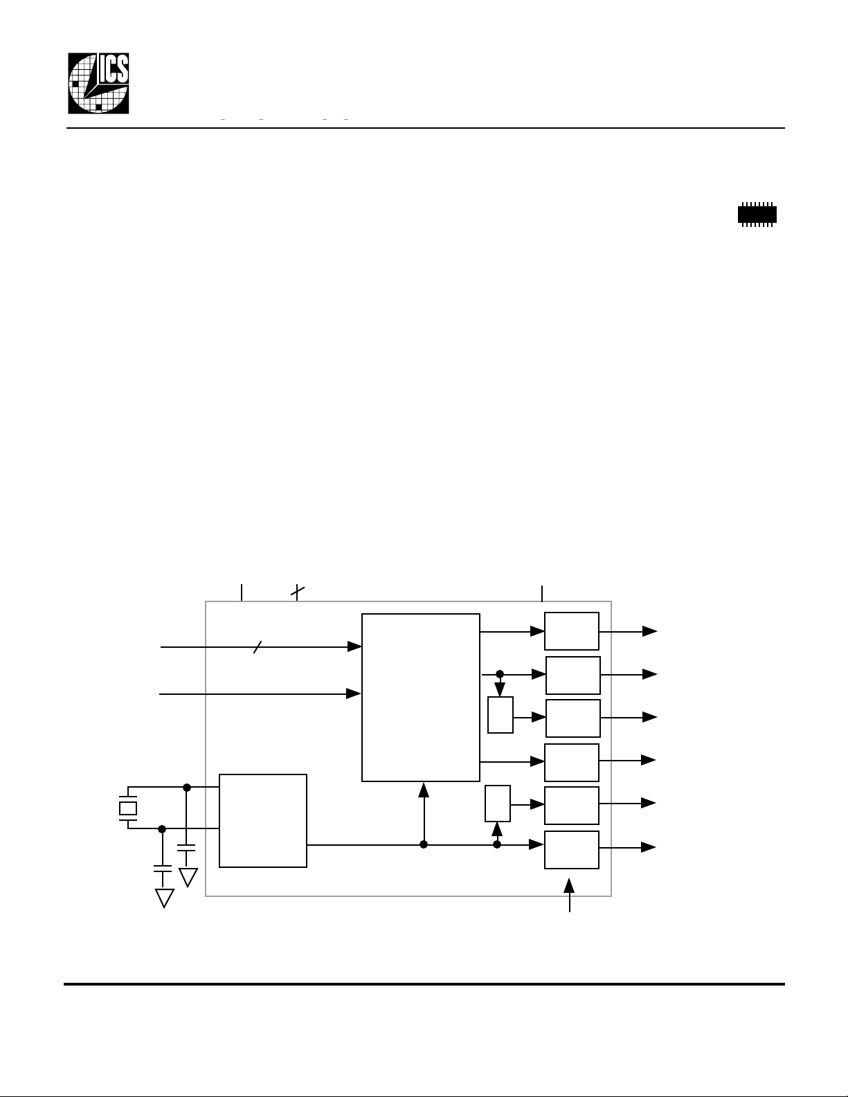
Block Diagram
ASEL1:0
DSEL
27 MHz crystal
X1
X2
VDD GND
2
Crystal
Oscillator
VDDIO
2
Clock Synthesis
and Control
Circuitry
Output
Buffer
Output
Buffer
÷2
÷2
Output
Buffer
Output
Buffer
Output
Buffer
Output
Buffer
Output Enable (all outputs)
ACLK
28.636 MHz or
35.4689 MHz
14.318 MHz or
17.7344 MHz
48 MHz
13.5 MHz
27 MHz
MDS 614-01 B 1 Revision 020199 Printed 11/14/00
Integrated Circuit Systems • 525 Race Street • San Jose •CA•95126• (408) 295-9800tel • (408) 295-9818fax
Page 2

PRELIMINARY INFORMATION
ICS614-01
Pin Assignment
OE
X1/ICLK
VDD
GND
DSEL
27M
DCLK/2
X2
1
2
3
4
5
6
7
8
ICS614-01
ICRO
16
15
14
13
12
11
10
9
C
LOCK
ASEL1
ASEL0
13.5M
VDDIO
GND
ACLK
DCLK
48MHz
16 pin Intel Graphics Clock Source
ACLK Select Table for Audio and Square Pixel
ASEL1 ASEL0 ACLK
0 0 Off
0 1 29.4923 MHz
1 0 24.5454 MHz
1 1 24.576 MHz
DCLK Select Table for NTSC/PAL
DSEL DCLK DCLK/2
0 35.4689 17.73445
1 28.63636 14.31818
All Clock frequencies are in MHz.
0=connect directly to ground
1=connect directly to VDDIO
Pin Descriptions
Number Name Type Description
1 OE I Output Enable. Tri-states all output clocks when low. All running when high (VDDIO).
2 X2 XO Crystal connection. Connect to a 27 MHz fundamental parallel mode crystal.
3 X1/ICLK XI Crystal connection. Connect to a 27 MHz fundamental parallel mode crystal, or clock
4 VDD P Connect to +5V.
5 GND P Connect to ground.
6 DSEL I Input select. Determines DCLK and DCLK/2 per table above. Must be ≤ VDDIO.
7 27M O Buffered crystal oscillator 27 MHz clock output. Amplitude = VDDIO.
8 DCLK/2 O NTSC or PAL 4X subcarrier frequency per table above. Amplitude = VDDIO.
9 48M O 48.00 MHz clock output for Intel graphics processor. Amplitude = VDDIO.
10 DCLK O NTSC or PAL 8X subcarrier frequency per table above. Amplitude = VDDIO.
11 ACLK O Audio clock, or Square Pixel clock, per table above. Amplitude = VDDIO.
12 GND P Connect to ground.
13 VDDIO P Connect to +5V or +3.3V. Amplitude of output clocks will match this voltage.
14 13.5M O Buffered crystal oscillator divided by two 13.5 MHz clock output. Amplitude = VDDIO.
15 ASEL0 I Input select 0 for ACLK. Determines ACLK frequency per table above. Must be ≤ VDDIO.
16 ASEL1 I Input select 1 for ACLK. Determines ACLK frequency per table above. Must be ≤ VDDIO.
Key: I = Input; O = output; P = power supply connection; XI, XO = crystal connections.
MDS 614-01 B 2 Revision 020199 Printed 11/14/00
Integrated Circuit Systems • 525 Race Street • San Jose •CA•95126• (408) 295-9800tel • (408) 295-9818fax
Page 3

PRELIMINARY INFORMATION
ABSOLUTE MAXIMUM RATINGS (note 1)
DC CHARACTERISTICS (VDD = 5.0V unless noted)
AC CHARACTERISTICS (VDD = 5.0V unless noted)
exposure to levels above the operating limits but below the Absolute Maximums may affect device reliability.
ICS614-01
ICRO
C
LOCK
16 pin Intel Graphics Clock Source
Electrical Specifications
Parameter Conditions Minimum Typical Maximum Units
Supply voltage, VDD Referenced to GND 7 V
Inputs and Clock Outputs Referenced to GND -0.5 VDD+0.5 V
Ambient Operating Temperature 0 70 C
Soldering Temperature Max of 10 seconds 260 C
Storage temperature -65 150 C
Operating Voltage, VDD 4.50 5.50 V
Operating Voltage, VDDIO 3.13 VDD V
Input High Voltage, VIH, X1 pin only 3.5 2.5 V
Input Low Voltage, VIL, X1 pin only 2.5 1.5 V
Input High Voltage, VIH 2 V
Input Low Voltage, VIL 0.8 V
Output High Voltage, VOH IOH=-25mA 2.4 V
Output Low Voltage, VOL IOL=25mA 0.4 V
Output High Voltage, VOH, CMOS level IOH=-8mA VDD-0.4 V
Operating Supply Current, IDD No Load 35 mA
Short Circuit Current Each output ±100 mA
Input Capacitance OE, select pins 5 pF
VIN, VCXO control voltage 0 3 V
Input Frequency 27.000000 MHz
Input Crystal Accuracy 30 ppm
Output Clock Accuracy (all but PAL square pixel) Given exact input 0 1 ppm
Output Clock Rise Time 0.8 to 2.0V, no load 1.5 ns
Output Clock Fall Time 0.8 to 2.0V, no load 1.5 ns
Output Clock Duty Cycle At VDD/2 40 60 %
Maximum Absolute Jitter, short term ±150 ps
Maximum Jitter, one sigma 50 ps
Notes: 1. Stresses beyond those listed under Absolute Maximum Ratings could cause permanent damage to the device. Prolonged
MDS 614-01 B 3 Revision 020199 Printed 11/14/00
Integrated Circuit Systems • 525 Race Street • San Jose •CA•95126• (408) 295-9800tel • (408) 295-9818fax
Page 4

PRELIMINARY INFORMATION
Inches
Millimeters
ICS614-01
ICRO
C
LOCK
16 pin Intel Graphics Clock Source
External Components/Crystal Selection
The ICS614-01 requires a minimum number of external components for proper operation. Decoupling
capacitors of 0.01 µF should be connected between VDD and GND, one between pins 4 and 5, and one
between pins 13 and 12, as close to the part as possible. A series termination resistor of 33 Ω may be used
for each clock output. The 27.000 MHz crystal must be connected as close to the chip as possible. The
crystal should be a fundamental mode, parallel resonant, 30 ppm or better. Do not use third overtone.
Crystal capacitors should be connected from pins X1 to ground and X2 to ground. In general, the value of
these capacitors is given by the following equation, where CL is the crystal load capacitance: Crystal caps
(pF) = (CL-6) x 2. So for a crystal with 16 pF load capacitance, two 20 pF caps can be used. For any given
board layout, ICS can measure the board capacitance and recommend the exact capacitance value to use.
Package Outline and Package Dimensions
E H
h x 45°
16 pin SOIC narrow
Symbol Min Max Min Max
A 0.055 0.070 1.397 1.778
b 0.013 0.019 0.330 0.483
c 0.007 0.010 0.191 0.254
D 0.385 0.400 9.779 10.160
E 0.150 0.160 3.810 4.064
H 0.225 0.245 5.715 6.223
e
h 0.016 0.406
Q 0.004 0.01 0.102 0.254
D
Q
c
e
b
A
Ordering Information
Part/Order Number Marking Shipping packaging Package Temperature
ICS614M-01 ICS614M-01 tubes 16 pin narrow SOIC 0 to 70 C
ICS614M-01T ICS614M-01 tape and reel 16 pin narrow SOIC 0 to 70 C
Rev. 12308, version A . First publication, Preliminary.
Rev. 2019, version B. Added jitter, IDD specifications, showed VDDIO on pin 13, added i752 designation.
While the information presented herein has been checked for both accuracy and reliability, Integrated Circuit Systems, Incorporated (ICS) assumes no responsibility for either its
use or for the infringement of any patents or other rights of third parties, which would result from its use. No other circuits, patents, or licenses are implied. This product is
intended for use in normal commercial applications. Any other applications such as those requiring extended temperature range, high reliability, or other extraordinary
environmental requirements are not recommended without additional processing by ICS. ICS reserves the right to change any circuitry or specifications without notice. ICS does
not authorize or warrant any ICS product for use in life support devices or critical medical instruments.
MDS 614-01 B 4 Revision 020199 Printed 11/14/00
Integrated Circuit Systems • 525 Race Street • San Jose •CA•95126• (408) 295-9800tel • (408) 295-9818fax
 Loading...