

Page 1
ICS601-01
Low Phase Noise Clock Multiplier
Description
The ICS601-01 is a low cost, low phase noise, high
performance clock synthesizer for any applications
that require low phase noise and low jitter. It is
ICS’ lowest phase noise multiplier, and also the
lowest CMOS part in the industry. Using ICS’
patented analog and digital Phase Locked Loop
(PLL) techniques, the chip accepts a 10-27 MHz
crystal or clock input, and produces output clocks
up to 156 MHz at 3.3 V.
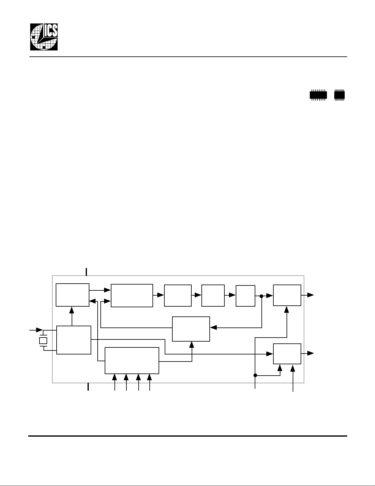
Block Diagram
Features
• Packaged in 16 pin SOIC or TSSOP
• Uses fundamental 10 - 27 MHz crystal, or clock
• Patented PLL with the lowest phase noise
• Output clocks up to 156 MHz at 3.3 V
• Low phase noise: -132 dBc/Hz at 10 kHz
• Output Enable function tri states outputs
• Low jitter - 18 ps one sigma
• Full swing CMOS outputs with 25 mA drive
capability at TTL levels
• Advanced, low power, sub-micron CMOS process
• Industrial temperature version available
• 3.3 V or 5 V operation
X1/ICLK
X2
VDD
Reference
Divide
Crystal
Oscillator
GND
Phase
Comparator
ROM Based
Multipliers
S3 S2
Charge
Pump
VCO
Divide
S0S1
Loop
Filter
VCO
OE
Output
Buffer
Output
Buffer
REFEN
CLK
REFOUT
MDS 601-01 G 1 Revision 090800 Printed 11/14/00
Integrated Circuit Systems, Inc. • 525 Race Street • San Jose •CA•95126• (408) 295-9800tel • www.icst.com
Page 2
ICS601-01
Low Phase Noise Clock Multiplier
Pin Assignment
CLK
REFEN
VDD
VDD
VDD
X1/ICLK
X2
S1
1
2
3
4
5
6
7
8
ICS601-01
Pin Descriptions
16
15
14
13
12
11
10
9
GND
GND
GND
REFOUT
OE
S0
S3
S2
Multiplier Select Table
S3 S2 S1 S0 CLK (see note 2 on following page)
0 0 0 0 TEST
0 0 0 1 TEST
0 0 1 0 Input x1
0 0 1 1 Input x3
0 1 0 0 Input x4
0 1 0 1 Input x5
0 1 1 0 Input x6
0 1 1 1 Input x8
1 0 0 0 TEST
1 0 0 1 Crystal osc. pass through (no PLL)
1 0 1 0 Input x2
1 0 1 1 TEST
1 1 0 0 Input x8
1 1 0 1 Input x10
1 1 1 0 Input x12
1 1 1 1 Input x16
0=connect directly to ground
1=connect directly to VDD
Number Name Type Description
1 CLK O Clock output from VCO. Output frequency equals the input frequency times multiplier.
2 REFEN I Reference clock enable. Turns off the buffered crystal oscillator clock (stops low) when low.
3 VDD P Connect to +3.3V or +5V. Must match other VDDs.
4 VDD P Connect to +3.3V or +5V. Must match other VDDs.
5 VDD P Connect to +3.3V or +5V. Must match other VDDs.
6 X2 XO Crystal connection. Connect to a 10 - 27 MHz fundamental parallel mode crystal.
7 S1 I Multiplier select pin 1. Determines CLK output per table above. Internal pull-up.
8 X1/ICLK XI Crystal connection. Connect to a 10-27 MHz fundamental parallel mode crystal, or clock
9 S2 I Multiplier select pin 2. Determines CLK output per table above. Internal pull-up.
10 S3 I Multiplier select pin 3. Determines CLK output per table above. Internal pull-up.
11 S0 I Multiplier select pin 0. Determines CLK output per table above. Internal pull-up.
12 OE I Output Enable. Tri-states both output clocks when low. Internal pull-up.
13 REFOUT O Buffered crystal oscillator clock output. Controlled by REFEN.
14 GND P Connect to ground.
15 GND P Connect to ground.
16 GND P Connect to ground.
Key: I = Input with internal pull-up resistor; O = output; P = power supply connection; XI, XO = crystal
connections.
MDS 601-01 G 2 Revision 090800 Printed 11/14/00
Integrated Circuit Systems, Inc. • 525 Race Street • San Jose •CA•95126• (408) 295-9800tel • www.icst.com
Page 3

ICS601-01
Low Phase Noise Clock Multiplier
Achieving Low Phase Noise
Figure 1 shows a typical phase noise measurement in a 125 MHz system. There are a few simple steps that
can be taken to achieve these levels of phase noise from the ICS601-01. Variations in VDD will increase the
phase noise, so it is important to have a stable, low noise supply voltage at the device. Use decoupling
capacitors of 0.1 µF in parallel with 0.01 µF. It is important to have these capacitors as close as possible to
the ICS601-01 supply pins.
Disabling the REFOUT clock is also important for achieving low phase noise; lab tests have shown that this
can reduce the phase noise by as much as 10 dBc/Hz.
0
-20
-40
-60
-80
Phase Noise (dBc/Hz)
-100
-120
-140
10.0E+0 100.0E+0 1.0E+3 10.0E+3 100.0E+3 1.0E+6 10.0E+6
Offset from Carrier (Hz)
Figure 1. Phase Noise of ICS601-01 at 125 MHz out, 25 MHz crystal input.
VDD = 3.3 V, REFOUT disabled.
External Components/Crystal Selection
The ICS601-01 requires a minimum number of external components for proper operation. Decoupling
capacitors of 0.01 µF and 0.1 µF should be connected between VDD and GND, as close to the part as
possible. A series termination resistor of 33 Ω may be used for each clock output. The crystal must be
connected as close to the chip as possible. The crystal should be fundamental mode, parallel resonant. Do
not use third overtone. For exact tuning when using a crystal, capacitors should be connected from pins X1
to ground and X2 to ground. In general, the value of these capacitors is given by the following equation,
where CL is the crystal load capacitance: Crystal caps (pF) = (CL-5) x 2. So for a crystal with 16 pF load
capacitance, two 22 pF caps can be used. For any given board layout, ICS can measure the board
capacitance and recommend the exact capacitance value to use.
MDS 601-01 G 3 Revision 090800 Printed 11/14/00
Integrated Circuit Systems, Inc. • 525 Race Street • San Jose •CA•95126• (408) 295-9800tel • www.icst.com
Page 4

ICS601-01
ABSOLUTE MAXIMUM RATINGS (note 1)
DC CHARACTERISTICS (VDD = 3.3 V unless noted)
AC CHARACTERISTICS (VDD = 3.3 V unless noted)
exposure to levels above the operating limits but below the Absolute Maximums may affect device reliability.
2. The phase relationship between input and output can change at power up. For a fixed phase relationship, see the ICS570
or ICS670.
3. Switching occurs nominally at VDD/2.
Low Phase Noise Clock Multiplier
Electrical Specifications
Parameter Conditions Minimum Typical Maximum Units
Supply voltage, VDD Referenced to GND 7 V
Inputs and Clock Outputs Referenced to GND -0.5 VDD+0.5 V
Ambient Operating Temperature 0 70 °C
Ambient Operating Temperature, I version Industrial temperature -40 85 °C
Soldering Temperature Max of 10 seconds 260 °C
Storage temperature -65 150 °C
Operating Voltage, VDD 3.0 5.5 V
Input High Voltage, VIH, X1/ICLK pin only Note 3 (VDD/2)+1 V
Input Low Voltage, VIL, X1/ICLK pin only Note 3 (VDD/2)-1 V
Input High Voltage, VIH 2 V
Input Low Voltage, VIL 0.8 V
Output High Voltage, VOH, CMOS level IOH=-4mA VDD-0.4 V
Output High Voltage, VOH IOH=-12mA 2.4 V
Output Low Voltage, VOL IOL=12mA 0.4 V
Operating Supply Current, IDD No Load, 125 MHz 22 30 mA
Short Circuit Current Each output ±40 ±60 mA
Input Capacitance OE, select pins 5 pF
Input Frequency 10 27 MHz
Output Frequency at 3.3V or 5V 156 MHz
Output Clock Rise Time 0.8 to 2.0V, no load 1.5 ns
Output Clock Fall Time 0.8 to 2.0V, no load 1.5 ns
Output Clock Duty Cycle At VDD/2 45 50 55 %
Maximum Absolute Jitter, short term, 125 MHz No load, REF off ±50 ±75 ps
Maximum Jitter, one sigma, 125 MHz (x5) No load, REF off 18 25 ps
Phase Noise, relative to carrier, 125 MHz (x5) 100 Hz offset -105 -108 dBc/Hz
Phase Noise, relative to carrier, 125 MHz (x5) 1 kHz offset -120 -123 dBc/Hz
Phase Noise, relative to carrier, 125 MHz (x5) 10 kHz offset -128 -132 dBc/Hz
Phase Noise, relative to carrier, 125 MHz (x5) 100 kHz offset -121 -125 dBc/Hz
Notes: 1. Stresses beyond those listed under Absolute Maximum Ratings could cause permanent damage to the device. Prolonged
MDS 601-01 G 4 Revision 090800 Printed 11/14/00
Integrated Circuit Systems, Inc. • 525 Race Street • San Jose •CA•95126• (408) 295-9800tel • www.icst.com
Page 5

Low Phase Noise Clock Multiplier
SOIC
TSSOP
Package Outline and Package Dimensions
(For current dimensional specifications, see JEDEC no. 95.)
E H
ICS601-01
16 pin narrow SOIC, TSSOP (in mm)
Symbol Min Max Min Max
A 1.35 1.75 - 1.20
A1 0.10 0.25 0.05 0.15
B 0.33 0.51 0.19 0.30
C 0.19 0.25 0.09 0.20
D 9.80 10.00 4.90 5.10
E 3.80 4.00 4.30 4.50
H 5.80 6.20
e
L 0.40 1.27 0.45 0.75
D
A
A1
e
B
C
L
Ordering Information
Part/Order Number Marking Shipping packaging Package Temperature
ICS601M-01 ICS601M-01 tubes 16 pin narrow SOIC 0 to 70 °C
ICS601M-01T ICS601M-01 tape and reel 16 pin narrow SOIC 0 to 70 °C
ICS601M-01I ICS601M-01I tubes 16 pin narrow SOIC -40 to 85 °C
ICS601M-01IT ICS601M-01I tape and reel 16 pin narrow SOIC -40 to 85 °C
ICS601G-01 ICS601G-01 tubes 16 pin TSSOP 0 to 70 °C
ICS601G-01T ICS601G-01 tape and reel 16 pin TSSOP 0 to 70 °C
While the information presented herein has been checked for both accuracy and reliability, Integrated Circuit Systems, Incorporated (ICS) assumes no responsibility for either its
use or for the infringement of any patents or other rights of third parties, which would result from its use. No other circuits, patents, or licenses are implied. This product is
intended for use in normal commercial applications. Any other applications such as those requiring extended temperature range, high reliability, or other extraordinary
environmental requirements are not recommended without additional processing by ICS. ICS reserves the right to change any circuitry or specifications without notice. ICS does
not authorize or warrant any ICS product for use in life support devices or critical medical instruments.
MDS 601-01 G 5 Revision 090800 Printed 11/14/00
Integrated Circuit Systems, Inc. • 525 Race Street • San Jose •CA•95126• (408) 295-9800tel • www.icst.com
 Loading...