

Page 1
ICS580-01
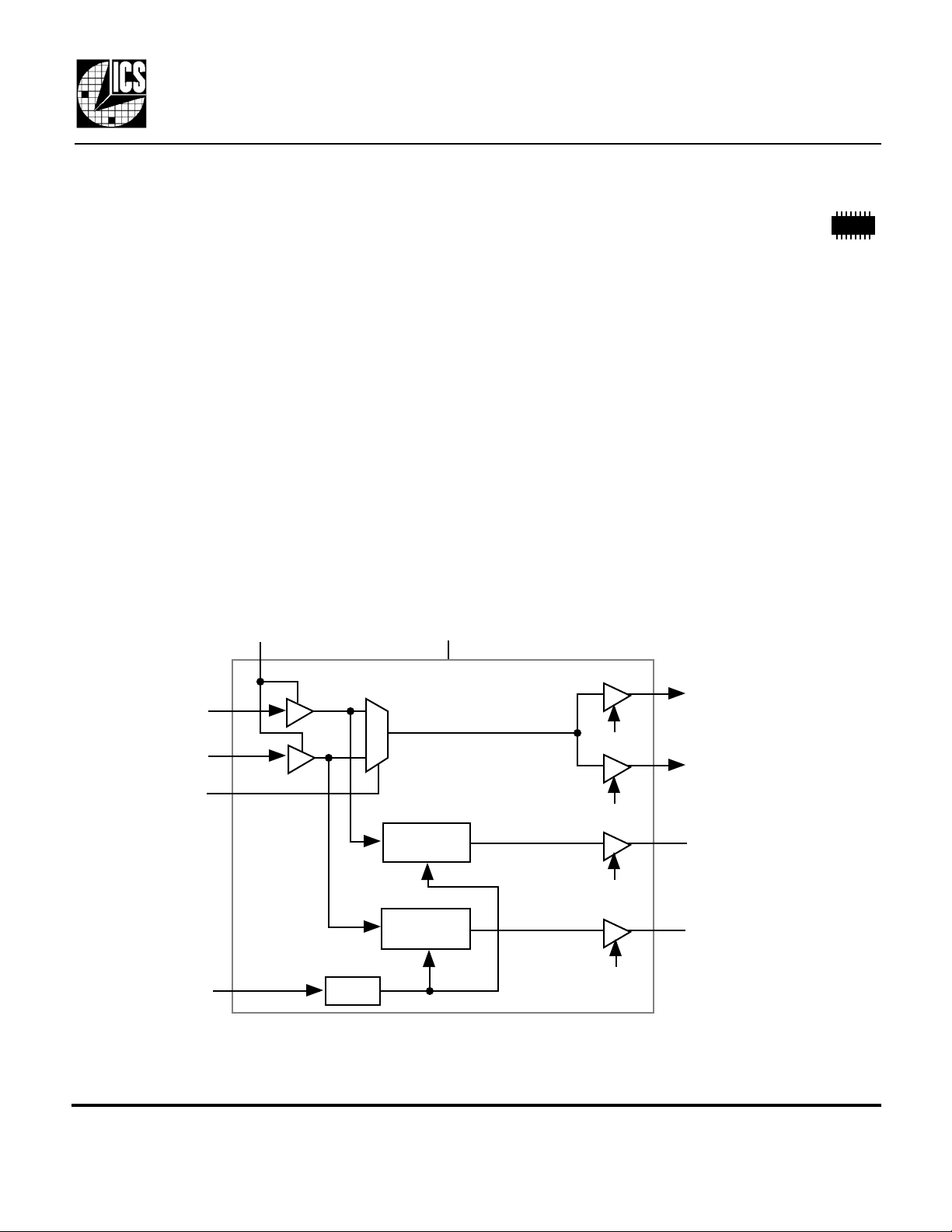
Glitch-Free Clock Multiplexer
Description
The ICS580-01 is a clock multiplexer (mux)
designed to switch between 2 clock sources with no
glitches or short pulses. The operation of the mux is
controlled by an input pin but the part can also be
configured to switch automatically if one of the
input clocks stops. The part also provides clock
detection by reporting when an input clock has
stopped.
For a clock mux with zero delay and smooth
switching, see either the ICS581-01 or ICS581-02.
Block Diagram
VDDI
VDDC
Features
• Packaged in 16 pin narrow (150 mil) SOIC
• No short pulses or glitches on output
• Operates to 200 MHz
• Does not add jitter or phase noise to the clock
• User controlled or automatic switching
• Low skew outputs
• Clock detect feature
• Ideal for systems with backup or redundant clocks
• Selectable timeouts for clock detection
• Separate supply voltages allow power supply voltage
translation
• Operates to 2.5 V
CLK1
INB
INA
SELB
DIV
MDS 580-01 A 1 Revision 030300 Printed 11/28/00
Timer
1
0
Transition
Detector
Transition
Detector
OE1
CLK2
OE2
NO_INA
OE3
NO_INB
OE4
Integrated Circuit Systems, Inc. • 525 Race Street • San Jose •CA•95126• (408) 295-9800tel • www.icst.com
Page 2
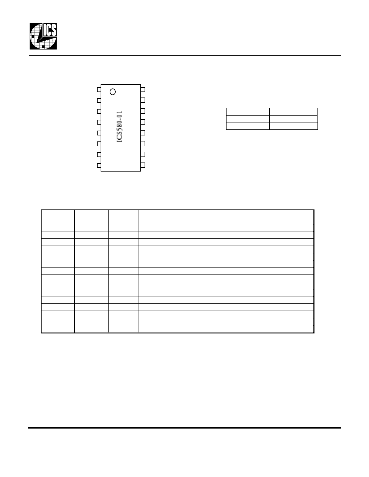
Pin Assignment
ICS580-01
Glitch-Free Clock Multiplexer
SELB
DIV
VDDI
INA
INB
GND
OE4
OE3
1
16
2
3
4
5
6
7
8
1415CLK1
13
12
11
10
9
Pin Descriptions
Number Name Type Description
1 SELB I Mux select. Selects INB when high. Internal pull-up.
2 DIV I Time out select. See table above. Internal pull-up.
3 VDDI P Supply for input clocks only. Can be higher than VDDC.
4 INA I Input Clock A.
5 INB I Input Clock B.
6 GND P Connect to ground.
7 OE4 I Output Enable. Tri-states NO_INB when low. Internal pull-up.
8 OE3 I Output Enable Tri-states NO_INA when low. Internal pull-up.
9 OE2 I Output enable. Tri-states CLK2 when low. Internal pull-up.
10 GND P Connect to ground.
11 NO_INB O Goes high when clock on INB stops.
12 NO_INA O Goes high when clock on INA stops.
13 CLK2 O Clock 2 Output. Low skew compared to CLK1.
14 CLK1 O Clock 1 Output. Low skew compared to CLK2.
15 VDDC P Main chip supply. Output clocks amplitude will match this VDD.
16 OE1 I Output Enable. Tri-states CLK1 when low. Internal pull-up.
OE1
VDDC
CLK2
NO_INA
NO_INB
GND
OE2
Timeout Selection
DIV Nominal Timeout
0 600 ns
1 75 ns
Key: I = Input; O = output; P = power supply connection
MDS 580-01 A 2 Revision 030300 Printed 11/28/00
Integrated Circuit Systems, Inc. • 525 Race Street • San Jose •CA•95126• (408) 295-9800tel • www.icst.com
Page 3

ICS580-01
Glitch-Free Clock Multiplexer
Device Operation and Applications
The ICS580-01 consists of a glitch free mux between INA and INB controlled by SELB. The device is
designed to switch between 2 clocks, whether running or not. In the first example, clocks are running on
both INA and INB. When SELB changes, the output clock goes low after 3 cycles of the output clock
(nominally). The output then stays low for 3 cycles of the new input clock (nominally) and then starts with
the new input clock. This is shown in Figure 1.
Figure 1
INA
INB
SELB
CLK1, 2
In the second example, one of the inputs was selected and running but has since stopped (either high or low).
This is indicated by either NO_INA or NO_INB going high depending on whether INA or INB has
stopped. These signals go high following a selectable time-out period after the clock has stopped. The
timeout period is determined by the DIV input pin. The SELB pin is now changed to select the new input
clock which is running. The output clock immediately goes low and stays low for 3 cycles of the new input
clock and then starts with the new input clock. Figure 2 shows an example of this.
Figure 2
INA
INB
SELB
Timeout
NO_INA
CLK1, 2
MDS 580-01 A 3 Revision 030300 Printed 11/28/00
Integrated Circuit Systems, Inc. • 525 Race Street • San Jose •CA•95126• (408) 295-9800tel • www.icst.com
Page 4

ICS580-01
Glitch-Free Clock Multiplexer
In the third example, the ICS580-01 is configured to automatically switch clocks when an an input stops.
The clock that could stop is connected to INA while the backup, always running, clock is connected to INB.
The output NO_INA is connected to SELB. This means that when the clock on INA stops, NO_INA
goes high selecting the clock on INB which is muxed to the output after 3 cycles. When the clock on
INA restarts, NO_INA immediately goes low, selecting the clock on INA. The output then switches in
the manner described in the first example.
The circuit diagram in Figure 3 shows a typical connection for this example. Note that CLK2 and
NO_INB are unused and so are disabled by grounding OE2 and OE4. A 33Ω series termination resistor
is used on the clock output and 2 decoupling capacitors of 0.01µF are used. All other inputs are left
floating and are therefore pulled high by the on-chip pull-ups.
Figure 3
VDD
Normal
Clock
Backup
Clock
SELB
DIV
VDDI
0.01µF 33Ω
INA
INB
GND
OE4
OE3
OE1
VDDC
CLK1
CLK2
NO_INA
NO_INB
GND
OE2
0.01µF
Output
Clock
Output Enable
Each output has a dedicated output enable pin. If an output is unused, it should be tri-stated by tying the
appropriate output enable pin to ground.
External Components
The ICS580-01 requires two 0.01µF decoupling capacitors, one between VDDI and GND and one between
VDDC and GND. Series termination resistors of 33Ω can be used on CLK1 and CLK2.
Split Power Supplies
The VDDI pin provides the power for the INA and INB input buffers only. All the other inputs and the
rest of the chip are connected to VDDC. This allows for supply voltage translation. For example, INA and
INB could be 5 V clocks (VDDI=5 V) and the rest of the chip could use a 3.3 V supply on VDDC giving
3.3 V output clocks. For correct operation VDDI must always be greater than or equal to VDDC.
MDS 580-01 A 4 Revision 030300 Printed 11/28/00
Integrated Circuit Systems, Inc. • 525 Race Street • San Jose •CA•95126• (408) 295-9800tel • www.icst.com
Page 5

ICS580-01
DC CHARACTERISTICS (VDDC = VDDI = 3.3 V unless noted)
AC CHARACTERISTICS (VDDC = VDDI = 3.3 V unless noted)
Glitch-Free Clock Multiplexer
Electrical Specifications
Parameter Conditions Minimum Typical Maximum Units
ABSOLUTE MAXIMUM RATINGS
Supply voltage, VDD Referenced to GND 7 V
Inputs and Clock Outputs Referenced to GND -0.5 VDD+0.5 V
Ambient Operating Temperature 0 70 °C
Ambient Operating Temperature, I version Industrial temperature -40 85 °C
Soldering Temperature Max of 10 seconds 260 °C
Storage temperature -65 150 °C
Operating Voltage, VDDC 2.5 5.5 V
Operating Voltage, VDDI VDDC 5.5 V
Input High Voltage, VIH, note 3 INA and INB only (VDDC/2)+1 VDDC/2 VDDI V
Input Low Voltage, VIL, note 3 INA and INB only VDDC/2 (VDDC/2)-1 V
Input High Voltage, VIH Non-clock inputs 2 VDDC V
Input Low Voltage, VIL Non-clock inputs 0.8 V
Output High Voltage, VOH IOH=-12mA VDDC-0.5 V
Output Low Voltage, VOL IOL=12mA 0.5 V
Operating Supply Current, IDD 50 MHz inputs, no load 6 mA
Short Circuit Current ±70 mA
On-chip pull-up resistor, non-clock inputs Pull-up to VDDC 250 kΩ
Input Capacitance 4 pF
Input Frequency, INA and INB. Note 1. VDDC = 5 V 1/timeout 270 MHz
VDDC = 3.3 V 1/timeout 220 MHz
VDDC = 2.7 V 1/timeout 180 MHz
Propagation Delay, INA or INB to output VDDC = 5 V 4 8 ns
VDDC = 3.3 V 5 10 ns
VDDC = 2.7 V 6 12 ns
Transition Detector Timeout, DIV=0 VDDI = 5 V 175 350 700 ns
VDDI = 3.3 V 500 1000 2000 ns
VDDI = 2.7 V 750 1500 3000 ns
Transition Detector Timeout, DIV=1 VDDI = 5 V 20 40 80 ns
VDDI = 3.3 V 55 110 210 ns
VDDI = 2.7 V 100 200 400 ns
Output Clock Rise Time 1.5 ns
Output Clock Fall Time 1.5 ns
Output Clock Skew, CLK1 to CLK2 Note 2 -250 0 250 ps
Note 1. Frequencies less than the minimum may cause a timeout, which will not guarantee glitch-free switching unless the clock is
actually stopped.
Note 2. Assumes identically loaded outputs with identical rise times, measured at VDD/2.
Note 3. Output duty cycle is set by duty cycle of input clock at VDDC/2.
MDS 580-01 A 5 Revision 030300 Printed 11/28/00
Integrated Circuit Systems, Inc. • 525 Race Street • San Jose •CA•95126• (408) 295-9800tel • www.icst.com
Page 6

Glitch-Free Clock Multiplexer
Inches
Millimeters
Package Outline and Package Dimensions
(For current dimensional specifications, see JEDEC publication no. 95.)
16 pin SOIC narrow
Symbol Min Max Min Max
E H
D
ICS580-01
A 0.059 0.069 1.50 1.75
A1 0.004 0.0098 0.10 0.25
B 0.013 0.020 0.33 0.51
C 0.007 0.0098 0.19 0.25
D 0.386 0.394 9.80 10.00
E 0.150 0.157 3.80 4.00
e
H 0.228 0.244 5.80 6.20
L 0.016 0.05 0.41 1.27
A1
C
e
B
L
A
Ordering Information
Part/Order Number Marking Package Temperature
ICS580M-01 ICS580M-01 16 pin SOIC 0 to 70 °C
ICS580M-01T ICS580M-01 16 pin SOIC on tape and reel 0 to 70 °C
ICS580M-01I ICS580M-01I 16 pin SOIC -40 to 85°C
ICS580M-01IT ICS580M-01I 16 pin SOIC on tape and reel -40 to 85°C
While the information presented herein has been checked for both accuracy and reliability, Integrated Circuit Systems, Incorporated (ICS) assumes no responsibility for either its
use or for the infringement of any patents or other rights of third parties, which would result from its use. No other circuits, patents, or licenses are implied. This product is
intended for use in normal commercial applications. Any other applications such as those requiring extended temperature range, high reliability, or other extraordinary
environmental requirements are not recommended without additional processing by ICS. ICS reserves the right to change any circuitry or specifications without notice. ICS does
not authorize or warrant any ICS product for use in life support devices or critical medical instruments.
MDS 580-01 A 6 Revision 030300 Printed 11/28/00
Integrated Circuit Systems, Inc. • 525 Race Street • San Jose •CA•95126• (408) 295-9800tel • www.icst.com
 Loading...