

Page 1
ICS552-01A
Crystal Oscillator & Multiplier with 8 Low Skew Outputs
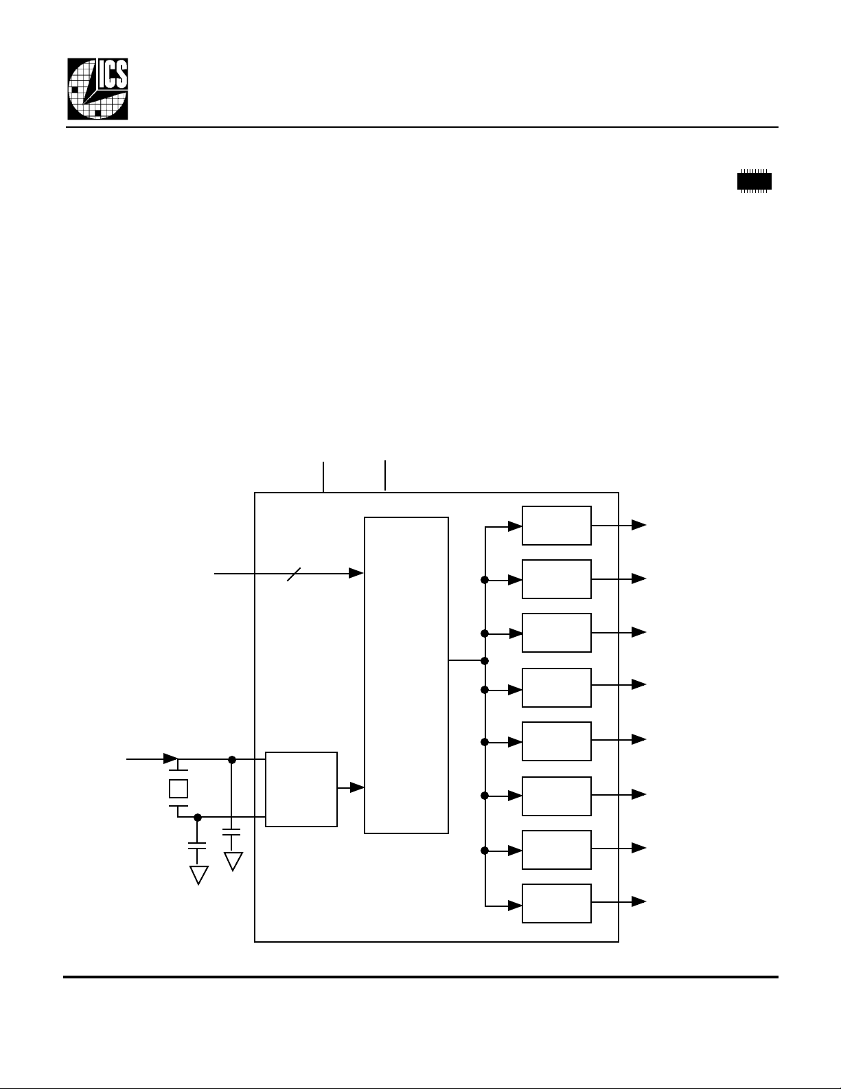
Description
The ICS552-01A produces 8 low skew
copies of a multiple of the input when a
clock or fundamental, parallel-mode crystal
is connected to it. Unlike other clock
drivers, it does not require a separate
oscillator for the input. Using a phaselocked loop (PLL) to multiply the input
frequency, it is ideal for generating and
distributing multiple high frequency clocks.
Block Diagram
VDD GND
Features
• Packaged in 20 pin SSOP (QSOP)
• Input frequency of 10.0 - 27.0 MHz
• Contains on-chip multiplier with selections
of x1, x1.33, x2, x2.66, x3, x3.33, x4,
x4.66, x5, and x6
• Provides 8 low skew outputs (<250 ps)
• Output clock duty cycle of 40/60 at 3.3 V
• Operating voltages of 3.0 V to 5.5 V
• Industrial temperature available
• Power Down and Tri state modes
Output
Buffer
CLK1
10.0 - 27.0 MHz
crystal or clock
S3:S0
X1
X2
4
Clock
Buffer/
Crystal
Oscillator
PLL
Multiplier
Output
Buffer
Output
Buffer
Output
Buffer
Output
Buffer
Output
Buffer
Output
Buffer
Output
Buffer
CLK2
CLK3
CLK4
CLK5
CLK6
CLK7
CLK8
MDS 552-01 AB 1 Revision 032200 Printed 11/14/00
Integrated Circuit Systems • 525 Race Street • San Jose • CA • 95126 • (408) 295-9800tel • www.icst.com
Page 2
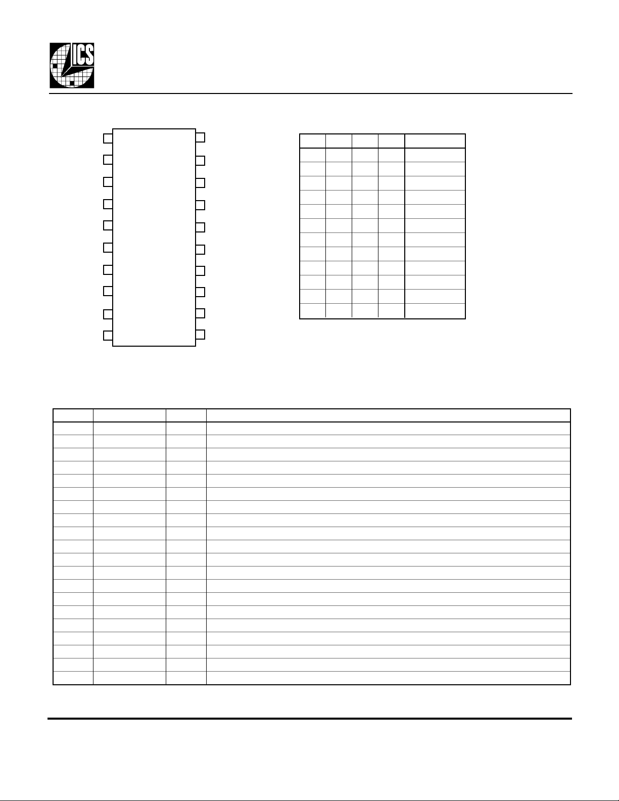
Pin Assignment
S2
1
2
3
4
5
6
7
8
9
10
DC
X2
X1/ICLK
VDD
GND
CLK1
CLK2
CLK3
CLK4
20 pin SSOP (QSOP)
ICS552-01A
Crystal Oscillator & Multiplier with 8 Low Skew Outputs
Multiplier Select Table
S0
20
19
18
17
16
15
14
13
12
11
DC
CLK8
CLK7
VDD
S3
GND
CLK6
CLK5
S1
S3 S2 S1 S0 Multiplier
0 0 0 0 Power Down
0 0 0 1 x1
0 0 1 0 x1.333
0 0 1 1 x2
0 1 0 0 x2.666
0 1 0 1 x3
0 1 1 0 x3.333
0 1 1 1 x4
1 0 0 0 x5
1 0 0 1 x4.66
1 0 1 0 x6
1 1 0 1 Tri state All
0 = connect directly to ground.
1 = connect directly to VDD.
All clocks stop low in Power Down state.
All clocks outputs are high impedance in 1101 mode.
Pin Descriptions
Pin # Name Type Description
1 DC - Don't connect.
2 X2 XO Crystal connection. Connect to a 10 - 27 MHz fundamental mode crystal.
3 X1/ICLK XI Crystal connection. Connect to a 10 - 27 MHz fundamental mode crystal, or clock.
4 VDD P Connect to +3.3 V or +5.0 V. Decouple with pin 6.
5 S2 I Multiplier Select Pin 2 per table above.
6 GND P Connect to ground.
7
8 CLK2 O Clock Output 2.
9 CLK3 O Clock Output 3.
10 CLK4 O Clock Output 4.
11 S1 I Multiplier Select Pin 1 per table above.
12 CLK5 O Clock Output 5.
13 CLK6 O Clock Output 6.
14 GND P Connect to ground.
15 S3 I Multiplier Select Pin 3 per table above.
16 VDD P Connect to +3.3 V or +5.0 V. Decouple with pin 14.
17 CLK7 O Clock Output 7.
18 CLK8 O Clock Output 8.
19 DC - Don't connect.
20 S0 I Multiplier Select Pin 0 per table above.
CLK1 O Clock Output 1.
Key: I = Input; O = output; P = power supply connection, XI, XO = crystal connections
MDS 552-01 AB 2 Revision 032200 Printed 11/14/00
Integrated Circuit Systems • 525 Race Street • San Jose • CA • 95126 • (408) 295-9800tel • www.icst.com
Page 3

ICS552-01A
ABSOLUTE MAXIMUM RATINGS (note 1)
DC CHARACTERISTICS (VDD = 3.3 V or 5 V unless noted)
AC CHARACTERISTICS (VDD = 3.3 V or 5 V unless noted)
exposure to levels above the operating limits but below the Absolute Maximums may affect device reliability.
Crystal Oscillator & Multiplier with 8 Low Skew Outputs
Electrical Specifications
Parameter Conditions Minimum Typical Maximum Units
Supply voltage, VDD Referenced to GND 7 V
Inputs and Clock Outputs Referenced to GND -0.5 VDD+0.5 V
Ambient Operating Temperature Commercial 0 70 °C
Industrial -40 85 °C
Soldering Temperature Max of 10 seconds 260 °C
Storage temperature -65 150 °C
Operating Voltage, VDD 3.0 5.5 V
Input High Voltage, VIH ICLK (VDD/2)+1 VDD/2 V
Input Low Voltage, VIL ICLK VDD/2 (VDD/2)-1 V
Input High Voltage, VIH S3:S0 2 V
Input Low Voltage, VIL S3:S0 0.8 V
Output High Voltage, VOH VDD=3.3V, IOH=-8mA 2.4 V
Output Low Voltage, VOL VDD=3.3V, IOL=8mA 0.4 V
Output High Voltage, VOH, VDD = 3.3 or 5 V IOH=-8mA VDD-0.4 V
Operating Supply Current, IDD, at 3.3 V No Load, 25 MHz in, x4 35 mA
Operating Supply Current, IDD, at 5 V No Load, 25 MHz in, x4 59 mA
Power Down Supply Current, IDD, at 3.3 V S3:S0 = 0 (Gnd) 55 µA
Short Circuit Current, VDD = 3.3 V Each output ±50 mA
Input Crystal or Clock Frequency 10 27 MHz
Output Clock Rise Time 0.8 to 2.0 V 1.5 ns
Output Clock Fall Time 2.0 to 0.8 V 1.5 ns
Output Clock Duty Cycle At VDD/2 40 50 60 %
Output to Output Skew Rising edges at VDD/2 250 ps
Note: 1. Stresses beyond those listed under Absolute Maximum Ratings could cause permanent damage to the device. Prolonged
External Components
A minimum number of external components are required for proper operation. A decoupling capacitor of
0.01 uF should be connected between VDD and GND on pins 4 and 6, and 16 and 14. Other VDDs and
GNDs can be connected to these pins or directly to their respective power planes. A 33 Ω series terminating
resistor may be used on the clock output if the trace is longer than 1-inch.
The crystal should be a fundamental mode (do not use third overtone), parallel resonant, with accuracy as
required by the application. Crystal capacitors should be connected from pins X1 to ground and X2 to
ground. The value of these capacitors is given by the following equation, where CL is the crystal load
capacitance: Crystal caps (pF) = (CL-12) x 2. So for a crystal with 18pF load capacitance, two 12pF caps
should be used. For a clock input, connect it to X1/ICLK, and leave X2 unconnected (floating).
MDS 552-01 AB 3 Revision 032200 Printed 11/14/00
Integrated Circuit Systems • 525 Race Street • San Jose • CA • 95126 • (408) 295-9800tel • www.icst.com
Page 4

Crystal Oscillator & Multiplier with 8 Low Skew Outputs
Inches
Millimeters
Package Outline and Package Dimensions
(For current dimensional specifications, see JEDEC Publication No. 95.)
20 pin SSOP
Symbol Min Max Min Max
A 0.053 0.069 1.35 1.75
A1 0.004 0.010 0.10 0.25
b 0.008 0.012 0.20 0.30
c 0.007 0.010 0.19 0.25
D 0.337 0.344 8.56 8.74
e
E 0.228 0.244 5.79 6.20
E1 0.150 0.157 3.81 3.99
L 0.016 0.050 0.41 1.27
INDEX
AREA
E1 E
1 2
D
ICS552-01A
A1 c
A
e
b
L
Ordering Information
Part/Order Number Marking Package Shipping Temperature
ICS552R-01 ICS552R-01 20 pin SSOP Tubes 0 to 70 °C
ICS552R-01T ICS552R-01 20 pin SSOP Tape and Reel 0 to 70 °C
ICS552R-01I ICS552R-01I 20 pin SSOP Tubes -40 to 85 °C
ICS552R-01IT ICS552R-01I 20 pin SSOP Tape and Reel -40 to 85 °C
While the information presented herein has been checked for both accuracy and reliability, Integrated Circuit Systems, Incorporated (ICS) assumes no responsibility for either its
use or for the infringement of any patents or other rights of third parties, which would result from its use. No other circuits, patents, or licenses are implied. This product is
intended for use in normal commercial applications. Any other applications such as those requiring extended temperature range, high reliability, or other extraordinary
environmental requirements are not recommended without additional processing by ICS. ICS reserves the right to change any circuitry or specifications without notice. ICS does
not authorize or warrant any ICS product for use in life support devices or critical medical instruments.
MDS 552-01 AB 4 Revision 032200 Printed 11/14/00
Integrated Circuit Systems • 525 Race Street • San Jose • CA • 95126 • (408) 295-9800tel • www.icst.com
 Loading...