

Page 1
ADVANCE INFORMATION
ICS548-03
Low Skew Clock Inverter and Divider
Description
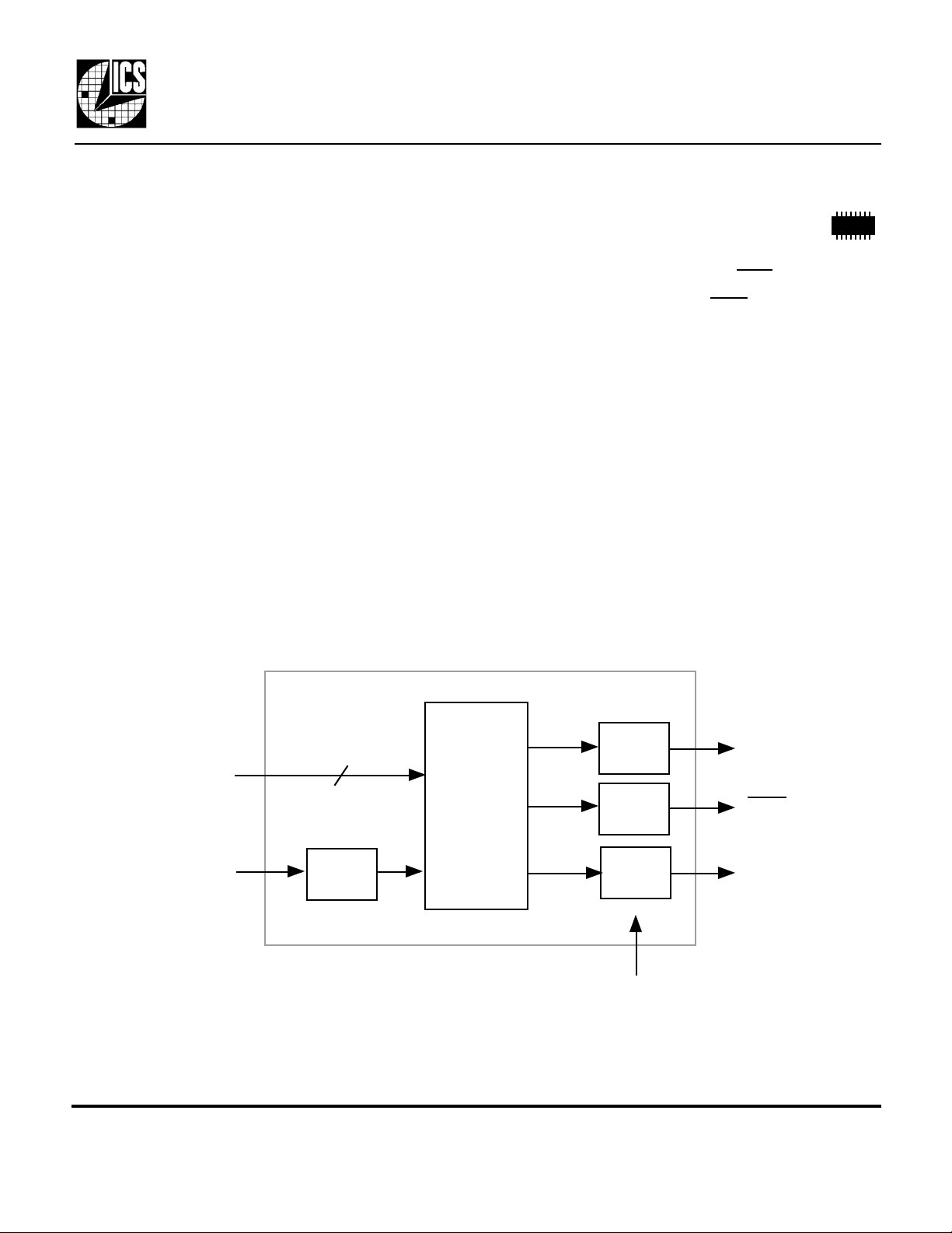
The ICS548-03 is a low cost, low skew, high
performance general-purpose clock designed to
produce a set of one output clock, one inverted
output clock, and one clock divided-by-2. Using
our patented analog Phase-Locked Loop (PLL)
techniques, the device operates from a frequency
range from 10 MHz to 120 MHz in the PLL mode,
and up to 160 MHz in the non-PLL mode.
In applications that to need maintain low phase
noise in the clock tree, the non-PLL (when
S3=S2=1) mode should be used.
This chip is not a zero delay buffer. Many
applications may be able to use the ICS527 for zero
delay dividers.
Block Diagram
Features
• Packaged in 16 pin narrow (150 mil) SOIC
• Input clock up to 160 MHz in the non-PLL mode
• Provides clock outputs of CLK, CLK, and CLK/2
• Low skew (500 ps) on CLK, CLK, and CLK/2
• All outputs can be tri-stated
• Entire chip can be powered down by changing one
or two select pins
• 3.3V or 5.0V operating voltage
Output
4
S3:S0
Clock Input
MDS 548-03 1 Revision 042700
Integrated Circuit Systems, Inc. • 525 Race Street • San Jose •CA•95126• (408) 295-9800tel • www.icst.com
Input
Buffer
Clock
Synthesis
and
Divider
Circuitry
Buffer
Output
Buffer
Output
Buffer
OE (All outputs)
CLK
CLK
CLK/2
Page 2
ADVANCE INFORMATION
ICS548-03
Low Skew Clock Inverter and Divider
Pin Assignment
S3
S2
S0
1
2
3
4
5
6
7
8
ICLK DC
VDD
VDD
GND
GND
16
1415DC
13
12
11
10
9
DC
CLK
CLK
CLK/2
OE
S1
CLK, CLK, and CLK/2 Select Table (in MHz)
S3 S2 S1 S0 CLK, CLK CLK/2 PLL Input Range
0 0 0 0 Low Low Off Power down
0 0 0 1 Input/4 Input/8 On 20 -120
0 0 1 0 Input Input/2 On 20 -120
0 0 1 1 Input/2 Input/4 On 20 -120
0 1 0 0 Low Low Off Power down
0 1 0 1 Input x 2 Input On 20 - 60
0 1 1 0 Input/5 Input/10 On 20 -120
0 1 1 1 Input/3 Input/6 On 20 - 120
1 0 0 0 Low Low Off Power down
1 0 0 1 Input/4 Input/8 On 10 - 60
1 0 1 0 Input Input/2 On 10 - 60
1 0 1 1 Input/2 Input/4 On 10 - 60
1 1 0 0 Low Low Off Power down
1 1 0 1 Input/6 Input/12 Off 0 - 160
1 1 1 0 Input/8 Input/16 Off 0 - 160
1 1 1 1 Input/2 Input/4 Off 0 - 160
Pin Descriptions
Number Name Type Description
1 ICLK CI Input Clock. Connect to a CMOS level input clock.
2 VDD P Connect to +3.3V or +5.0V.
3 VDD P Connect to +3.3V or +5.0V.
4 S3 I Clock Select Pin 3. See above table.
5 GND P Connect to ground.
6 GND P Connect to ground.
7 S2 I Clock Select Pin 2. See above table.
8 S0 I Clock Select Pin 0. See above table.
9 S1 I Clock Select Pin 1. See above table.
10 OE I Output Enable. Tri-states all clock outputs when low.
11 CLK/2 O Clock Output divided by 2. See above table.
12 CLK O Clock Output. See above table.
13 CLK O Inverted Clock Output. See above table.
14 DC - Don't Connect. Do not connect anything to this pin.
15 DC - Don't Connect. Do not connect anything to this pin.
16 DC - Don't Connect. Do not connect anything to this pin.
Key: I = Input; O = Output; P = Power Supply connection; CI = Clock Input
MDS 548-03 2 Revision 042700
Integrated Circuit Systems, Inc. • 525 Race Street • San Jose •CA•95126• (408) 295-9800tel • www.icst.com
Page 3

ADVANCE INFORMATION
ABSOLUTE MAXIMUM RATINGS (stresses beyond these can permanently damage the device)
DC CHARACTERISTICS (VDD = 3.3V unless otherwise noted)
AC CHARACTERISTICS (VDD = 3.3V unless otherwise noted)
ICS548-03
Low Skew Clock Inverter and Divider
Electrical Specifications
Parameter Conditions Minimum Typical Maximum Units
Supply Voltage, VDD Referenced to GND 7 V
Inputs Referenced to GND -0.5 VDD+0.5 V
Clock Output Referenced to GND -0.5 VDD+0.5 V
Ambient Operating Temperature 0 70 °C
Soldering Temperature Max of 10 seconds 260 °C
Storage temperature -65 150 °C
Operating Voltage, VDD 3 5.5 V
Input High Voltage, VIH, ICLK only ICLK (Pin 1) (VDD/2)+1 VDD/2 V
Input Low Voltage, VIL, ICLK only ICLK (Pin 1) VDD/2 (VDD/2)-1 V
Input High Voltage, VIH All other inputs 2 V
Input Low Voltage, VIL All other inputs 0.8 V
Output High Voltage, VOH, CMOS level IOH=-8mA VDD-0.4 V
Output High Voltage, VOH IOH=-12mA 2.4 V
Output Low Voltage, VOL IOL=12mA 0.4 V
IDD Operating Supply Current, 100 MHz clock S3=S2=S0=0, S1=1 TBD mA
Short Circuit Current Each output ±50 mA
Input Capacitance, S3, S2, S1, S0 , and OE All inputs 5 pF
Input Frequency, clock input, PLL on 10 120 MHz
Input Frequency, clock input, PLL off 0 160 MHz
Output Frequency (see table on page 2) Mode dependent 0 120 MHz
Output Clock Rise Time 0.8 to 2.0V 1 ns
Output Clock Fall Time 2.0 to 0.8V 1 ns
Output Clock Duty Cycle at VDD/2 45 49 to 51 55 %
Output Enable Time, OE high to output on 50 ns
Output Disable Time, OE low to tri-state 50 ns
Absolute Clock Period Jitter, PLL modes Deviation from mean TBD ps
One Sigma Clock Period Jitter, PLL modes TBD ps
Output clock skew for CLK, CLK, or CLK/2 at VDD/2 500 ps
Note 1: The phase relationship between input and output clocks can change at power up. Use the ICS570 or ICS527 Zero Delay
Buffers for a guaranteed phase relationship.
External Components/Application Information
The device requires a 0.01 µF decoupling capacitor between pins 3 and 5, as close to the pins as possible.
Connect pin 2 directly to pin 3, and pin 6 directly to pin 5. Series termination resistors of 33 Ω can be used
on all used clock outputs, also close to the device. Leave any unused clock outputs floating. There are no
pull-up resistors on the input pins, so they should be connected directly to VDD or ground.
MDS 548-03 3 Revision 042700
Integrated Circuit Systems, Inc. • 525 Race Street • San Jose •CA•95126• (408) 295-9800tel • www.icst.com
Page 4

ADVANCE INFORMATION
Inches
Millimeters
Low Skew Clock Inverter and Divider
Package Outline and Package Dimensions
(For current dimensional specifications, see JEDEC publication no. 95.)
16 pin SOIC narrow
Symbol Min Max Min Max
E H
INDEX
AREA
1 2
D
ICS548-03
A 0.059 0.069 1.50 1.75
A1 0.004 0.0098 0.10 0.25
B 0.013 0.020 0.33 0.51
C 0.007 0.0098 0.19 0.25
D 0.386 0.394 9.80 10.00
E 0.150 0.157 3.80 4.00
e
H 0.228 0.244 5.80 6.20
L 0.016 0.05 0.41 1.27
A1 C
A
e
B
L
Ordering Information
Part/Order Number Marking Package Temperature
ICS548M-03 ICS548M-03 16 pin SOIC 0 to 70 °C
ICS548M-03T ICS548M-03 16 pin SOIC on tape and reel 0 to 70 °C
While the information presented herein has been checked for both accuracy and reliability, Integrated Circuit Systems, Incorporated (ICS) assumes no responsibility for either its
use or for the infringement of any patents or other rights of third parties, which would result from its use. No other circuits, patents, or licenses are implied. This product is
intended for use in normal commercial applications. Any other applications such as those requiring extended temperature range, high reliability, or other extraordinary
environmental requirements are not recommended without additional processing by ICS. ICS reserves the right to change any circuitry or specifications without notice. ICS does
not authorize or warrant any ICS product for use in life support devices or critical medical instruments.
MDS 548-03 4 Revision 042700
Integrated Circuit Systems, Inc. • 525 Race Street • San Jose •CA•95126• (408) 295-9800tel • www.icst.com
 Loading...