

Page 1
PRELIMINARY INFORMATION
ICS548-05A
MP3 Audio Clock
Description
The ICS548-05 is a low cost, low jitter, high
performance clock synthesizer designed to
produce audio sampling rates for MP3 systems.
Using ICS’ patented analog/digital Phase-Locked
Loop (PLL) techniques, the device uses an
inexpensive 3.6864 MHz crystal or clock input to
exactly produce all of the popular audio sampling
frequencies. Power down modes allow the chip to
be turned off completely, or the PLL and audio
clock output to be turned off separately.
ICS manufactures the largest variety of
multimedia clock synthesizers for all applications.
Consult ICS to eliminate VCXOs, crystals and
oscillators from your board.
Features
• Packaged in 16 pin TSSOP
• Ideal for Cirrus Logic’s MP3 chips
• Replaces multiple oscillators
• 3.3V (will work down to 2.7V) or 5V operation
• Uses an inexpensive 3.6864 MHz crystal or
clock input
• Supports 32 kHz, 44.1 kHz, 48 kHz, and 96 kHz
audio sampling rates
• Provides 128fs and 256fs clocks
• Zero ppm synthesis error
• Includes Power Down features
• Advanced, low power, sub-micron CMOS process
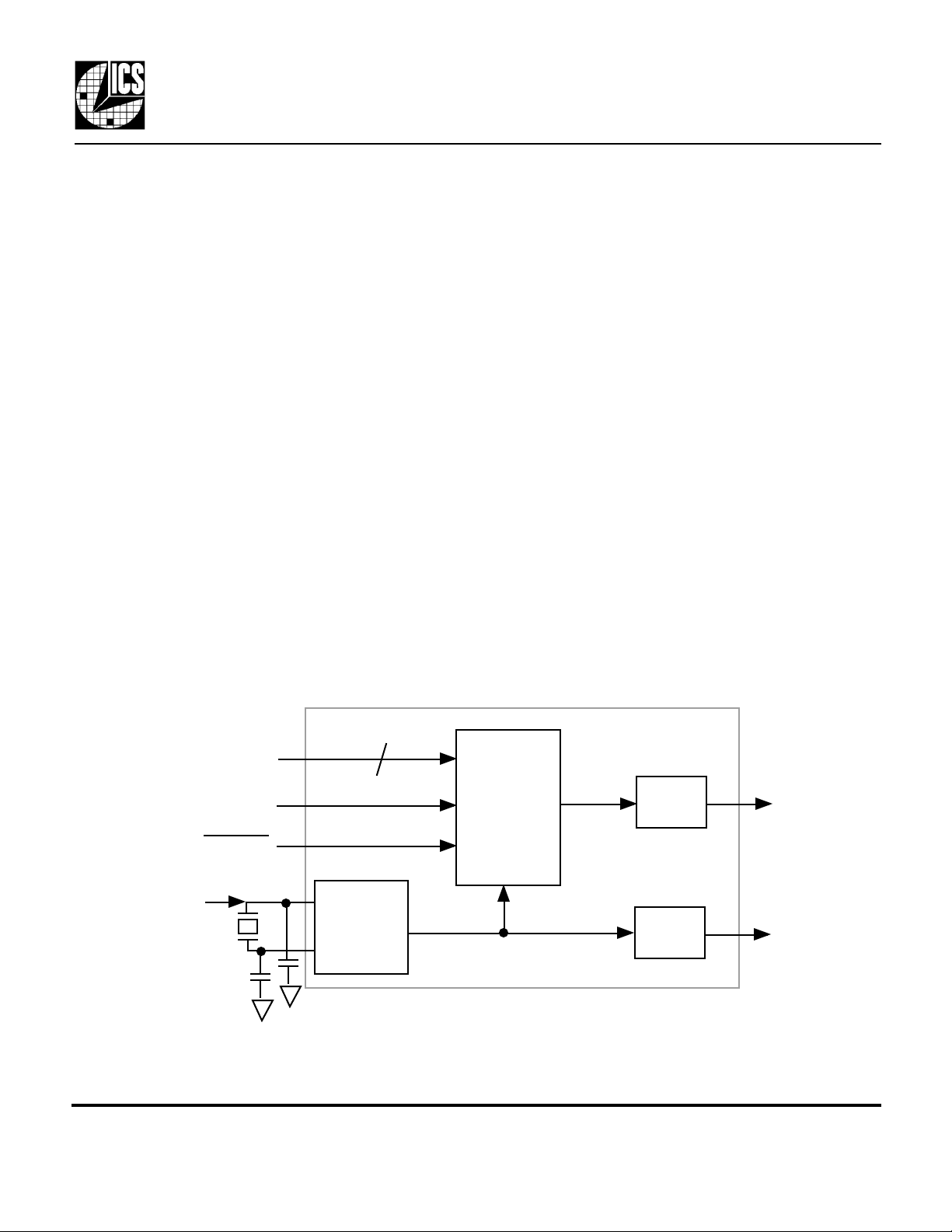
Block Diagram
3.6864 MHz
crystal or clock
S3:S0
REFEN
PDCLK
X1
Crystal
Oscillator
X2
Optional crystal capacitors
4
PLL/Clock
Synthesis
Circuitry
Output
Buffer
Output
Buffer
CLK
REFOUT
MDS 548-05 AC 1 Revision 032900
Integrated Circuit Systems, Inc. • 525 Race Street • San Jose •CA•95126•(408) 295-9800tel • www.icst.com
Page 2
PRELIMINARY INFORMATION
Turns off PLL and stops CLK low
ICS548-05A
MP3 Audio Clock
Pin Assignment
ICS548-05A
X1/ICLK
VDD
VDD
REFEN
GND
GND
S3
S2
Pin Descriptions
1
2
3
4
5
6
7
8
16 pin TSSOP
16
15
14
13
12
11
10
9
X2
DC
REFOUT
S0
S1
PDCLK
DC
CLK
Output Clock Select Table
S3 S2 S1 S0 Input (MHz) CLK (MHz)
Pin 7 Pin 8 Pin 12 Pin 13 Pins 1, (16) Pin 9
0 0 1 0 3.6864 2.8224
0 0 1 1 3.6864 3.072
1 0 0 0 3.6864 4.096
1 0 0 1 3.6864 5.6448
1 0 1 0 3.6864 6.144
1 0 1 1
1 1 0 0 3.6864 8.192
1 1 0 1 3.6864 11.2896
1 1 1 0 3.6864 12.288
1 1 1 1 3.6864 2.048
Power Down Clock Select Table
REFEN PDCLK Power Down Selection Mode
Pin 4 Pin 11
0 0 The entire chip is off.
0 1 PLL and CLK output run, REFOUT low.
1 0 REFOUT running, PLL off, CLK low.
1 1 All running.
Key: 0 = connect directly to GND
1 = connect directly to VDD
Number Name Type Description
1 X1/ICLK XI Crystal connection. Connect to a 3.6864 MHz crystal, or input clock.
2, 3 VDD P Connect to +3.3V or +5V. All VDDs must be same.
4 REFEN I Reference Clock Enable. See above table.
5, 6 GND P Connect to ground.
7 S3 I Frequency select pin 3. Determines clock outputs per table above.
8 S2 I Frequency select pin 2. Determines clock outputs per table above.
9 CLK O Audio clock output set by status of S0-S3. See table above.
10, 15 DC - Don't Connect. Do not connect anything to these pins.
11 PDCLK I Power Down Clock. See above table.
12 S1 I Frequency select pin 1. Determines clock outputs per table above.
13 S0 I Frequency select pin 0. Determines clock outputs per table above.
14 REFOUT O Buffered 3.6864 MHz oscillator output clock. Controlled by REFEN.
16 X2 XO Crystal connection. Connect to a 3.6864 MHz crystal, or leave unconnected for clock.
Key: I = Input; O = output; P = power supply connection; XI, XO = crystal connections
The input pins S3:S0 lack pull-ups, so they cannot be left floating. Tie directly to VDD or GND. For a
clock input, connect the input to X1, and leave X2 unconnected (floating).
MDS 548-05 AC 2 Revision 032900
Integrated Circuit Systems, Inc. • 525 Race Street • San Jose •CA•95126•(408) 295-9800tel • www.icst.com
Page 3

PRELIMINARY INFORMATION
ABSOLUTE MAXIMUM RATINGS (note 1)
DC CHARACTERISTICS (VDD = 3.3V unless noted)
AC CHARACTERISTICS (VDD = 3.3V unless noted)
exposure to levels above the operating limits but below the Absolute Maximums may affect device reliability.
ICS548-05A
MP3 Audio Clock
Electrical Specifications
Parameter Conditions Minimum Typical Maximum Units
Supply voltage, VDD Referenced to GND 7 V
Inputs and Clock Outputs Referenced to GND -0.5 VDD+0.5 V
Ambient Operating Temperature 0 70 °C
Soldering Temperature Max of 10 seconds 260 °C
Storage temperature -65 150 °C
Core Operating Voltage, VDD 2.7 5.5 V
Input High Voltage, VIH, X1/ICLK pin Clock input only (VDD/2)+1 VDD/2 V
Input Low Voltage, VIL, X1/ICLK pin Clock input only VDD/2 (VDD/2)-1 V
Input High Voltage, VIH 2 V
Input Low Voltage, VIL 0.8 V
Output High Voltage, VOH IOH=-12mA 2.4 V
Output Low Voltage, VOL IOL=12mA 0.4 V
Output High Voltage, VOH, CMOS level IOH=-4mA VDD-0.4 V
Operating Supply Current, IDD No Load 4 mA
Power Down Supply Current, IDDPD No Load 5 µA
Short Circuit Current CLK output ±50 mA
Input Capacitance S0, S1, S2, S3, PDCLK 7 pF
Frequency synthesis error All selections 0 ppm
Input Crystal or Clock Frequency 3.6864 MHz
Output Clock Rise Time 0.8 to 2.0V 2 ns
Output Clock Fall Time 2.0 to 0.8V 2 ns
Output Clock Duty Cycle At VDD/2 40 50 60 %
Start-up Time VDD=3V to CLK stable 10 ms
Maximum Absolute Jitter, short term ±250 ps
One sigma jitter 70 ps
Note: 1. Stresses beyond those listed under Absolute Maximum Ratings could cause permanent damage to the device. Prolonged
External Components/ Application Information
The ICS548-05 requires a minimum number of external components for proper operation. A decoupling
capacitor of 0.01µF should be connected between VDD and GND on pins 3 and 5, as close to the
ICS548-05 as possible. Other VDDs can be connected to pin 3. A series termination resistor of 33 Ω may
be used for each clock output. If REFOUT is not used, then REFEN should be connected to ground. The
input crystal must be connected as close to the chip as possible. The input crystal should be fundamental
mode, parallel resonant. For exact accuracy of the output frequencies, the crystal can be tuned with two
identical capacitors to ground, as shown on the block diagram. The value of these two crystal caps should be
equal to (CL-6)*2, where CL is the crystal load (or correlation) capacitance.
MDS 548-05 AC 3 Revision 032900
Integrated Circuit Systems, Inc. • 525 Race Street • San Jose •CA•95126•(408) 295-9800tel • www.icst.com
Page 4

PRELIMINARY INFORMATION
Inches
Millimeters
Package Outline and Package Dimensions
(For current dimensional specifications, see JEDEC publication no. 95.)
16 pin TSSOP
Symbol Min Max Min Max
A -- 0.047 -- 1.19
A1 0.002 0.006 0.05 0.15
b 0.007 0.012 0.18 0.30
c 0.0035 0.008 0.09 0.20
D 0.193 0.201 4.90 5.11
e
E
E1 0.169 0.177 4.29 4.50
L 0.018 0.030 0.46 0.76
INDEX
AREA
E1 E
1 2
D
ICS548-05A
MP3 Audio Clock
A1 c
A
e
b
L
Ordering Information
Part/Order Number Marking Shipping packaging Package Temperature
ICS548G-05 548G-05 tubes 16 pin TSSOP 0-70 °C
ICS548G-05T 548G-05 tape and reel 16 pin TSSOP 0-70 °C
While the information presented herein has been checked for both accuracy and reliability, Integrated Circuit Systems, Incorporated (ICS) assumes no responsibility for either its
use or for the infringement of any patents or other rights of third parties, which would result from its use. No other circuits, patents, or licenses are implied. This product is
intended for use in normal commercial applications. Any other applications such as those requiring extended temperature range, high reliability, or other extraordinary
environmental requirements are not recommended without additional processing by ICS. ICS reserves the right to change any circuitry or specifications without notice. ICS does
not authorize or warrant any ICS product for use in life support devices or critical medical instruments.
MDS 548-05 AC 4 Revision 032900
Integrated Circuit Systems, Inc. • 525 Race Street • San Jose •CA•95126•(408) 295-9800tel • www.icst.com
 Loading...