

Page 1
ICS542
Clock Divider
Description
The ICS542 is a cost effective way to produce a
high quality clock output divided from a clock
input. The chip accepts a clock input up to
156 MHz, and produces a divide by 2, 4, 6, 8, 12,
or 16 of the input clock. There are two outputs on
the chip, one being a low-skew divide by two of
the other. So, for instance, if a 100 MHz clock is
used, the ICS542 can produce low skew 50 MHz
and 25 MHz clocks, or low skew 25 MHz and
12.5 MHz clocks. The chip has an all-chip power
down mode that stops the outputs low, and an OE
pin that tri-states the outputs.
The ICS542 is a member of the ICS
ClockBlocks™ family of clock building blocks.
See the ICS541 and ICS543 for other clock
dividers, and the ICS501, 502, 511, 512 and 525
for clock multipliers.
Features
• Packaged as 8 pin SOIC
• ICS’ lowest cost clock divider
• Low skew (500ps) outputs. One is ÷ 2 of other.
• Easy to use with other generators and buffers
• Input clock frequency up to 156 MHz
• Output clock duty cycle of 45/55
• Power Down turns off chip
• Output Enable
• Advanced, low power CMOS process
• Operating voltages of 3.0 to 5.5 V
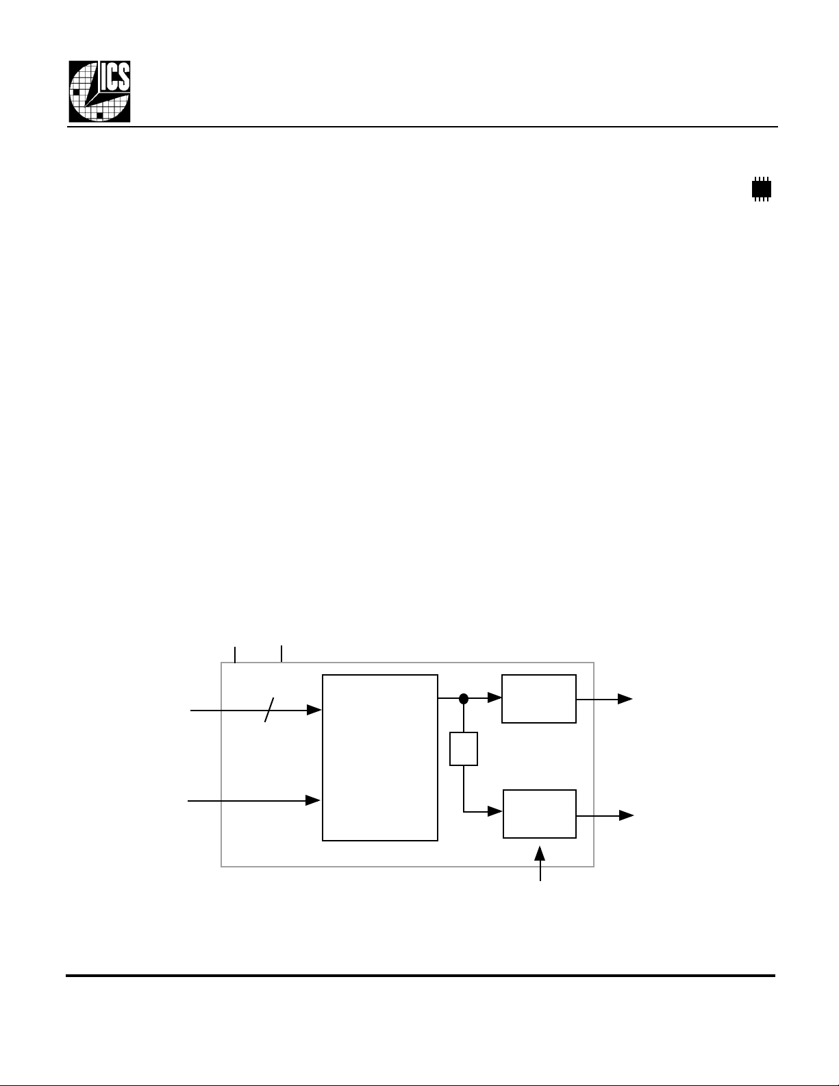
Block Diagram
S1, S0
Input Clock
VDD GND
2
Divider and
Selection
Circuitry
Output
Buffer
÷2
Output
Buffer
OE (both outputs)
CLK
CLK/2
MDS 542 B 1 Revision 050400 Printed 11/14/00
Integrated Circuit Systems, Inc. • 525 Race Street • San Jose •CA•95126• (408) 295-9800tel • www.icst.com
Page 2
ICS542
Power Down All
Clock Divider
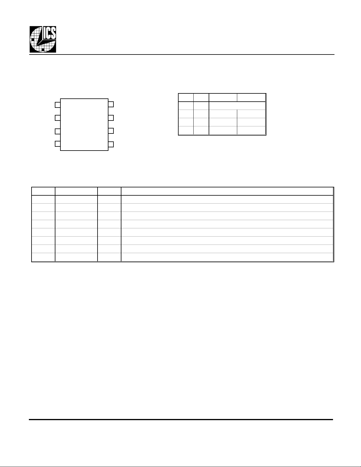
Pin Assignment
ICLK
VDD
GND
S0
1 8
2
3
4
7
6
5
CLK
CLK/2
OE
S1
Clock Decoding Table
S1 S0 CLK CLK/2
0 0
0 1 Input/6 Input/12
1 0 Input/8 Input/16
1 1 Input/2 Input/4
0 = connect directly to ground.
1 = connect directly to VDD.
8 pin SOIC
Pin Descriptions
Number Name Type Description
1 ICLK CI Clock input.
2 VDD P Connect to +3.3V or +5V.
3 GND P Connect to ground.
4 S0 I Select 0 for output clock. Connect to GND or VDD. Internal pull-up.
5 S1 I Select 1 for output clock. Connect to GND or VDD. Internal pull-up.
6 OE I Output Enable. Tri-states both output clocks when low. Internal pull-up.
7 CLK/2 O Clock output per Table above. Low skew divide by two of pin 8 clock.
8 CLK O Clock output per Table above.
Key: CI = clock input, I = input, O = output, P = power supply connection
External Components
The ICS542 requires a 0.01 µF decoupling capacitor to be connected between VDD and GND. It must
be connected close to the ICS542 to minimize lead inductance. No external power supply filtering is
required for this device. A 33 Ω series terminating resistor can be used next to each output pin. If a 3.3 V
input clock is applied to the ICLK pin, with the ICS542 at 5 V, the clock must be AC coupled.
MDS 542 B 2 Revision 050400 Printed 11/14/00
Integrated Circuit Systems, Inc. • 525 Race Street • San Jose •CA•95126• (408) 295-9800tel • www.icst.com
Page 3

ICS542
ABSOLUTE MAXIMUM RATINGS (stresses beyond these can permanently damage the device)
DC CHARACTERISTICS (VDD = 3.3V unless otherwise noted)
AC CHARACTERISTICS (VDD = 3.3V unless otherwise noted)
Clock Divider
Electrical Specifications
Parameter Conditions Minimum Typical Maximum Units
Supply Voltage, VDD Referenced to GND 7 V
Inputs Referenced to GND -0.5 VDD+0.5 V
Clock Output Referenced to GND -0.5 VDD+0.5 V
Ambient Operating Temperature 0 70 C
Soldering Temperature Max of 10 seconds 260 C
Storage temperature -65 150 C
Operating Voltage, VDD 3 5.5 V
Input High Voltage, VIH, ICLK only ICLK (Pin 1) (VDD/2)+1 VDD/2 V
Input Low Voltage, VIL, ICLK only ICLK (Pin 1) VDD/2 (VDD/2)-1 V
Input High Voltage, VIH S0, S1, OE 2 V
Input Low Voltage, VIL S0, S1, OE 0.8 V
Output High Voltage, VOH, CMOS levels IOH=-4mA VDD-0.4 V
Output High Voltage, VOH IOH=-12mA 2.4 V
Output Low Voltage, VOL IOL=4mA 0.4 V
IDD Operating Supply Current, 100 MHz input No Load, 5.0V, 11 sel 11 mA
IDD Operating Supply Current, 100 MHz input No Load, 3.3V, 11 sel 7 mA
Short Circuit Current Each Output ±40 mA
Input Capacitance, S1, S0, OE Pins 4, 5, 6 4 pF
Input Frequency, clock input at VDD = 5V 0 156 MHz
Input Frequency, clock input at VDD = 3.3V 0 156 MHz
Skew of output clocks rising edges at VDD/2 500 ps
Output Clock Rise Time 0.8 to 2.0V 1 ns
Output Clock Fall Time 2.0 to 0.8V 1 ns
Output Clock Duty Cycle at VDD/2 45 49 to 51 55 %
MDS 542 B 3 Revision 050400 Printed 11/14/00
Integrated Circuit Systems, Inc. • 525 Race Street • San Jose •CA•95126• (408) 295-9800tel • www.icst.com
Page 4

Package Outline and Package Dimensions
Inches
Millimeters
E H
INDEX
AREA
1 2
h x 45°
D
ICS542
Clock Divider
8 pin SOIC
Symbol Min Max Min Max
A 0.0532 0.0688 1.35 1.75
A1
D 0.1890 0.1968 4.80 5.00
H 0.2284 0.2440 5.80 6.20
0.0040 0.0098 0.10 0.24
B 0.0130 0.0200 0.33 0.51
C
0.0075 0.0098 0.19 0.24
E 0.1497 0.1574 3.80 4.00
e
h 0.0099 0.0195 0.25 0.50
L 0.0160 0.0500 0.41 1.27
A1 C
A
e
B
L
Ordering Information
Part/Order Number Marking Package Temperature
ICS542M ICS542M 8 pin SOIC 0 to 70 °C
ICS542MT ICS542M 8 pin SOIC on tape and reel 0 to 70 °C
While the information presented herein has been checked for both accuracy and reliability, ICS/MicroClock assumes no responsibility for either its use or for the infringement of
any patents or other rights of third parties, which would result from its use. No other circuits, patents, or licenses are implied. This product is intended for use in normal
commercial applications. Any other applications such as those requiring extended temperature range, high reliability, or other extraordinary environmental requirements are not
recommended without additional processing by ICS/MicroClock. ICS/MicroClock reserves the right to change any circuitry or specifications without notice. ICS/MicroClock
does not authorize or warrant any ICS/MicroClock product for use in life support devices or critical medical instruments.
ClockBlocks is a trademark of ICS
MDS 542 B 4 Revision 050400 Printed 11/14/00
Integrated Circuit Systems, Inc. • 525 Race Street • San Jose •CA•95126• (408) 295-9800tel • www.icst.com
 Loading...