

Page 1
User Configurable Zero Delay Buffer
Description Features
The ICS527-01 Clock Slicer™ is the most flexible
way to generate an output clock from an input
clock with zero skew. The user can easily configure
the device to produce nearly any output clock that
is multiplied or divided from the input clock. The
part supports non-integer multiplications and
divisions. A SYNC pulse indicates the rising clock
edges that are aligned with zero skew. Using
Phase-Locked Loop (PLL) techniques, the device
accepts an input clock up to 200 MHz and
produces an output clock up to 160 MHz.
The ICS527-01 aligns rising edges on ICLK and
FBIN at a ratio determined by the reference and
feedback dividers.
For configurable clocks that do not require
zero delay, use the ICS525.
• Packaged as 28 pin SSOP (150 mil body)
• Synchronizes fractional clocks rising edges
• User determines the output frequency - no
software needed
• Slices frequency or period
• SYNC pulse output indicates aligned edges
• Input clock frequency of 600 kHz - 200 MHz
• Output clock frequencies up to 160 MHz
• Very low jitter
• Duty cycle of 45/55 up to 160 MHz
• Operating voltage of 3.3 V (±10%)
• Pin selectable double drive strength
• Multiple outputs available when combined with
Buffalo clock drivers
ICS527-01
Clock Slicer™
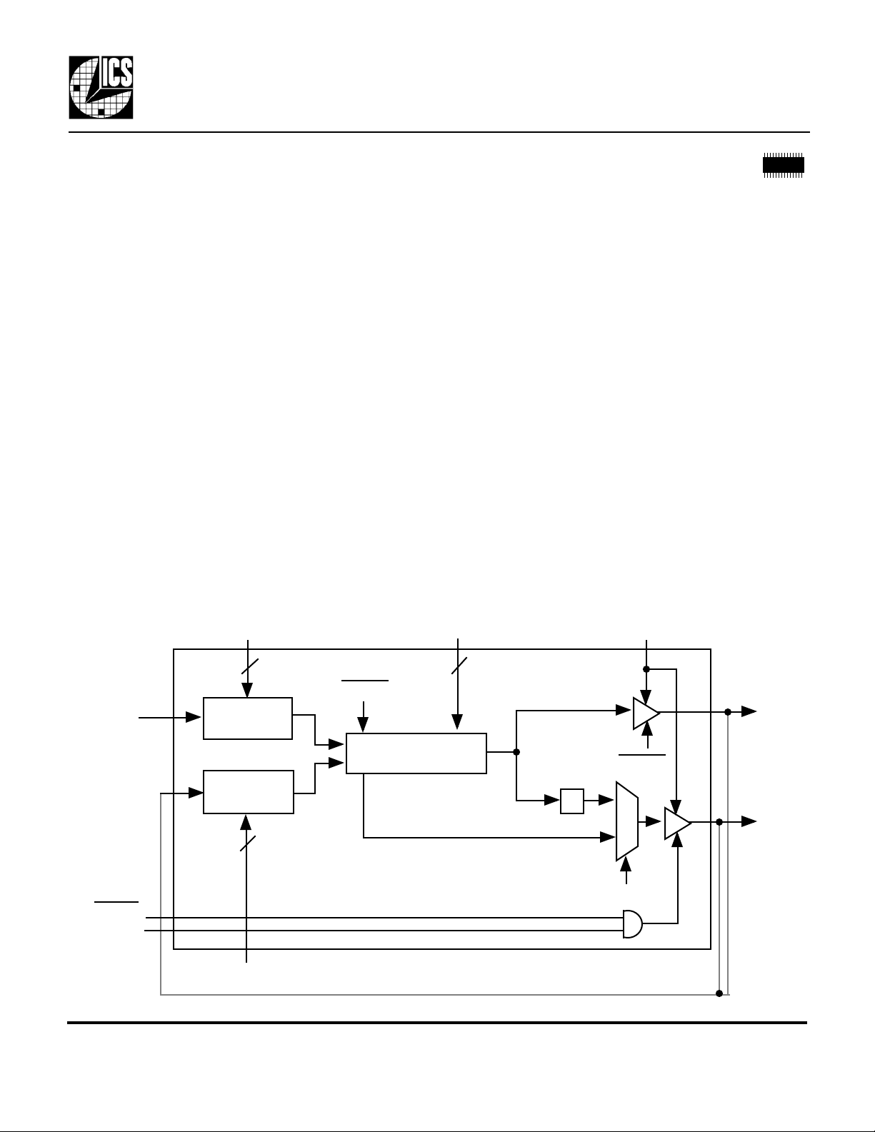
Block Diagram
ICLK
FBIN
PDTS
OECLK2
R6:R0
7
Reference
Divide
Feedback
Divide
7
PDTS
PLL
• Zero input to output skew
• Industrial temperature version available
• Advanced, low power CMOS process
S1:S0
2
÷2
SYNC
2XDRIVE
PDTS
1
0
DIV2
CLK1
CLK2
F6:F0
MDS 527-01 B 1 Revision 020801
Integrated Circuit Systems, Inc. • 525 Race Street • San Jose • CA•95126•(408)295-9800tel • www.icst.com
External feedback from CLK1 or CLK2 (not both).
Page 2
ICS527-01
CLK1 Output Frequency (MHz)
Clock Slicer™
User Configurable Zero Delay Buffer
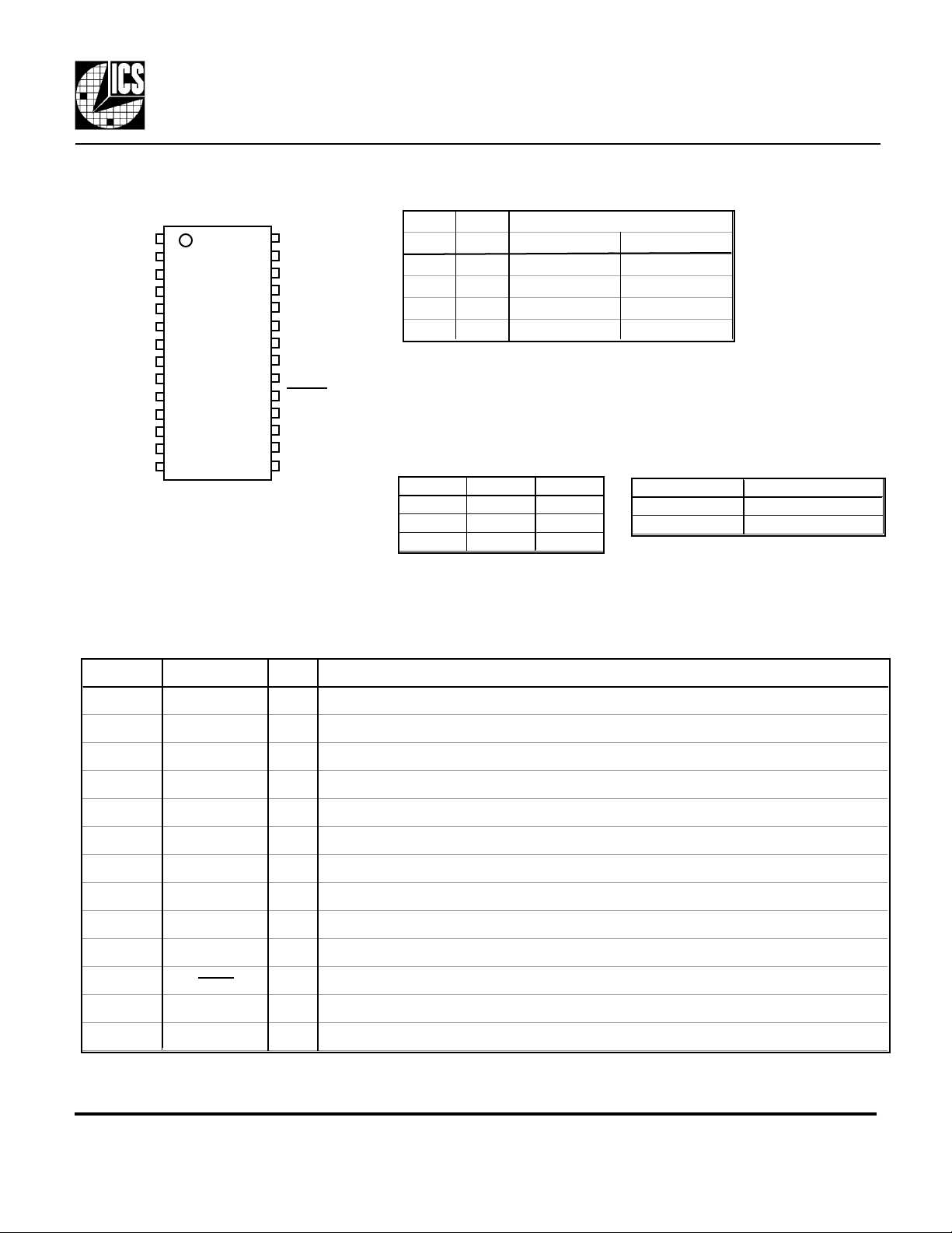
Pin Assignment
R5
1
2
R6
S0
S1
F0
F1
F2
3
4
5
6
7
8
9
10
11
12
13
14
DIV2
VDD
ICLK
FBIN
GND
OECLK2
2XDRIVE
Pin Description
28
27
26
25
24
23
22
21
20
19
18
17
16
15
R4
R3
R2
R1
R0
VDD
CLK1
CLK2
GND
PDTS
F6
F5
F4
F3
Frequency Configuration Table
S1 S0
pin 5 pin 4 0 to 70° -40 to 85°
0 0 37 - 75 35 - 70
0 1 18 - 37 16 - 35
1 0 4 - 10 4 - 8
1 1 75 - 160 70 - 140
To cover the range from 10-18 MHz (0-70 °C) and 8-16
(-40-85°C), select address 01 to generate 2x your desired output
frequency, then configure CLK2 to generate CLK1/2
CLK2 Operation Table
OECLK2 DIV2 CLK2
0 X Z
1 0 SYNC
1 1 CLK1/2
Clock Drive Select Table
2XDRIVE OUTPUT DRIVE
0 12 mA
1 25 mA
Pin # Name Type Description
1, 2, 24-28 R5, R6, R0-R4 I(PU) Reference divider word input pins determined by user. Forms a binary number from 0 to 127.
3 DIV2 I(PU) Selects CLK2 function to output a SYNC signal or a divide by 2 of CLK1. See table above.
4, 5 S0, S1 I(PU) Select pins for output divider determined by user. See table above.
6, 23 VDD P Connect to VDD.
7 ICLK I Reference clock input.
8 FBIN I Feedback clock input.
9, 20 GND P Connect to ground.
10 OECLK2 I(PU) CLK2 Output Enable. CLK2 tri-stated when low.
11 2XDRIVE I(PU) Clock output drive strength doubled when high.
12-18 F0-F6 I(PU) Feedback divider word input pins determined by user. Forms a binary number from 0 to 127.
19 PDTS I(PU) Power Down. Active low. Turns off entire chip when low. Both Clock outputs tri-stated.
21 CLK2 O Output Clock 2. Can be the SYNC output or a low skew divide by 2 of CLK1.
22 CLK1 O Output Clock 1.
Key: I = Input; I(PU) = Input with internal pull-up resistor; I = Input; O = Output; P = Power supply
connection
MDS 527-01 B 2 Revision 020801
Integrated Circuit Systems, Inc. • 525 Race Street • San Jose • CA•95126•(408)295-9800tel • www.icst.com
Page 3
ICS527-01
Clock Slicer™
User Configurable Zero Delay Buffer
Using the Clock Slicer™
First use DIV2 to select the function of the CLK2 output. If DIV2 is high, a divide-by-2, low skew version
of CLK1 is present on CLK2. If DIV2 is low, a SYNC pulse is generated on CLK2. The SYNC pulse goes
high synchronously with the rising edges of ICLK and CLK1 that are de-skewed. The SYNC function
operates at CLK1 frequencies up to 66 MHz. If neither CLK1/2 or a SYNC pulse are required, then CLK2
should be disabled by connecting OECLK2 to ground, which will also give the lowest jitter on CLK1.
Next, the feedback scheme should be chosen. If CLK2 is being used as a SYNC or is tri-stated, then CLK1
must be connected to FBIN. If CLK2 is selected to be CLK1 divided-by-2 (DIV2 = 1, OECLK2 = 1),
then either CLK1 or CLK2 must be connected to FBIN. The choice between CLK1 or CLK2 is illustrated
by the following example where the device has been configured to generate CLK1 that is twice the
frequency on ICLK.
ICLK
CLK1
CLK2
CLK1 Feedback
Using CLK1 as the feedback will always result in synchronized rising edges between ICLK and CLK1. But
CLK2 could be a falling edge compared with ICLK. Therefore, wherever possible, we recommend the use
of CLK2 feedback. This will synchronize the rising edges of all 3 clocks.
More complicated feedback schemes can be used, such as incorporating multiple output buffers in the
feedback path. An example of this is given later in the datasheet. The fundamental property of the
ICS527-01 is that it aligns rising edges on ICLK and FBIN at a ratio determined by the reference and
feedback dividers.
The drive strength is selected by the 2XDRIVE pin. If high drive strength is not required, we recommend
tying this pin low.
Lastly, the divider settings should be selected. The following section describes how the dividers can be set.
ICLK
CLK1
CLK2
CLK2 Feedback
MDS 527-01 B 3 Revision 020801
Integrated Circuit Systems, Inc. • 525 Race Street • San Jose • CA•95126•(408)295-9800tel • www.icst.com
Page 4

ICS527-01
Clock Slicer™
User Configurable Zero Delay Buffer
Determining (setting) the ICS527-01 Dividers
The user has full control in setting the desired output clocks over the range shown in the table on page 2. The
user should connect the divider select input pins directly to ground (or VDD, although this is not required
because of internal pull-ups) during Printed Circuit Board layout, so that the ICS527-01 automatically
produces the correct clock when all components are soldered. It is also possible to connect the inputs to
parallel I/O ports to switch frequencies.
The output of the ICS527-01 can be determined by the following simple equation:
FB frequency = Input frequency •
Where Reference Divider Word (RDW) = 0 to 127
Feedback Divider Word (FDW) = 0 to 127
FB frequency is the same as either CLK1 or CLK2 depending on
feedback connection
Also, the following operating ranges should be observed:
(FDW+2)
(RDW+2)
300 kHz <
The output divide should be selected depending on the frequency of CLK1.
The table on page 2 gives the ranges.
The dividers are expressed as integers. For example, if a 50 MHz output on CLK1 is desired from a
40 MHz input, the reference divider word (RDW) should be 2 and the feedback divider (FDW) should be
3 which gives the required 5/4 multiplication. If multiple choices of divider are available, then the lowest
numbers should be used. In this example, the output divide (OD) should be selected to be 2. Then R6:R0
is 0000010, F6:F0 is 0000011 and S1:S0 is 00. Also, this example assumes CLK1 is connected to FBIN.
You may also fax this page to MicroClock/ICS at 408 295-9818, or send an e-mail to ics-mk@icst.com.
Be sure to indicate the following:
Your Name ________________ Company Name___________________ Telephone_________________
Respond by e-mail (list your e-mail address) __________________or fax number ___________________
Desired input clock (in MHz) _______________ Desired output frequency________________
Input Frequency
(RDW+2)
MDS 527-01 B 4 Revision 020801
Integrated Circuit Systems, Inc. • 525 Race Street • San Jose • CA•95126•(408)295-9800tel • www.icst.com
Page 5

ICS527-01
Clock Slicer™
User Configurable Zero Delay Buffer
Typical Example
The following connection diagram shows the implementation of the example from the previous section.
This will generate a 50 MHz clock synchronously with a 40 MHz input. A SYNC pulse is desired and the
1x output drive is selected.
VDD
40 MHz
R5
R6
DIV2
0.01 µF 0.01 µF
S0
S1
VDD
ICLK
FBIN
GND GND
OECLK2
2XDRIVE
F0
F1
F2
R4
R3
R2
R1
R0
VDD
33Ω
CLK1
CLK2
33Ω
PDTS
F6
F5
F4
F3
50 MHz
SYNC
Note that the feedback is done AFTER the series termination resistor.
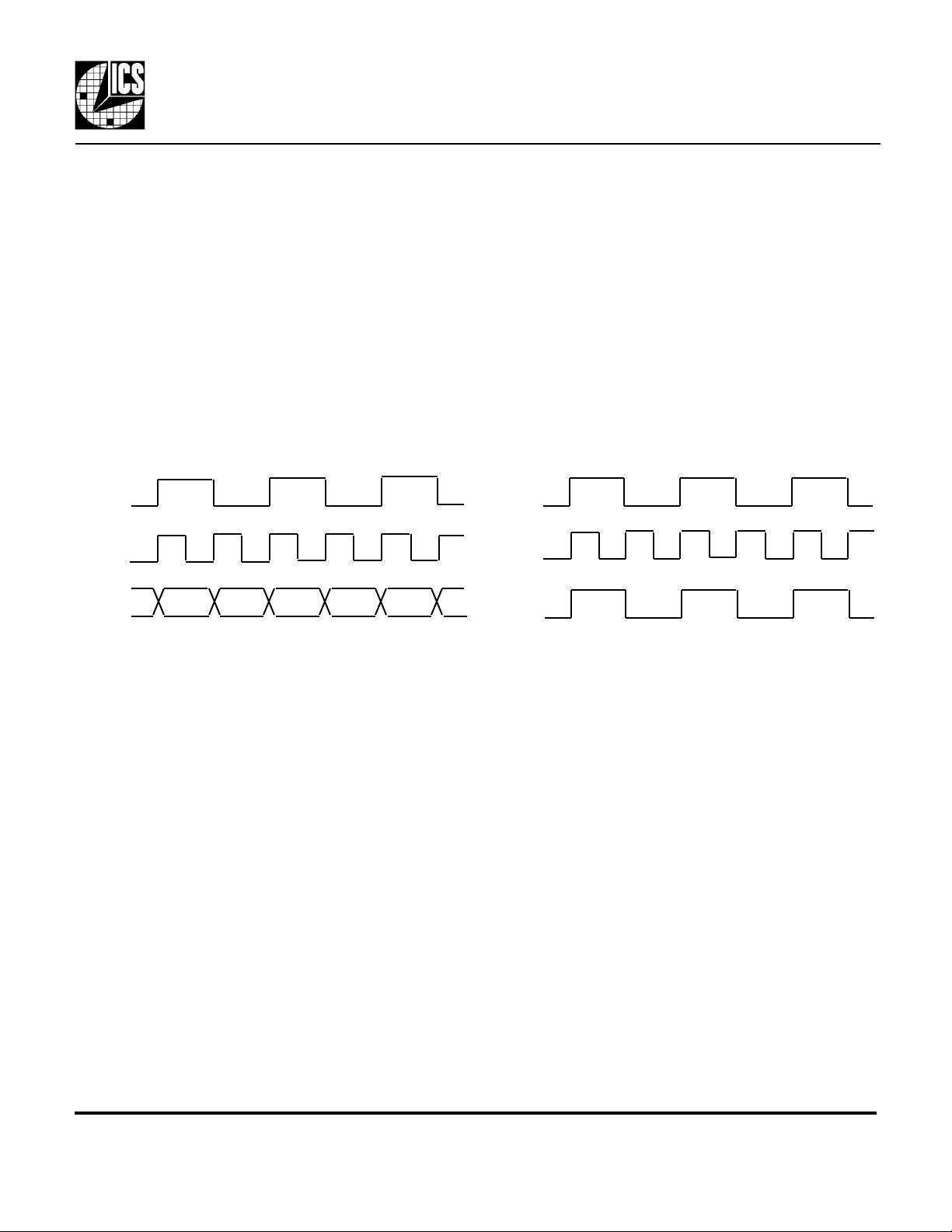
This will give the following waveforms:
40 MHz ICLK
50 MHz CLK1
SYNC CLK2
MDS 527-01 B 5 Revision 020801
Integrated Circuit Systems, Inc. • 525 Race Street • San Jose • CA•95126•(408)295-9800tel • www.icst.com
Page 6

ICS527-01
Clock Slicer™
User Configurable Zero Delay Buffer
Multiple Output Example
In this example, an input clock of 125 MHz is used. Eight copies of 50 MHz are required as are eight
copies of 25 MHz, de-skewed and aligned to the 125 MHz input clock. The following solution uses the
MK74CB217 which has dual 1 to 8 buffers with low pin to pin skew.
VDD
125 MHz
25 MHz
0.01 µF
R5
R6
DIV2
S0
S1
VDD
ICLK
FBIN
GND
OECLK2
2XDRIVE
F0
F1
F2
R4
R3
R2
R1
R0
VDD
CLK1
CLK2
GND
PDTS
F6
F5
F4
F3
0.01 µF
This configuration produces the following waveforms:
125 MHz, ICLK
0.01
µF
INA
QA0
QA1
QA2
VDD
VDD
QA3
QA4
GND GND
GND
QA5
QA6
QA7
OEA
INB
QB0
QB1
QB2
VDD
VDD
QB3
QB4
GND
QB5
QB6
QB7
OEB
0.01 µF
25 MHz, QA0-7
50 MHz, QB0-7
Using the equation for selecting the dividers gives:
25 MHz = 125 MHz • (FDW + 2)
(RDW + 2)
If FDW = 0, then RDW = 8. This gives the required divide-by-5 function. Setting pin DIV2 = 1 gives
both a 25 MHz and 50 MHz output from the ICS527-01. The FBIN pin is connected to the QA7 output
of the MK74CB217. This aligns all the outputs of the MK74CB217 with the 125 MHz input since the
ICS527-01 aligns rising edges on the ICLK and FBIN pins.
In this example, series termination resistors have been omitted for clarity but should be used on all clock
outputs.
MDS 527-01 B 6 Revision 020801
Integrated Circuit Systems, Inc. • 525 Race Street • San Jose • CA•95126•(408)295-9800tel • www.icst.com
Page 7

ICS527-01
ABSOLUTE MAXIMUM RATINGS (stresses beyond these can permanently damage the device)
DC CHARACTERISTICS (VDD = 3.3V unless otherwise noted)
AC CHARACTERISTICS (VDD = 3.3V unless otherwise noted)
Clock Slicer™
User Configurable Zero Delay Buffer
Electrical Specifications
Parameter Conditions Minimum Typical Maximum Units
Supply Voltage, VDD Referenced to GND 7 V
Inputs Referenced to GND -0.5 VDD+0.5 V
Clock Output Referenced to GND -0.5 VDD+0.5 V
Ambient Operating Temperature ICS527R-01 0 70 °C
ICS527R-01I -40 85 °C
Soldering Temperature Max of 10 seconds 260 °C
Storage Temperature -65 150 °C
Operating Voltage, VDD 3 3.6 V
Input High Voltage, VIH 2 V
Input Low Voltage, VIL 0.8 V
Input High Voltage, VIH, ICLK and FBIN pins 7, 8 (VDD/2)+1 V
Input Low Voltage, VIL, ICLK and FBIN pins 7, 8 (VDD/2)-1 V
Output High Voltage, VOH (2X DRIVE = 0) IOH=-12mA 2.4 V
Output Low Voltage, VOL (2X DRIVE = 0) IOL=12mA 0.4 V
Output High Voltage, VOH (2X DRIVE = 1) IOH=-25mA 2.4 V
Output Low Voltage, VOL (2X DRIVE = 1) IOL=25mA 0.4 V
IDD Operating Supply Current, 15 MHz IN 60MHz out, no load 8 mA
IDD Operating Supply Current, Power Down 20 µA
Short Circuit Current (2XDRIVE = 0) CLK outputs ±70 mA
Short Circuit Current (2XDRIVE = 1) CLK outputs ±140 mA
On-Chip Pull-up Resistor 270 kΩ
Input Capacitance 4 pF
Input Frequency, clock input 0.6 200 MHz
Output Frequency, CLK1 0 C to 70 °C 4 160 MHz
-40 C to +85 °C 4 140 MHz
CLK1 Frequency for correct SYNC operation 66 MHz
Output Clock Rise Time 0.8 to 2.0V 1 ns
Output Clock Fall Time 2.0 to 0.8V 1 ns
Output Clock Duty Cycle at VDD/2, 15 pF load 45 50 55 %
Power Down Time,PDTS low to clocks tri-stated 50 ns
Power Up Time, PDTS high to clocks stable 10 ms
Absolute Clock Period Jitter Deviation from mean ±90 ps
One Sigma Clock Period Jitter 40 ps
Skew of output clocks, CLK1 to CLK2 Note 1 -250 0 250 ps
Input to output skew, ICLK to FBIN Note 1 -250 0 250 ps
Device to device skew, common ICLK at FBIN 0 500 ps
Note 1: Assumes clocks with same rise time, measured from rising edges at VDD/2.
MDS 527-01 B 7 Revision 020801
Integrated Circuit Systems, Inc. • 525 Race Street • San Jose • CA•95126•(408)295-9800tel • www.icst.com
Page 8

ICS527-01
Inches
Millimeters
Clock Slicer™
User Configurable Zero Delay Buffer
External Components
The ICS527-01 requires two 0.01µF decoupling capacitors to be connected between VDD and GND, one
on each side of the chip. They must be connected close to the device to minimize lead inductance. No
external power supply filtering is required for this device. A 33Ω series terminating resistor can be used
next to the CLK1 and CLK2 pins.
Package Outline and Package Dimensions
(For current dimensional specifications, see JEDEC no. 95.)
28 pin SSOP
Symbol Min Max Min Max
A 0.053 0.069 1.35 1.75
A1 0.004 0.010 0.10 0.25
b 0.008 0.012 0.20 0.30
c 0.007 0.010 0.19 0.25
D 0.386 0.394 9.80 10.01
e
E 0.228 0.244 5.79 6.20
E1 0.150 0.157 3.81 3.99
L 0.016 0.050 0.41 1.27
INDEX
AREA
E1 E
1 2
D
A1 c
A
e
b
L
Ordering Information
Part/Order Number Marking Package Temperature
ICS527R-01 ICS527R-01 28 pin narrow SSOP 0 to 70 °C
ICS527R-01T ICS527R-01 28 pin SSOP on tape and reel 0 to 70 °C
ICS527R-01I ICS527R-01I 28 pin narrow SSOP -40 to 85 °C
ICS527R-01IT ICS527R-01I 28 pin SSOP on tape and reel -40 to 85 °C
While the information presented herein has been checked for both accuracy and reliability, Integrated Circuit Systems assumes no responsibility for either its use or for the
infringement of any patents or other rights of third parties, which would result from its use. No other circuits, patents, or licenses are implied. This product is intended for use in
normal commercial applications. Any other applications such as those requiring extended temperature range, high reliability, or other extraordinary environmental requirements
are not recommended without additional processing by ICS. ICS reserves the right to change any circuitry or specifications without notice. ICS does not authorize or warrant any
ICS/MicroClock product for use in life support devices or critical medical instruments.
MDS 527-01 B 8 Revision 020801
Integrated Circuit Systems, Inc. • 525 Race Street • San Jose • CA•95126•(408)295-9800tel • www.icst.com
 Loading...