

Page 1
PR EL I MI NA RY IN FO R MA TI ON
PECL to CMOS Converter
Description Features
ICS508
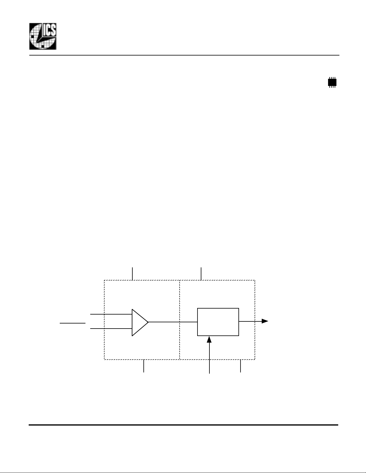
The ICS508 is the most cost effective way to
generate a high quality, high frequency CMOS
clock output from a PECL clock input.
The ICS508 has separate VDD supplies for the
PECL input buffer and the output buffer allowing
different voltages to be used. For example, the
input clock could use a 3.3 V supply while the
output operates from 2.5 V.
The device has an Output Enable pin that tri-states
the clock output when the OE pin is taken low.
The ICS508 is a member of the ClockBlocks™
family of devices.
Block Diagram
• Packaged as 8 pin SOIC or die
• Separate VDD supplies allow voltage
translation
• Clock frequency of 0 - 250 MHz
• Duty cycle of 45/55
• Operating voltages of 2.375 to 5.5 V
• Tri-state output for board level testing
• 24 mA drive capability
• Industrial temperature version available
• Advanced, low power CMOS process
VDDP VDDC
PECLIN
PECLIN
GND
MDS 508 C 1 Revision 012400 Printed 11/13/00
Integrated Circuit Systems, Inc. • 525 Race Street • San Jose •CA•95126•(408) 295-9800tel • www.icst.com
Output
Buffer
OE
CLK
GND
Page 2
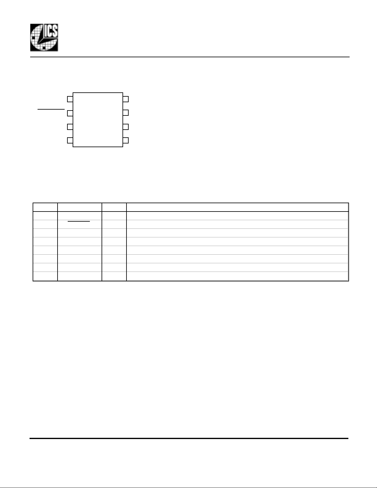
Pin Assignment
PR EL I MI NA RY IN FO R MA TI ON
ICS508
PECL to CMOS Converter
VDDP
PECLIN
PECLIN
GND
18
2
3
4
VDDC
7
CLK
6
GND
5
OE
Pin Descriptions
Number Name Type Description
1 VDDP O Connect to 3.3 V or 5 V. Supplies PECL input buffer.
2 I Complementary PECL clock input.
3 PECLIN I
4 GND P Connect to ground.
5 OE I Output enable. Tri-states CLK output when low. Internal pull-up to VDDC.
6 GND P Connect to ground.
7 CLK O Clock output.
8 VDDC P Connect to 2.5 V, or 3.3 V or 5 V. Supplies output buffer and OE pin.
PECLIN
PECL clock input.
Key: I = Input, O = output, P = power supply connection
MDS 508 C 2 Revision 012400 Printed 11/13/00
Integrated Circuit Systems, Inc. • 525 Race Street • San Jose •CA•95126•(408) 295-9800tel • www.icst.com
Page 3

PR EL I MI NA RY IN FO R MA TI ON
t
t
t
t
ICS508
PECL to CMOS Converter
Electrical Specifications
Parameter Conditions Minimum Typical Maximum Units
ABSOLUTE MAXIMUM RATINGS (s
Supply Voltage, VDDP and VDDC Referenced to GND 7 V
PECL Inputs Referenced to GND -0.5 VDDP+0.5 V
Clock Output and OE Pin Referenced to GND -0.5 VDDC+0.5 V
Ambient Operating Temperature 0 70 °C
Soldering Temperature Max of 10 seconds 260 °C
Storage temperature -65 150 °C
DC CHARACTERISTICS (VDDP = VDDC = 3.3 V unless otherwise noted)
Operating Voltage, VDDP
Operating Voltage, VDDC
Peak to Peak Input Voltage, PECLIN 0.3 1 V
Common Mode Range, PECLIN
Common Mode Range, PECLIN
Input High Voltage, VIH
Input Low Voltage, VIL
Output High Voltage, VOH
Output High Voltage, VOL
Output High Voltage, VOH
Output High Voltage, VOL
Output High Voltage, VOH
Output High Voltage, VOL
On-Chip Pull-up Resistor
Operating Supply Current, IDDP 100 MHz, no load 1.5 mA
Operating Supply Current, IDDC 100 MHz, no load 8 mA
Note 1: VDDP must alwa s be greater than or equal to VDDC.
resses beyond these can permanently damage
ICS508MI only -40 85 °C
Note 1
Note 1
VDDP = 5 V
VDDP = 3.3 V
OE only
OE only
VDDC = 5 V, IOH = -24 mA
VDDC = 5 V, IOL = 24 mA
VDDC = 3.3 V, IOH = -18 mA
VDDC = 3.3 V, IOL = 18 mA
VDDC = 2.5 V, IOH = -8 mA
VDDC = 2.5 V, IOL = 8 mA
OE
3 5.5 V
2.375 5.5 V
VDDP - 3.7 VDDP - 0.6 V
VDDP - 2.0 VDDP - 0.6 V
2 VDDC V
VDDC-0.4 V
VDDC-0.4 V
VDDC-0.4 V
250 kΩ
he device)
0.8 V
0.4 V
0.4 V
0.4 V
MDS 508 C 3 Revision 012400 Printed 11/13/00
Integrated Circuit Systems, Inc. • 525 Race Street • San Jose •CA•95126•(408) 295-9800tel • www.icst.com
Page 4

PR EL I MI NA RY IN FO R MA TI ON
ICS508
PECL to CMOS Converter
Electrical Specifications
Parameter Conditions Minimum Typical Maximum Units
AC CHARACTERISTICS (VDDP = VDDC = 3.3V unless otherwise noted)
Input Frequency 0 250 MHz
Output Clock Rise Time, 0.8 to 2 V
Output Clock Fall Time, 2 V to 0.8 V
Output Enable Time, OE high to ouput on 7 20 ns
Output Disable Time, OE low to tri-state 7 20 ns
Propagation Delay
Output Clock Duty Cycle, 0-100 MHz Any VDD combination 45 55 %
Output Clock Duty Cycle, 100-166 MHz
Output Clock Duty Cycle, 166-250 MHz
VDDC = 5 V
VDDC = 3.3 V
VDDC = 2.5 V
VDDC = 5 V
VDDC = 3.3 V
VDDC = 2.5 V
VDDP=5 V, VDDC=5 V
VDDP=5 V, VDDC=3.3 V
VDDP=5 V, VDDC=2.5 V
VDDP=3.3 V, VDDC=3.3 V
VDDP=3.3 V, VDDC=2.5 V
VDDP=5 V, VDDC=5 V
VDDP=5 V, VDDC=3.3 V
VDDP=5 V, VDDC=2.5 V
VDDP=3.3 V, VDDC=3.3 V
VDDP=3.3 V, VDDC=2.5 V
VDDP=5 V, VDDC=5 V
VDDP=5 V, VDDC=3.3 V
VDDP=5 V, VDDC=2.5 V
VDDP=3.3 V, VDDC=3.3 V
VDDP=3.3 V, VDDC=2.5 V
0.4 ns
0.6 ns
1 ns
0.4 ns
0.6 ns
1 ns
4 6 ns
4.5 7 ns
5.5 9 ns
4.5 7 ns
5.5 9 ns
45 55 %
45 55 %
40 60 %
40 60 %
45 55 %
40 60 %
40 60 %
35 65 %
35 65 %
40 60 %
MDS 508 C 4 Revision 012400 Printed 11/13/00
Integrated Circuit Systems, Inc. • 525 Race Street • San Jose •CA•95126•(408) 295-9800tel • www.icst.com
Page 5

PR EL I MI NA RY IN FO R MA TI ON
g
ICS508
PECL to CMOS Converter
External Components
The ICS508 requires two 0.01µF decoupling capacitors to be connected between VDDP and GND and
between VDDC and GND. They must be connected close to the ICS508 to minimize lead inductance. A
33 Ω series terminatin
Package Outline and Package Dimensions
(
For current dimensional specifications, see JEDEC Publication No. 95.)
INDEX
AREA
12
resistor can be used next to the CLK pin.
EH
h x 45°
D
8 pin SOIC
Inches Millimeters
Symbol Min Max Min Max
A 0.0532 0.0688 1.35 1.75
A1
D 0.1890 0.1968 4.80 5.00
H 0.2284 0.2440 5.80 6.20
0.0040 0.0098 0.10 0.24
B 0.0130 0.0200 0.33 0.51
C
0.0075 0.0098 0.19 0.24
E 0.1497 0.1574 3.80 4.00
e .050 BSC 1.27 BSC
h 0.0099 0.0195 0.25 0.50
L 0.0160 0.0500 0.41 1.27
A1
e
C
B
A
L
Ordering Information
Part/Order Number Marking Package Temperature
ICS508M ICS508M 8 pin SOIC 0 to 70 °C
ICS508MT ICS508M 8 pin SOIC on tape and reel 0 to 70 °C
ICS508MI ICS508I 8 pin SOIC -40 to +85 °C
ICS508MIT ICS508I 8 pin SOIC on tape and reel -40 to +85 °C
ICS508-DWF - Die on uncut, probed wafers 0 to 70 °C
ICS508-DPK - Tested die in waffle pack 0 to 70 °C
While the information presented herein has been checked for both accuracy and reliability, ICS assumes no responsibility for either its use or for the infringement of any patents or
other rights of third parties, which would result from its use. No other circuits, patents, or licenses are implied. This product is intended for use in normal commercial applications.
Any other applications such as those requiring extended temperature range, high reliability, or other extraordinary environmental requirements are not recommended without
additional processing by ICS. ICS reserves the right to change any circuitry or specifications without notice. ICS does not authorize or warrant any ICS product for use in life support
devices or critical medical instruments.
MDS 508 C 5 Revision 012400 Printed 11/13/00
Integrated Circuit Systems, Inc. • 525 Race Street • San Jose •CA•95126•(408) 295-9800tel • www.icst.com
 Loading...