

Datasheet ICS507M-01, ICS507M-01-DPK, ICS507M-01-DSW, ICS507M-01I, ICS507M-01IT Datasheet (ICST)
...Page 1
ICS507-01/02
PECL Clock Synthesizer
MDS 507 C 1Revision 042600 Printed 11/13/00
Integrated Circuit Systems, Inc. • 525 Race Street • San Jose •CA •95126• (408)295-9800tel • www.icst.com
• Packaged as 16 pin narrow SOIC or die
• Input crystal frequency of 5 - 27 MHz
• Input clock frequency of 5 - 52 MHz
• Uses low-cost crystal
• Differential PECL output clock frequencies up
to 200 MHz
• Duty cycle of 49/51
• 3.3 V or 5.0 V±10% operating supply
• Ideal for SONET applications and oscillator
manufacturers
• Advanced, low power CMOS process
• Industrial temperature versions available
The ICS507-01 and ICS507-02 are inexpensive
ways to generate a low jitter 155.52 MHz (or other
high speed) differential PECL clock output from a
low frequency crystal input. Using Phase-LockedLoop (PLL) techniques, the devices use a standard
fundamental mode crystal to produce output
clocks up to 200 MHz.
Stored in each chip’s ROM is the ability to
generate a selection of different multiples of the
input reference frequency, including an exact
155.52 MHz clock from common crystals. For
lowest jitter and phase noise on a 155.52 MHz
clock, a 19.44 MHz crystal and the x8 selection
can be used.
Description
Features
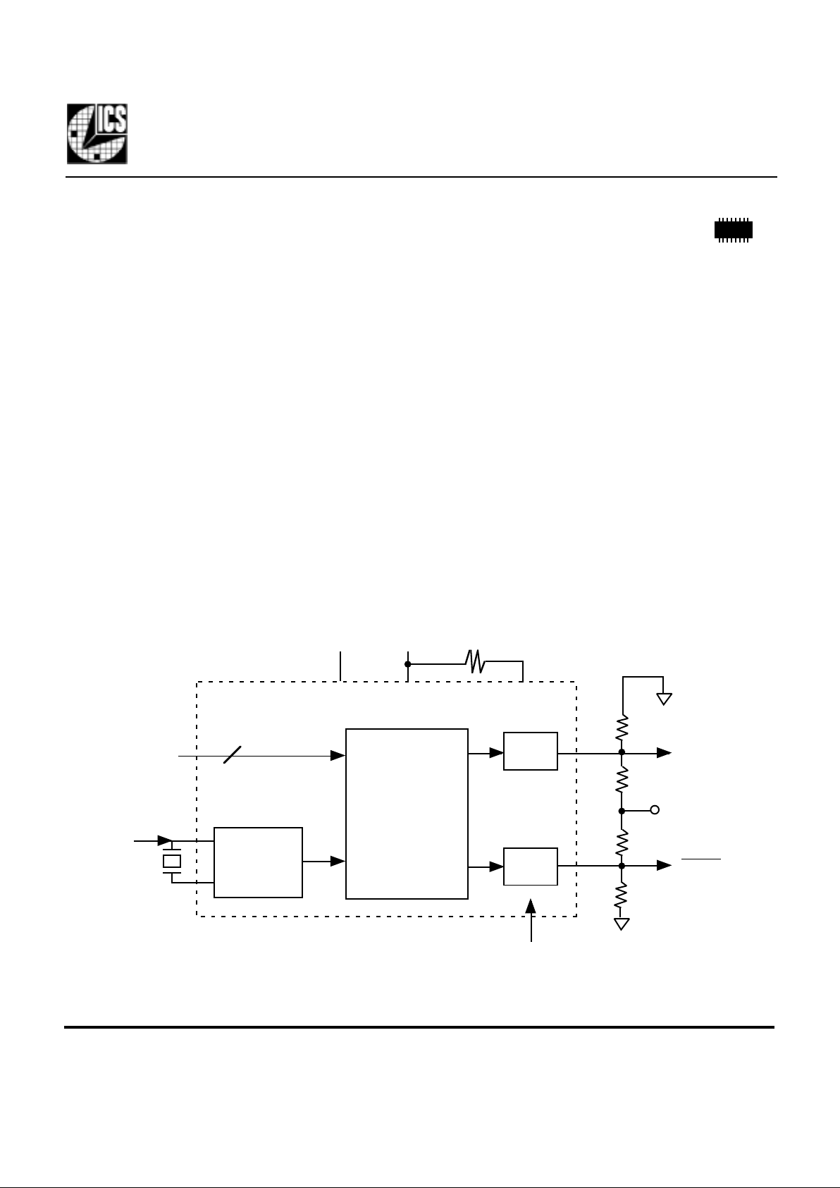
Block Diagram
GND
Crystal
or
clock
X1
X2
S0:1
Output
Buffer
Output
Buffer
PECL
PECL
62Ω
270Ω
270Ω
62Ω
VDD
RES
VDD
1.1kΩ
2
Output Enable
(both out
p
uts)
Output resistor values shown are for unterminated lines.
Refer to MAN09 for additional information.
Clock Synthesis
and Control
Circuitry
Clock
Buffer/
Crystal
Oscillator
Page 2
ICS507-01/02
PECL Clock Synthesizer
MDS 507 C 2Revision 042600 Printed 11/13/00
Integrated Circuit Systems, Inc. • 525 Race Street • San Jose •CA •95126• (408)295-9800tel • www.icst.com
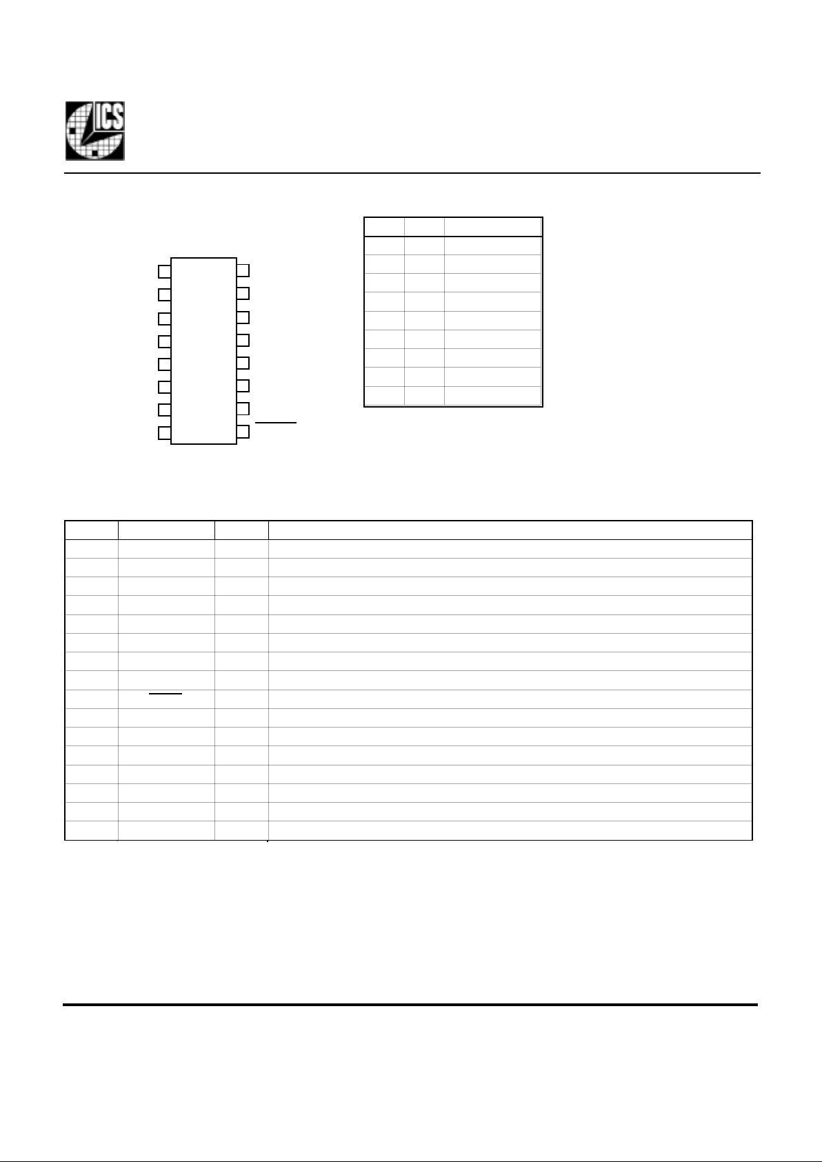
Pin Assignment
Pin Descriptions
Key: I=Input, O=output, TI=tri-level input, P=power supply connection; XI, XO=crystal connections
Clock Multiplier Select Table
16
15
14
13
16 pin narrow (150 mil) SOIC
12
11
10
9
1
2
3
4
5
6
7
8
ICS507-01/02
VDD
GND
X1/ICLK
VDD
S1
PECL
GND
NC
RES
NC
NC
X2
S0
OE
NC
0 = connect pin directly to ground
1 = connect pin directly to VDD
M = leave unconnected (floating)
PECL
S1 S0 Multiplier
0 0 9.72X*
0 M 10X
0 1 12X
M 0 6.25X
MM 8X
M1 5X
10 2X
1M 3X
11 4X
Number Name Type Description
1 X1/ICLK XI Crystal or clock connection. Connect to a fundamental parallel mode crystal, or clock.
2 VDD P VDD. Connect to +3.3 V or +5 V, and to VDD on pin 3.
3 VDD P VDD. Connect to VDD on pin 2. Decouple with pin 5.
4 S1 TI Multiplier select pin 1. Determines output frequency per table above.
5 GND P Connect to ground.
6 GND P Connect to ground.
7 NC - No connect. Nothing is connected internally to this pin.
8 PECL O PECL Output. Connect to resistor load as shown on page one.
9 PECL O Complementary PECL Output. Connect to resistor load as shown on page one.
10 RES I Bias Resistor Input. Connect a resistor between this pin and VDD.
11 NC - No connect. Nothing is connected internally to this pin.
12 NC - No connect. Nothing is connected internally to this pin.
13 OE I Output Enable. Tri-states both outputs when low. Internal pull-up.
14 S0 TI Multiplier select pin 0. Determines output frequency per table above.
15 NC - No Connect. Nothing is connected internally to this pin.
16 X2 XO Cr stal connection. Connect to cr stal, or leave unconnected for clock input.
*Use this selection to get
155.52 MHz from a 16 MHz
input.
For lowest phase noise
generation of 155.52 MHz,
use a 19.44 MHz crystal and
the 8X selection.
Page 3

ICS507-01/02
PECL Clock Synthesizer
MDS 507 C 3Revision 042600 Printed 11/13/00
Integrated Circuit Systems, Inc. • 525 Race Street • San Jose •CA •95126• (408)295-9800tel • www.icst.com
Parameter Conditions Minimum Typical Maximum Units
ABSOLUTE MAXIMUM RATINGS (stresses be ond these can permanentl damae the device)
Supply Voltage, VDD Referenced to GND 7 V
Inputs Referenced to GND -0.5 VDD+0.5 V
Clock Output Referenced to GND -0.5 VDD+0.5 V
Ambient Operating Temperatur
e ICS507M-0x 0 70 °C
ICS507M-0xI -40 85 °C
Soldering Temperature Max of 20 seconds 260 °C
Storage temperature -65 150 °C
DC CHARACTERISTICS (VDD = 5.0 V unless otherwise noted)
Operating Voltage, VDD 3.0 5.5 V
Input High Voltage, VIH ICLK only VDD/2 + 1 VDD/2 V
Input Low Voltage, VIL ICLK only VDD/2 VDD/2-1 V
Input High Voltage, VIH S0, S1 VDD-0.5 V
Input Low Voltage, VIL S0, S1 VDD+0.5 V
Output High Voltage, VOH Note 2 VDD-1.2 V
Output Low Voltage, VOL Note 2 VDD-2.0 V
IDD Operating Suppl Current, note 3 No Load, 155.52MHz 67 mA
Internal Cr stal Capacitance, X1 and X2 Pins 1, 8 26 pF
Input Capacitance S0, S1 4 pF
AC CHARACTERISTICS (VDD = 5.0 V unless otherwise noted)
Input Crystal Frequency 5 27 MHz
Input Clock Frequency 5 52 MHz
Output Frequency, ICS507-01 0 to 70°C VDD = 5.0 V 10 200 MHz
0 to 70°C VDD = 3.3 V 10 156 MHz
Output Frequency, ICS507-01I -40 to 85°C VDD = 3.3 V or 5.0 V 10 125 MHz
Output Frequency, ICS507-02I 0 to 70°C VDD = 5.0 V 125 200 MHz
0 to 70°C VDD = 3.3 V 125 200 MHz
-40 to 85°C VDD = 3.3 V or 5.0 V 125 160 MHz
Output Clock Duty Cycle 49 51 %
PLL Bandwidth 10 kHz
Absolute Clock Period Jitter Deviation from mean ±75 ps
One Sigma Clock Period Jitter 20 ps
Electrical Specifications
Notes: 1) All typical values are at 5.0 V and 25°C unless otherwise noted.
2) VOH and VOL can be set by the external resistor values on the PECL outputs.
3) IDD includes the current through the external resistors, which can be modified.
4) The phase relationship between input and output can change at power up. For a fixed phase relationship, see one of the
ICS zero delay buffers.
Page 4

ICS507-01/02
PECL Clock Synthesizer
MDS 507 C 4Revision 042600 Printed 11/13/00
Integrated Circuit Systems, Inc. • 525 Race Street • San Jose •CA •95126• (408)295-9800tel • www.icst.com
Applications
High Frequency Differential PECL Oscillators: The ICS507 plus a low frequency, fundamental mode
crystal can build a high frequency differential output oscillator. For example, a 10 MHz crystal connected
to the ICS507 with the 12X out
p
ut selected (S1=0, S0=1) produces a 120 MHz PECL output clock.
High Frequency VCXO: The bandwidth of the PLL is guaranteed to be greater than 10 kHz. This means
that the PLL will track any modulation on the input with a frequency of less than 10 kHz. By using this
property, a low frequency VCXO can be built, and the output can then be multiplied with the ICS507 to
g
ive a high frequency output, thereby producing a high frequency VCXO.
High Frequency TCXO: Extending the previous application, an inexpensive, low frequency TCXO can be
built and the output frequency can be multiplied using the ICS507. Since the output of the chip is phaselocked to the input, the ICS507 has no temperature dependence, and the temperature coefficient of the
combined system is the same as that of the low fre
q
uency TCXO.
Decoupling and External Components
The ICS507 requires a 0.01µF decoupling capacitor to be connected between VDD and GND on pins 2
and 5. It must be connected close to the ICS507. Other VDD and GND connections should be
connected to those pins, or to the VDD and GND planes on the board. A resistor must be connected
between the RES (pin 10) and VDD. Another four resistors are needed for the PECL outputs as shown on
the block diagram on page 1. Suggested values of these resistors are shown in the Block Diagram, but they
can be varied to chan
g
e the differential pair output swing, and the DC level; refer to MAN09.
Page 5

ICS507-01/02
PECL Clock Synthesizer
MDS 507 C 5Revision 042600 Printed 11/13/00
Integrated Circuit Systems, Inc. • 525 Race Street • San Jose •CA •95126• (408)295-9800tel • www.icst.com
While the information presented herein has been checked for both accuracy and reliability, Integrated Circuit Systems, Incorporated (ICS) assumes no responsibility for either its
use or for the infringement of any patents or other rights of third parties, which would result from its use. No other circuits, patents, or licenses are implied. This product is
intended for use in normal commercial applications. Any other applications such as those requiring extended temperature range, high reliability, or other extraordinary
environmental requirements are not recommended without additional processing by ICS. ICS reserves the right to change any circuitry or specifications without notice. ICS does
not authorize or warrant any ICS product for use in life support devices or critical medical instruments.
Ordering Information
Part/Order Number Marking Package Temperature Minimum
Quantities
ICS507M-01 ICS507M-01 16 pin narrow SOIC 0 to 70°C
-
ICS507M-01T ICS507M-01 16 pin SOIC on tape and reel 0 to 70°C 2500 pieces
ICS507M-01I ICS507M-01I 16 pin narrow SOIC -40 to 85°C
-
ICS507M-01IT ICS507M-01I 16 pin SOIC on tape and reel -40 to 85°C 2500 pieces
ICS507-01-DSW - Probed wafers, cut, on sticky tape 0 to 70°C 1 wafer
ICS507-01-DPK - Tested die in waffle pack 0 to 70°C 1000 pieces
ICS507-01-DWF - Die on uncut, probed wafers 0 to 70°C 1 wafer
ICS507M-02I ICS507M-02I 16 pin narrow SOIC -40 to 85°C
-
ICS507M-02IT ICS507M-02I 16 pin SOIC on tape and reel -40 to 85°C 2500 pieces
Package Outline and Package Dimensions
(
For current dimensional specifications, see JEDEC Publication No. 95.)
16 pin SOIC narrow
Inches Millimeters
Symbol Min Max Min Max
A 0.0532 0.0688 1.35 1.75
A1
0.0040 0.0098 0.10 0.24
B 0.0130 0.0200 0.33 0.51
C
0.0075 0.0098 0.19 0.24
D 0.3859 0.3937 9.80 10.00
E 0.1497 0.1574 3.80 4.00
e .050 BSC 1.27 BSC
H 0.2284 0.2440 5.80 6.20
h 0.0099 0.0195 0.25 0.50
L 0.0160 0.0500 0.41 1.27
B
D
EH
e
A1
C
A
h x 45°
L
INDEX
AREA
12
 Loading...