

Page 1
QTClock™ Quick Turn Clock Synthesizer
Description Features
ICS300/ICS301/ICS302
The ICS300 and ICS301 QTClocks™ generate a
high quality, high frequency clock output and a
reference from a low frequency crystal or clock
input. They are designed to replace crystals and
crystal oscillators in most electronic systems. The
ICS302 can accept a higher frequency clock input
to generate up to 200 MHz. The devices contain a
One Time Programmable (OTP) ROM which is
factory programmed with the PLL divider values
to output a broad range of frequencies, from 6 to
200 MHz, allowing customer requests for different
frequencies to be shipped in 1-3 days. Using
Phase-Locked-Loop (PLL) techniques, the devices
run from a standard fundamental mode,
inexpensive crystal, or clock. They are smaller and
less expensive than one oscillator.
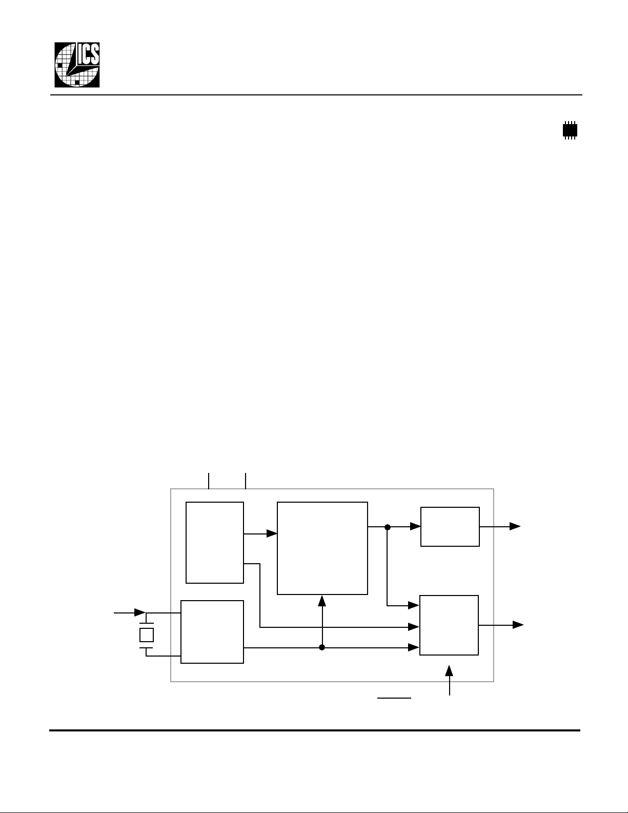
Block Diagram
VDD GND
• Packaged as 8 pin SOIC
• Quick turn frequency programming allows
samples in one to three days
• Replaces nearly any crystal or oscillator
• ICS300 produces up to 100 MHz at 3.3V,
ICS301 produces up to 200 MHz at 3.3V
ICS302 accepts up to 125 MHz clock input
• Easy to cascade with ICS5xx series
• Input crystal frequency of 5 - 27 MHz
• Input clock frequency of 2 - 125 MHz
• Low jitter - 50 ps one sigma
• Compatible with all popular CPUs
• Duty cycle of 45/55
• Operating voltages of 3.0 to 5.5V
• Full CMOS level outputs with 25mA drive
capability at TTL levels
• Tri-state output + PLL power down pin
• Advanced, low power CMOS process
Crystal
or clock
input
X1/ICLK
X2
OTP
ROM
with PLL
Divider
Values
Crystal
Oscillator
PLL
Clock
Synthesis
and Control
Circuitry
Output
Buffer
Divide
Logic and
Output
Buffer
CLK
REF
PDTS (both outputs and PLL)
MDS 300QT E 1 Revision 111000
Integrated Circuit Systems, Inc. • 525 Race Street • San Jose •CA•95126•(408) 295-9800tel• www.icst.com
Page 2
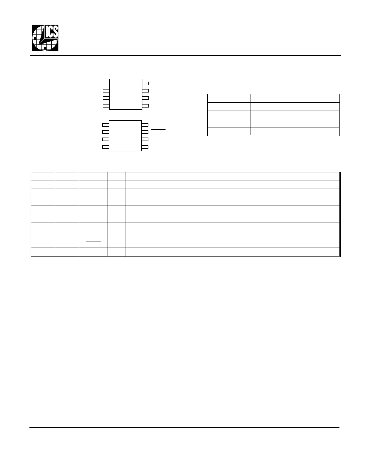
Pin Assignments
ICS300/ICS301/ICS302
QTClock™ Quick Turn Clock Synthesizer
X1/ICLK
VDD
GND
REF
GND
VDD
GND
REF
1
ICS300
2
ICS301
3
4
1
2
ICS302
3
4
8
X2
7
PDTS
6
DC
5
CLK
8
ICLK
7
PDTS
6
DC
5
CLK
REF Clock Options
REF Comments
Reference Buffered oscillator output
Reference/2 Oscillator frequency divided by two
CLK/2 CLK frequency divided by two
Off Output stopped low. Lowest jitter
Pin Descriptions
Number Number Name Type Description
300/1 302
1 8 X1/ICLK I Crystal connection or clock input. Clock only on ICS302.
2 2 VDD P Connect to +3.3V or +5V.
3 1, 3 GND P Connect to ground.
4 4 REF O Buffered crystal oscillator output clock, or variation per REF clock options table above.
5 5 CLK O Clock output. Fixed frequency between 6 and 200 MHz programmed at factory.
6 6 DC - Don't Connect anything to this pin.
7 7 PDTS I Powers down PLL, and puts both outputs into high impedance state, when low.
8 - X2 O Crystal connection. Leave unconnected for clock input.
Key: I = Input, O = output, P = power supply connection
Device Configuration
The specification is complete when the ICS300/301/302 QTClock Order Form accompanies this data
sheet. The order form lists the input, REF, and CLK actual frequencies, as well as any other available
options. This unique configuration is given a two character alphanumeric programming code, which must
be specified when referring to samples.
External Components / Crystal Selection
The ICS300/301/302 requires a 0.01µF decoupling capacitor to be connected between VDD and GND.
It must be connected close to the ICS300/301/302 to minimize lead inductance. No external power
supply filtering is required for this device. A 33Ω terminating resistor can be used next to the CLK and
REF pins. The total on-chip capacitance is approximately 16 pF, so a parallel resonant, fundamental mode
crystal should be used. For crystals with a specified load capacitance greater than 16 pF, crystal capacitors
can be connected from each of the pins X1 and X2 to Ground. The value (in pF) of these crystal caps
should be = (CL-16)*2, where CL is the crystal load capacitance in pF. These external capacitors are only
required for applications where the exact frequency is critical. For a clock input, connect to X1/ICLK and
leave X2 unconnected (no capacitors on either).
MDS 300QT E 2 Revision 111000
Integrated Circuit Systems, Inc. • 525 Race Street • San Jose •CA•95126•(408) 295-9800tel• www.icst.com
Page 3

ICS300/ICS301/ICS302
ABSOLUTE MAXIMUM RATINGS (stresses beyond these can permanently damage the device)
DC CHARACTERISTICS (VDD = 5.0V unless otherwise noted)
AC CHARACTERISTICS (VDD = 5.0V unless otherwise noted)
QTClock™ Quick Turn Clock Synthesizer
Electrical Specifications
Parameter Conditions Minimum Typical Maximum Units
Supply Voltage, VDD Referenced to GND 7 V
Inputs Referenced to GND -0.5 VDD+0.5 V
Clock Output Referenced to GND -0.5 VDD+0.5 V
Ambient Operating Temperature 0 70 °C
Soldering Temperature Max of 10 seconds 260 °C
Storage temperature -65 150 °C
Operating Voltage, VDD 3 5.5 V
Input High Voltage, VIH, ICLK only ICLK (Pin 1) (VDD/2)+1 VDD/2 V
Input Low Voltage, VIL, ICLK only ICLK (Pin 1) VDD/2 (VDD/2)-1 V
Input High Voltage, VIH PDTS 2 V
Input Low Voltage, VIL PDTS 0.4 V
Output High Voltage, VOH IOH=-4mA VDD-0.4 V
Output High Voltage, VOH IOH=-25mA 2.4 V
Output Low Voltage, VOL IOL=25mA 0.4 V
IDD Operating Supply Current, 20 MHz crystal No Load, 100MHz 20 mA
Short Circuit Current CLK output ±70 mA
On-Chip Pull-up Resistor, PDTS Pin 7 270 kΩ
Input Capacitance, PDTS Pin 7 4 pF
Input Frequency, crystal input, ICS300 and 301 5 27 MHz
Input Frequency, clock input, ICS300 and 301 2 50 MHz
Input Frequency, clock input, ICS302 50 125 MHz
Output Frequency, ICS300 VDD = 4.5 to 5.5V 6 160 MHz
Output Frequency, ICS300 VDD = 3.0 to 3.6V 6 100 MHz
Output Frequency, ICS301 and ICS302 VDD = 4.5 to 5.5V 6 200 MHz
Output Frequency, ICS301 and ICS302 VDD = 3.0 to 3.6V 6 200 MHz
Output Clock Rise Time 0.8 to 2.0V 1 ns
Output Clock Fall Time 2.0 to 0.8V 1 ns
Output Clock Duty Cycle (Note 1) at programmed level 45 49 to 51 55 %
Absolute Clock Period Jitter Deviation from mean ±120 ps
One Sigma Clock Period Jitter 50 ps
Power-up time, PDTS goes high until Refer. out Reference on REF clk 3 10 ms
Power-up time, PDTS goes high until CLK out 8 20 ms
Note 1: These are typical values. The actual minimum and maximum duty cycle limits are shown on the
ICS300/301/302 QTClock Order Form for each programmed version.
MDS 300QT E 3 Revision 111000
Integrated Circuit Systems, Inc. • 525 Race Street • San Jose •CA•95126•(408) 295-9800tel• www.icst.com
Page 4

ICS300/ICS301/ICS302
Inches
Millimeters
QTClock™ Quick Turn Clock Synthesizer
Package Outline and Package Dimensions
(For current dimensional specifications, see JEDEC Publication No. 95.)
8 pin SOIC
Symbol Min Max Min Max
A 0.0532 0.0688 1.35 1.75
A1
D 0.1890 0.1968 4.80 5.00
H 0.2284 0.2440 5.80 6.20
0.0040 0.0098 0.10 0.24
B 0.0130 0.0200 0.33 0.51
C
E 0.1497 0.1574 3.80 4.00
e
h 0.0099 0.0195 0.25 0.50
L 0.0160 0.0500 0.41 1.27
0.075 0.098 1.91 2.40
A1
Pin 1
e
D
E H
h x 45°
A
C
B
L
Ordering Information
Part/Order Number Marking Package Temperature
ICS300M-xx ICS300M 8 pin SOIC 0 to 70 °C
ICS300MT-xx ICS300M 8 pin SOIC on tape and reel 0 to 70 °C
ICS301M-xx ICS301M 8 pin SOIC 0 to 70 °C
ICS301MT-xx ICS301M 8 pin SOIC on tape and reel 0 to 70 °C
ICS302M-xx ICS302M 8 pin SOIC 0 to 70 °C
ICS302MT-xx ICS302M 8 pin SOIC on tape and reel 0 to 70 °C
xx represents a 2 character alphanumeric programming code assigned by the factory, which indicates the
output frequencies on CLK and REF. All samples are shipped with an ICS300/301/302 order form
describing the characteristics of the device.
While the information presented herein has been checked for both accuracy and reliability, Integrated Circuit Systems, Inc. (ICS) assumes no responsibility for either its use or for
the infringement of any patents or other rights of third parties, which would result from its use. No other circuits, patents, or licenses are implied. This product is intended for use
in normal commercial applications. Any other applications such as those requiring extended temperature range, high reliability, or other extraordinary environmental requirements
are not recommended without additional processing by ICS. ICS reserves the right to change any circuitry or specifications without notice. ICS does not authorize or warrant any
ICS product for use in life support devices or critical medical instruments.
MDS 300QT E 4 Revision 111000
QTClock is a trademark of ICS
Integrated Circuit Systems, Inc. • 525 Race Street • San Jose •CA•95126•(408) 295-9800tel• www.icst.com
 Loading...