

Page 1
Integrated
Circuit
Systems, Inc.
ICS1660
Incoming Call Line Identification (ICLID) Receiver
with R ing D etec tion
Features
•• Ring Dete c tio n
•• Low Battery Detection
•• Internal 5V Regulator - can externally source 25mA
•• FSK Demodulat ion
•• Power-down in Standby Mode
•• Direct Interfac e to Host Micropr oc essor or
Microcomputer
Applications
•• Telephones
•• Facsimile Ma chines
•• Modems
•• Telephon e Interface Equipm e nt
•• Stand-a lon e ICLI D produ ct s
Description
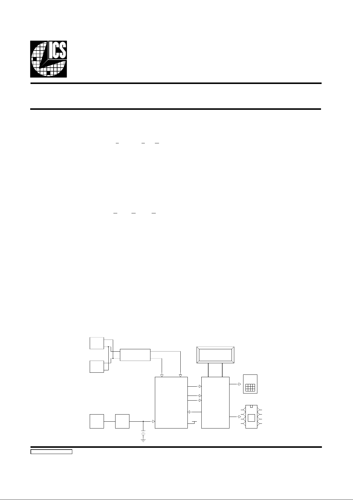
The ICS1660 “ICLID” circuit is a monolithic CMOS VLSI
device that decodes and detects the
Frequency Shift Keying
(FSK) signals used in caller identification telephone service.
The ICS1660, when used in conjunction with some external
components, amplifies, filters and demodulates the FSK
data transmitted from the central office to the telephone
subscriber .
The ICS1660 detects the first power ring signal and demodulates the 1200 baud FSK data transmitted during the silent
interval between the first and second powe r ring. The FSK data
is transmitted from the central office switch to the subscriber
line as part of the CLASS se rvi ce of
Calling Number Delivery
(CND). This data is then demodulated, amplified and filtered
by the ICS1660 and digitally transmitted to the host controller/processor.
The ICS1660 is designed to be powered by any off-the-shelf
9.0 volt battery. Th e on-ch ip 5.0 vol ta ge regula t or powe rs the
host microprocessor and any external circuitry supported by
the ICS1660. This portion of th e circuit ca n be overri dden by
connecti ng the V
IN
pin (18) to the VDD pin (1) for a common
power supply. A low ba t te ry d ete ct ion c ircui t is al so pr ovi de d
on-chip and signals the microprocessor on the FSK/BAT pin
(17) when the PW R pin (16) i nput is pulle d lo w.
TO LINE
TO PHONE
Surge and
Lightning
Protection
2 x 16 LCD
Display
AC/DC
Adapter
DC
Jack
KEYPAD
External
Memory
(RAM/EPROM)
8
Data
3
Control
ICS1660
Rng Detect
FSK Demodulation
Signal Conditioning
Low Battery Detect
Power-down
Standby
Voltage
Regulation
9VDC
+5VDC
Micro-
Controller
ICLID Block Diagram
ICS1660RevA100694
Page 2
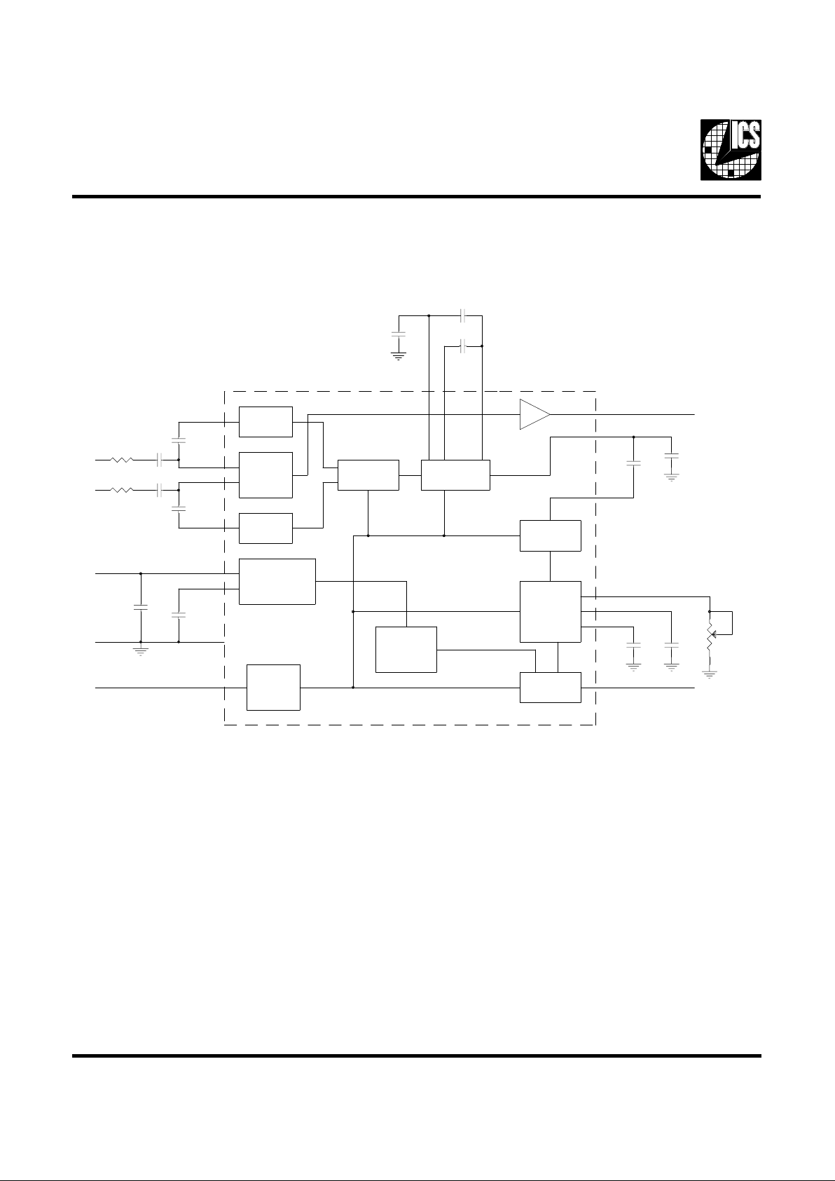
Block Diagram
.022µF
F1 F2 F3
.033µF
RING
FOUT
.0033µF
.022µF
AMPIN
VCOSET
LFILTER
POSTF
500k.01µF
1000pF
FSKBAT
MUX
PLL
LOW
BATTERY
DETECT
POST
AMP
POWER
CONTROL
REGULATOR
5 VOLT
BUFFER
RING
DETECT
DIFF
AMP
FILTER
PWR
10
µF
VIN
VDD
VSS
BUFFER
0.01
µF
0.01µF
LINE AF
LINE BF
LINE A
LINE B
82k
0.1µF
0.1µF
82k
TIP
RING
15 10 13 2
11
12
6
4
3
17
16
9
18
1
14
8
7
5
ICS1660
2
Page 3

Function Description
Power Supply
The ICS1660 is desig ned to be power ed by a standard 9.0 volt
battery. The chip contains a voltage regulator that powers
extern al circ uitry and pro vides t he suppl y vol tage fo r all digital
I/O on the circuit. This allows easy interface between the
ICS1660 and othe r standa rd log ic worki ng at 5.0 V. Thi s regu lator has short circuit protection and requires an external filter/compe nsat io n capa c itor with a minimum val ue of 10uf.
In the event that an external regulated 5.0V supply is available,
the V
IN
and VDD pins can be shorte d to permit the entire system
to work from a common supply .
A low battery detection circuit is provided. This circuit is
designed for a typical tri p point of 6.0 V with hysteresi s of about
200mV above the trip point. This signal is low active and is
multiplexed to the FSKBAT output pin when the PWR input is
low.
In an effort to keep powe r dissipati on to a minimum and ext end
batte ry life , most of the an alog c ircui ts are tu rned off when the
circuit is at rest waiting for a ring detect, (PWR pin low).
During this time only the regulator, low battery detect, reference generator, and ring detect circuits are active. When the
PWR pin is high, all circuits are active.
Ring Detect
As shown in the attached block diagram, the LINEA and
LINEB inputs should be connected to the telephone line
through external 82kΩ resistors and 0.1uf capacitors. This
provides DC i sola t ion an d set s up a voltage di vid er wit h i nt er nal resistors t hat will detec t 35.0V RMS typica lly. This vol tage
is applied across the LINEA and LINEB inputs. The design
value of the internal resistors is 8.1KΩ ± 20% with relative
accuracy of 2%. The RING output is high active.
Differential Front End
As shown in the attached block diagram, the LINEA and
LINEB inputs go into a differential amplifier which in turn
drives a filter. All resistors are internal to the chip while
capacitors are connec t ed as shown in the bl ock diagram. After
filtering, the signal is AC coupled into a high gain amplifier
that conv erts the signal t o digital. This di gital si gnal i n turn a cts
as the reference frequency for the phase comparator section of
the phase locked loop.
FSK Demodulation
After the signal from the telephone line has been filtered,
amplifie d a nd co nve rt ed to dig it al, it a cts as an input t o a ph ase
locked l oop. This PLL does FSK demo dulation . The summ ing
amplifier shown in the block diagram provides a signal to the
VCO that should be about 0.5V for MARK frequency
(1200 HZ), and 2.0V for SPACE fre que nc y (2 200 HZ ).
As shown in the block diagram, the LFILTER (loop filter)
output has a post filter att ached to it. This POSTF signa l is sent
to a comparator. The other side of the comparator is set to
approximately 2.5V. This comparator has a small amount
(200mV) of hysteresis and its output is the demodulated FSK
data. The FSK output is high for MARK freq uency and low for
SPACE frequency. FSK data is multiplexed out of the
FSKBAT pin when the PWR input is high.
The VCO frequency is set with one external resistor with a
value in t he range of 3 00K fo r a cent e r fre qu ency of 1700 HZ.
The lock r an ge wil l be 66 0 HZ to 2630 HZ t ypi cal . Th e ce nt e r
frequen cy reproduc i bil it y wil l be ±1 5 %. Th e c e nte r frequency
can be adjusted in the system by connecting AMPIN to VSS,
PWR to VDD, and ad justing the exter nal resist or for 17 00 HZ.
This freque nc y can be observed at the LFILTE R outp ut or the
FSK/BAT output.
ICS1660
3
Page 4

Typical Application
120VAC
AC/DC
ADAPTER
12VDC
1N4002 x 4
300
9.1V
1N4002
9 V
DC
0.1µF
100µF
.022µF
.033µF
.033µF
0.01µF
1000 pF
VR1
18
VIN
4
LFILTER
6
VCOSET
3
POSTF
13
10
FILTER2
15
FILTER1
14
LINE BF
8
LINE B
0.01µF
250V
TIP
RING
10 OHM
MOV
82k 82k
0.1µF
250V
0.1
µF
250V
0.01
µF
250V
+5V
A B
7
LINE A
5
LINE AF
16
PWR
17
FSK/BAT
2
RING
FILTER
OUT
11
12
AMP IN
1
VDD
100
µF
0.1
µF
A B
0.0033µF
TP1
TP2
0.022µF
VOUT
MICRO
CONTROLLER
9
VSS
CAL JUMPER
5V
+/− 10%
CAL JUMPER
ICS1660
ICS1660
4
Page 5

Pin Descriptions
PIN NUMBER NAME DESCRIPTION
DIP SO
1 1 VDD Supply vol ta ge pin to ext er na l circ ui ts. Outpu t of 5.0 vo lt reg ula t or.
2 2 RING Ring detect output signal to the host mic ropr ocessor.
3 3 POSTF Post lo op filt er signa l used by dem odu lato r.
4 4 LFI LT E R Loop filt er for PLL.
5 5 LINEAFILTER Filter input from line “A.”
6 6 VCOSET Center freque nc y adjust ment pin .
7 7 LINEA “Tip” input from telephon e line.
8 8 LINEB “Ring” input from telep hone line.
9 9 VSS Ground.
10 11 FILTER2 Activ e filte r pin .
11 12 FILTEROUT Active filter pin .
12 13 AMPIN Input from active filter.
13 14 FILTER3 Activ e filte r pin .
14 15 LINEBFIL TE R Filter input from line “B.”
15 16 FILTER1 Activ e filte r pin .
16 17 PWR Logic in put signa l to switch fr om low curre nt standby mod e.
17 18 FSK/BAT Multiplexe d output signal controlled by PWR pin. In standb y mo de , this is a
low battery (active low) signal. During FSK demodulatio n, this is the data lin e
to the µP (ma rk = high ).
18 19 VIN Input power supply pin.
10 20 NC on SOIC
ICS1660
5
Page 6

Input/Output Specifications
Digital
RING and FSKBAT outputs are standard CMOS outputs with
voltage swings between V
SS
and VDD.
PWR is a logic input. A level converter circuit is on chip to
allow the logic signal that swing between V
SS
and VDD to be
internally converted to signals that swing between V
SS
and
V
IN
. It should be noted that to minimize power consumption
caused b y throug h curre nt in logic ga tes, the PW R inp ut shoul d
always swing to within 100 mV of V
SS
or VDD. The PWR
input signa l is lo w whe n t he ICS1660 is in lower p owe r mode
waiting for a n inc om i ng c al l.
The LFIL TER outpu t is a sta ndard C MOS output powered from
VDD. This output has an interna l resistor wi th a typic al value
of 30kΩ. This is u sed in conju nction wi th th e exte rnal ca pacito r
shown in the block diagram t o form the loop fi lter for the PLL.
Analog
The value of the ring detect is as previously discussed 35.0V
RMS typical. The actual value is set by the choice of the
external resist ors that are connec ted to the LINEA and LINE B
inputs. The matching of these resistors to the internal 8.1kΩ
resistors is also a factor. The signal level at the chip that will
cause a ring is the bandgap voltage, (1.25V) or below.
The chip is designed for an input signal level of -12.5dbm to
-28.5dbm into 900 ohms. This translates to a signal that is
between 100 mV and 636 mV peak to peak.
The filter section should be connected as shown in the block
diagram. Using the externa l capacitors as shown, and assuming
nominal val ues on the int erna l resistors, the corne r fre quenc ies
are 900 HZ and 3860 HZ.
An external resistor with a value of approximately 330kΩ is
connected b etwe en the LFIL T ER an d POSTF pads. Thi s re sistor along with the external capacitor shown in the block diagram form th e post fil ter. T his post fi lter is used in c on junct ion
with the compa rato r to do the FSK dem od ulat ion .
Absolute Maximum Ratings*
(Voltages refe re nc ed to VSS)
Supply Voltage . . . . . . . . V
IN
. . . . . . . . . -0.5V to +10V
Voltage at an y Input . . . . . . . . . . . . . . . . . -0.5V to V
DD
+ 0.5V
Operation Temperature Range . . . . . . . . . . . -55°C to +125°C
Storage Temperature Range . . . . . . . . . . . . . -50°C to 150 °C
* Absolute maxi m um rat ings are th ose val ue s beyo nd whi ch the safet y of th is devic e cann ot be guara nt e ed .
These values are NOT RE COMME NDED op erat ing conditions.
ICS1660
6
Page 7

DC Characteristics
VIN = 4.5V - 10 .0V; TA = 0 °C - 70 °C, Recommended Operating Range
PARAMETER SYMBOL CONDITIONS MIN TYP MAX UNITS
Standby Curren t I
IN
PWR LOW, VIN =9.0V,
I
DD
=2µA
-2030uA
Active Cu rre nt I
IN
PWR HIGH, VIN=9.0V
VCOSET=300k
- - 10 mA
Regulat or Out put Volt a ge V
DD
4.5 5.0 5.5 Volts
Regulator Out put Curr en t I
DD
Output Current 2.0 25.0 mA
Regulat or Dropout V
IN
0.5 1.0 Volts
Low Battery Detect 6.0 Volts
Low Battery Detect
Hysteresis
Low Battery Detect - Hysteresis 200 mV
OUTPUT CURRENT SINK/SOURCE
Ring Source Curren t I
OUT
VOUTH = VDD - 0.5V -5 0 0 - - uA
FSKBAT and Ring Sink
Current
I
OUT
VOUTL = VSS + 0.4V - - 500 uA
Ordering Information
ICS1660N or ICS1660M
Example:
ICS XXXX M
Package Type
N=DIP (Plastic)
M=SOIC
Device Type (cons ists of 3 or 4 digit numbe rs )
Prefix
ICS, AV=Standard Device; GSP=Genlock Device
ICS1660
7
 Loading...