

Page 1
7/12/00
ICPL2530, ICPL2531
HIGH SPEED DUAL CHANNEL
OPTICALLY COUPLED ISOLATOR
PHOTOTRANSISTOR OUTPUT
APPROVALS
l UL recognised, File No. E91231
DESCRIPTION
These dual channel diode-transistor optocouplers
use a light emitting diode and an integrated photon
detector to provide 2500Volts
between input and output. Seperate connection for
electrical isolation
RMS
the photodiode bias and output transistor collector
improve the speed up to a hundred times that of a
conventional photo-transistor coupler by reducing
the base-collector capacitance.
FEATURES
l High speed - 1 MBits/s
l High Common Mode Transient
Immunity 1000V/µs
l TTL Compatible
l 3 MHz Bandwidth
l Open Collector Outputs
l 2500V
l ICPL2531 has improved noise shield
Withstand Test Voltage,1 Min
RMS
which gives superior common mode
rejection
l Options :-
10mm lead spread - add G after part no.
Surface mount - add SM after part no.
Tape&reel - add SMT&R after part no.
l All electrical parameters 100% tested
l Custom electrical selections available
APPLICATIONS
l Line receivers
l Pulse transformer replacement
l Wide bandwidth analog coupling
l Output interface to CMOS-LSTTL-TTL
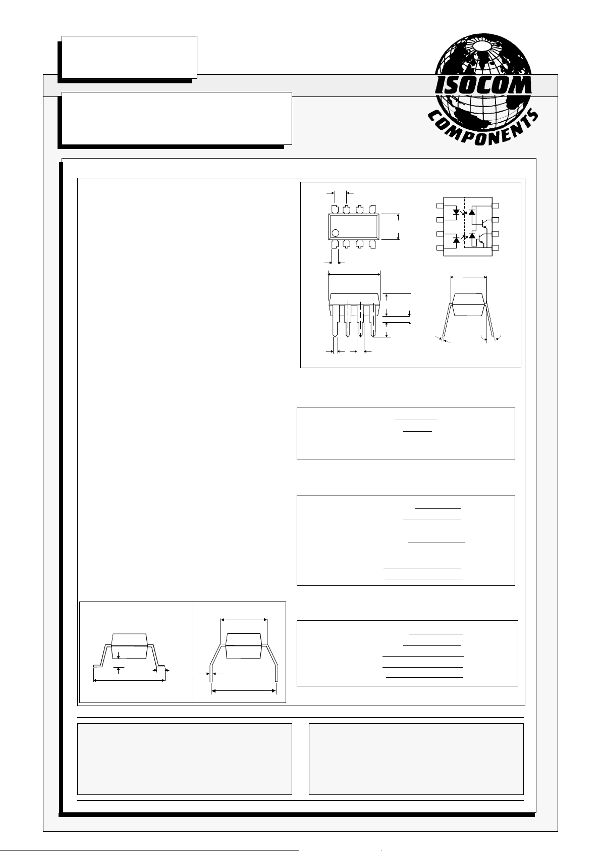
Dimensions in mm
1
2
3
4
* ICPL2531 NOISE SHIELD
*
7.62
8
7
6
5
1.3
2.54
6.9
6.3
9.7
9.1
4.0
3.6
0.5
1.3
3.3
0.5
0.3
15°
Max
ABSOLUTE MAXIMUM RATINGS
(25°C unless otherwise specified)
Storage Temperature -55°C to + 125°C
Operating Temperature -55°C to + 100°C
Lead Soldering Temperature
(1/16 inch (1.6mm) from case for 10 secs) 260°C
INPUT DIODE
Average Forward Current 25mA ( 1 )
Peak Forward Current 50mA ( 2 )
( 50% duty cycle, 1ms pulse width )
Peak Transient Current 1.0A
(equal to or less than 1µs P.W., 300 pps)
Reverse Voltage 5V
Power Dissipation 45mW( 3 )
OPTION GOPTION SM
SURFACE MOUNT
1.2
0.6
1.4
0.9
7.62
0.3
10.2
9.5
10.16
ISOCOM COMPONENTS LTD
Unit 25B, Park View Road West,
Park View Industrial Estate, Brenda Road
Hartlepool, Cleveland, TS25 1YD
Tel: (01429) 863609 Fax :(01429) 863581
DETECTOR
Average Output Current 8mA
Peak Output Current 16mA
Supply Voltage -0.5 to +30V
Output Voltage -0.5 to +20V
Power Dissipation 35mW( 4 )
ISOCOM INC
1024 S. Greenville Ave, Suite 240,
Allen, TX 75002 USA
Tel: (214) 495-0755 Fax: (214) 495-0901
e-mail info@isocom.com
http://www.isocom.com
DB92030-AAS/A3
Page 2

7/12/00
ELECTRICAL CHARACTERISTICS ( TA= 0°C to 70°C Unless otherwise noted )
PARAMETER SYM DEVICE MIN TYP* MAX UNITS TEST CONDITION
ICPL2530 7 18 % IF = 16mA, VO = 0.5V
Current Transfer Ratio CTR ICPL2531 19 % VCC = 4.5V, TA= 25°C
(note 5,6 )
ICPL2530 5 13 % IF = 16mA, VO = 0.5V
ICPL2531 15 % VCC = 4.5V
ICPL2530 0.1 0.5 V IF = 16mA, IO=1.1mA
Logic Low Output Voltage V
(note 5 )
OL
V
= 4.5V, TA= 25°C
CC
ICPL2531 0.1 0.5 V IF = 16mA, IO=2.4mA
V
= 4.5V, TA= 25°C
CC
Logic High Output Current I
(note 5 ) V
Logic Low Supply Current I
Logic High Supply Current I
OH
CCL
CCH
Input Forward Voltage V
(note 5 )
Temperature Coefficient
of Forward Voltage ∆V
(note 5 ) ∆T
Input Reverse Voltage V
(note 5)
Input Capacitance C
(note 5 )
0.02 500 nA I
0.01 10 µA I
= IF2= 0mA,TA= 25°C
F1
= V
= V
= V
= 5.5V
CC
= 15V
CC
O1
= IF2= 0mA
F1
V
= V
O1
O2
O2
80 µA IF1= IF2=16mA,VCC=15V
V
= V
O1
= open
O2
0.01 4 µA IF1= IF2= 0mA,VCC=15V
V
= VO2 = open
O1
F
F
A
R
IN
1.5 1.7 V IF = 16mA, TA= 25°C
-1.6 mV/°C IF = 16mA
5 V IR = 10µA,TA= 25°C
60 pF f = 1MHz, VF = 0
Input-output Isolation Voltage V
(note 7) 50%, t = 1min. TA= 25°C
Resistance (Input to Output) R
(note 7)
Capacitance (Input to Output) C
(note 7)
Input-Input Insulation I
Leakage Current (note 8) t = 5s, V
Resistance (Input to Input)(note8) R
Capacitance (Input to Input)(note8) C
ISO
IO
IO
I-I
I-I
I-I
2500 5000 V
12
10
RMS
Ω V
R.H.equal to or less than
= 500V dc
IO
0.6 pF f = 1MHz
0.005 µA 45 % Relative Humidity
11
10
Ω V
= 500V dc
I-I
0.25 pF f = 1MHz
* All typicals at TA= 25°C
= 500V dc
I-I
DB92030-AAS/A3
Page 3

SWITCHING SPECIFICATIONS AT TA = 25°C ( VCC = 5V, IF = 16mA Unless otherwise noted )
7/12/00
PARAMETER SYM DEVICE MIN TYP MAX UNITS TEST CONDITION
Propagation Delay Time t
ICPL2530 0.5 1.5 µs RL= 4.1kΩ,(note11 )
PHL
to Logic Low at Output ( fig 1 ) ICPL2531 0.2 0.8 µs RL= 1.9kΩ,(note10 )
Propagation Delay Time t
ICPL2530 0.5 1.5 µs RL= 4.1kΩ,(note11 )
PLH
to Logic High at Output ( fig 1 ) ICPL2531 0.2 0.8 µs RL= 1.9kΩ,(note10 )
Common Mode Transient ICPL2530 1000 V/µs IF = 0mA, V
Immunity at Logic High RL= 4.1kΩ,(note9,11 )
Level Output ( fig 2 ) CM
H
ICPL2531 1000 V/µs IF = 0mA, V
RL = 1.9kΩ,(note9,10 )
Common Mode Transient ICPL2530 -1000 V/µs V
Immunity at Logic Low RL = 4.1kΩ,(note9,11 )
Level Output ( fig 2 ) CM
L
ICPL2531 -1000 V/µs V
= 10V
CM
= 10V
CM
RL = 1.9kΩ,(note9,10 )
PP
PP
CM
CM
= 10V
= 10V
Bandwidth BW 3 MHz RL = 100Ω, (note 12 )
NOTES:-
1. Derate linearly above 70oC free air temperature at a rate of 0.8 mA/°C.
2. Derate linearly above 70oC free air temperature at a rate of 1.6 mA/°C.
3. Derate linearly above 70oC free air temperature at a rate of 0.9 mW/°C.
4. Derate linearly above 70oC free air temperature at a rate of 1.0 mW/°C.
5. Each channel .
6. CURRENT TRANSFER RATIO is defined as the ratio of output collector current,IO , to the forward LED
input current, IF times 100%.
7. Device considered a two-terminal device: pins 1,2,3, and 4 shorted together and pins 5,6,7 and 8 shorted
together.
8. Measured between pins 1 and 2 shorted together, and pins 3 and 4 shorted together.
9. Common mode transient immunity in Logic High level is the maximum tolerable (positive) dVcm/dt on
the leading edge of the common mode pulse VCM to assure that the output will remain in a Logic High
state (i.e. VO > 2.0V). Common mode transient immunity in Logic Low level is the maximum tolerable
(negative) dVcm/dt on the trailing edge of the common mode pulse signal, VCM to assure that the output
will remain in Logic Low state (i.e. VO< 0.8V).
10. The 1.9kΩ load represents 1 TTL unit load of 1.6mA and the 5.6kΩ pull-up resistor.
11. The 4.1kΩ load represents 1 LSTTL unit load of 0.36mA and the 6.1kΩ pull-up resistor.
12. The frequency at which the a.c. output voltage is 3dB below the low frequency asymptote.
PP
PP
FIG.1 SWITCHING TEST CIRCUIT
PULSE
GENERATOR
ZO = 50Ω
I
F
0
V
O
1.5V
t
PHL
t
PLH
1.5V
5V
V
OL
tr = 5ns
10% Duty Cycle
1/f < 100µs
IF Monitor
I
F
100Ω
1
2
3
4
8
7
5V
R
L
V
O
6
5
CL = 15pF
DB92030-AAS/A3
Page 4

7/12/00
FIG. 2 TEST CIRCUIT FOR TRANSIENT IMMUNITY AND TYPICAL WAVEFORMS
V
CM
10V
90%
10%
0V
V
O
t
r
SWITCH AT A: IF = 0mA
V
O
SWITCH AT B: IF = 16mA
Normalized Current Transfer
Ratio vs. Forward Current
1.6
1.5
1.4
1.3
1.2
1.1
1
I
F
10%
90%
t
f
5V
V
OL
A
B
V
FF
2
3
4
V
+
8
7
6
5
CM
-
5V
R
L
V
O
PULSE GEN.
Logic High Output Current vs.
Ambient Temperature
1
10
(nA)
OH
10
10
0
-1
IF = 0mA
VO = VCC = 5V
1.0
0.9
0.8
0.7
Normalized current transfer ratio
Normalized
to IF = 16mA
VO = 0.4V
VCC = 5V
TA = 25°C
1 2 5 10 20 50
Forward current IF (mA)
Normalized Current Transfer
Ratio vs. Ambient Temperature
1.3
1.2
1.1
1.0
0.9
0.8
0.7
Normalized current transfer ratio
Normalized
to IF = 16mA
VO = 0.4V
VCC = 5V
TA = 25°C
-2
10
Logic high output current I
-3
10
-55 -25 0 25 50 75 100
Ambient temperature TA ( °C )
Normalized Propagation Delay
vs. Ambient Temperature
1.5
1.4
1.3
t
PLH
t
PHL
1.2
1.1
1.0
0.9
Normalized
to IF = 16mA
0.8
Normalized propagation delay
0.7
VCC = 5V
RL = 4.1kΩ
TA = 25°C
-55 -25 0 25 50 75 100
Ambient temperature TA ( °C )
-25 0 25 50 70
Ambient temperature TA ( °C )
DB92030-AAS/A3
 Loading...