

Page 1
ICM7224
August 1997
Features
• High Frequency Counting - Guaranteed 15MHz, Typically
25MHz at 5V
• Low Power Operation - Typically Less Than 100µW
Quiescent
•
STORE and RESET Inputs Permit Operation as
Frequency or Period Counter
• True
•
COUNT INHIBIT Disables First Counter Stage
CARRY Output for Cascading Four-Digit Blocks
• Schmitt-Trigger on the COUNT Input Allows Operation
in Noisy Environments or with Slowly Changing Inputs
• Leading Zero Blanking INput and OUTput for Correct
Leading Zero Blanking with Cascaded Devices
• Provides Complete Onboard Oscillator and Divider
Chain to Generate Backplane Frequency, or
Backplane Driver May be Disabled Allowing Segments
to be Slaved to a Master Backplane Signal
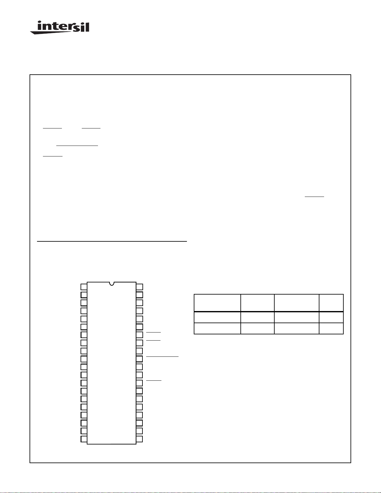
Pinout
ICM7224
(PDIP)
TOP VIEW
41/2 Digit LCD Display Counter
Description
The ICM7224 device is a high-performance, CMOS 41/
digit counter, including decoder, output latch, display driver,
count inhibit, leading zero blanking, and reset circuitry.
The counter section provides direct static counting, guaranteed from DC to 15MHz, using a 5V ±10% supply over the
operating temperature range. At normal ambient temperatures, the devices will typically count up to 25MHz. The
COUNT input is provided with a Schmitt trigger to allow
operation in noisy environments and correct counting with
slowly changing inputs. The COUNT INHIBIT, STORE and
RESET inputs allow a direct interface with the ICM7207 and
ICM7207A to implement a low cost, low power frequency
counter with a minimum component count.
These devices also incorporate several features intended to
simplify cascading four-digit blocks. The
allows the counter to be cascaded, while the Leading Zero
Blanking INput and OUTput allows correct Leading Zero
Blanking between four-decade blocks. The BackPlane driver
of the LCD devices may be disabled, allowing the segments
to be slaved to another backplane signal, necessary when
using an eight or twelve digit, single backplane display.
These devices provide maximum count of 19999. The
display drivers are not of the multiplexed type and each display segment has its own individual drive pin, providing high
quality display outputs.
CARRY output
2
1
V
DD
2
E1
3
G1
F1
4
5
BP
A2
6
7
B2
8
C2
D2
9
10
E2
G2
11
12
F2
A3
13
B3
14
15
C3
D3
16
17
E3
G3
18
F3
19
20
A4
40
D1
39
C1
38
B1
37
A1
36
OSCILLATOR
35
V
SS
STORE
34
RESET
33
COUNT
32
COUNT INHIBIT
31
LZB OUT
30
LZB IN
29
CARRY
28
1
/2 - DIGIT
27
F4
26
G4
25
E4
24
D4
23
C4
22
B4
21
Ordering Information
TEMP.
PART NUMBER
ICM7224IPL -25 to 85 40 Ld PDIP E40.6
ICM7224RIPL † -25 to 85 40 Ld PDIP E40.6
RANGE (oC) PACKAGE
† “R” Indicates Device With Reversed Leads Configuration.
PKG.
NO.
CAUTION: These devices are sensitive to electrostatic discharge; follow proper IC Handling Procedures.
http://www.intersil.com or 407-727-9207
| Copyright © Intersil Corporation 1999
9-14
File Number 3168.1
Page 2
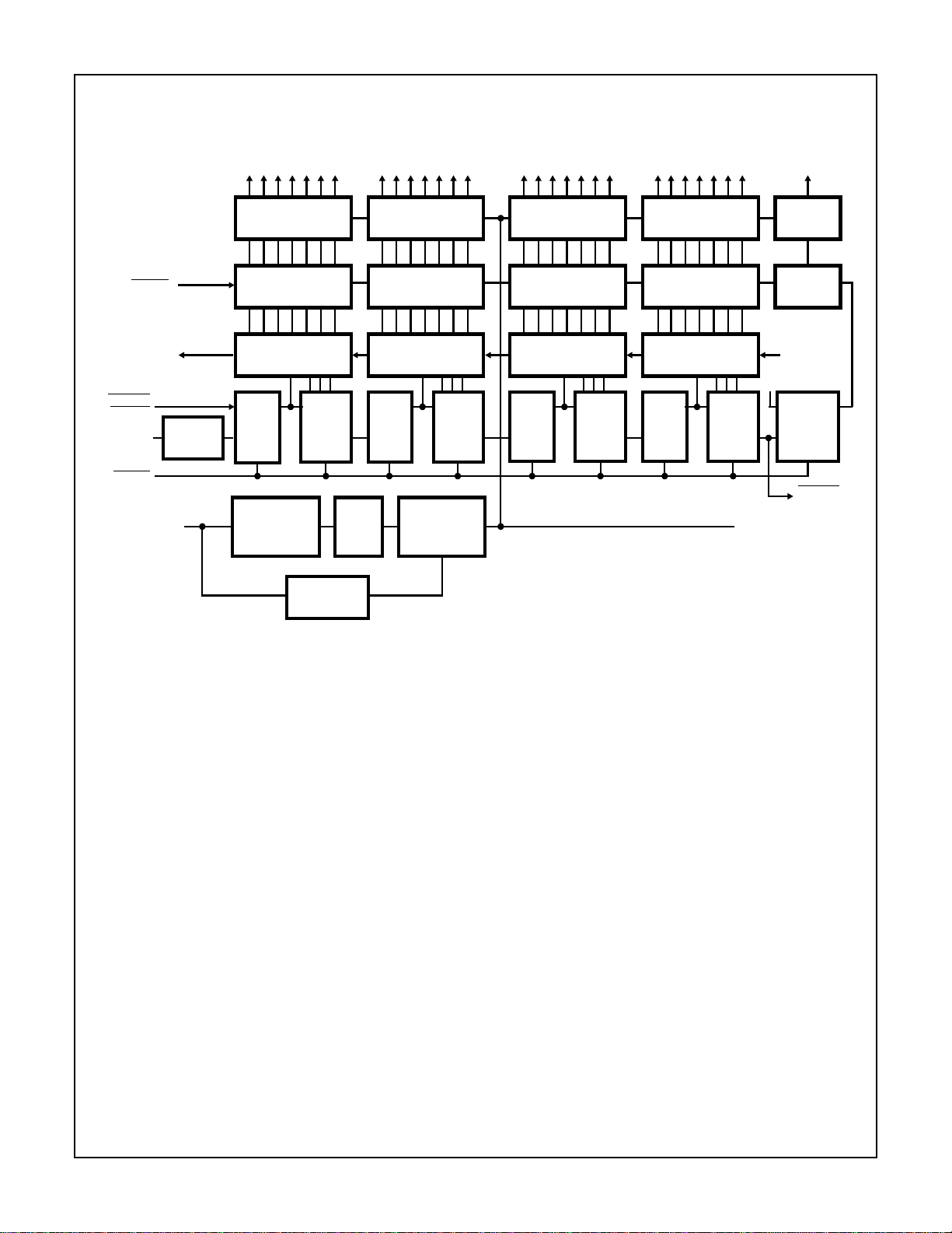
Functional Block Diagram
ICM7224
STORE
LEADING
ZERO
BLANKING
OUTPUT
COUNT
INHIBIT
COUNT
INPUT
RESET
OSCILLATOR
INPUT
SCHMITT
TRIGGER
LSD
DIGIT 1
SEGMENT OUTPUTS
7 WIDE DRIVER
7 WIDE LATCH
DECODER
CL
Q
2
÷
CL
R
OSCILLATOR
5
÷
Q
R
ENABLE
DETECTOR
DIGIT 2
SEGMENT OUTPUTS
7 WIDE DRIVER
7 WIDE LATCH
DECODER DECODER DECODER
Q
2
÷
CL
R
BLACKPLANE
+124
CL
÷
DRIVER
ENABLE
MSD
1
V
DD
D
CL
/2 DIGIT
OUTPUT
1
/2 DIGIT
DRIVER
1
/2 DIGIT
LATCH
LEADING
ZERO
BLANKING
INPUT
Q
1
/
2
DIGIT
R
CARRY
OUTPUT
DIGIT 3
SEGMENT OUTPUTS
7 WIDE DRIVER
7 WIDE LATCH
CL
Q
5
Q
R
CL
2
÷
R
5
÷
Q
R
DIGIT 4
SEGMENT OUTPUTS
7 WIDE DRIVER
7 WIDE LATCH
CL
Q
CL
2
÷
R
5
÷
Q
R
BP INPUT/OUTPUT
9-15
Page 3
ICM7224
Absolute Maximum Ratings Thermal Information
Supply Voltage (VDD - VSS). . . . . . . . . . . . . . . . . . . . . . . . . . . .6.5V
Input Voltage (An y Terminal) (Note 1). . . .(VDD+ 0.3V) to (VSS- 0.3V)
Operating Conditions
Temperature Range . . . . . . . . . . . . . . . . . . . . . . . . . . -25oC to 85oC
CAUTION: Stresses above those listed in “Absolute Maximum Ratings” may cause permanent damage to the device. This is a stress only rating and operation
of the device at these or any other conditions above those indicated in the operational sections of this specification is not implied.
NOTES:
1. Due to the SCR structure inherent in the CMOS process, connecting any terminal to voltages greater than VDD or less than VSS may
cause destructive device latchup. For this reason, it is recommended that no inputs from sources operating on a different power supply
be applied to the device before its supply is established, and that in m ultiple supply systems, the supply to the ICM7224 be turned on first.
2. θJA is measured with the component mounted on an evaluation PC board in free air.
Thermal Resistance (Typical, Note 2) θJA (oC/W)
PDIP Package. . . . . . . . . . . . . . . . . . . . . . . . . . . . . 50
Maximum Junction Temperature . . . . . . . . . . . . . . . . . . . . . . .150oC
Maximum Storage Temperature Range . . . . . . . . . .-65oC to 150oC
Maximum Lead Temperature (Soldering, 10s) . . . . . . . . . . . .300oC
Electrical Specifications V
DD
PARAMETER TEST CONDITIONS MIN TYP MAX UNIT
Operating Current, I
DD
Operating Supply Voltage Range
(V
- V
SS
), V
SUPPLY
COUNT
IL
IH
OH
OL
OSC
BP
P
OSCI
, t
r
f
, t
r
f
CT
CH
DD
OSClLLATOR Input Current, I
Segment Rise/Fall Time, t
BackPlane Rise/Fall Time, t
Oscillator Frequency, f
Backplane Frequency, f
Input Pullup Currents, I
Input High Voltage, V
Input Low Voltage, V
COUNT Input Threshold, V
COUNT Input Hysteresis, V
Output High Current, I
Output Low Current, I
Count Frequency, f
STORE, RESET Minimum Pulse Width, tS, t
= 5V, VSS= 0V, TA = 25oC, Unless Otherwise Indicated
Test Circuit, Display Blank - 10 50 µA
Pin 36 - ±2 ±10 µA
C
= 200pF - 0.5 - µs
LOAD
C
= 5000pF - 1.5 - µs
LOAD
Pin 36 Floating - 19 - kHz
Pin 36 Floating - 150 - Hz
Pins 29, 31, 33, 34, VIN = VDD - 3V - 10 - µA
Pins 29, 31, 33, 34 3 - - V
Pins 29, 31, 33, 34 - - 1 V
CARRY Pin 28
-350 -500 - µA
Leading Zero Blanking OUT Pin 30
V
= VDD - 3V
OUT
CARRY Pin 28
350 500 - µA
Leading Zero Blanking OUT Pin 30
V
= +3V
OUT
4.5V < VDD < 6V 0 - 15 MHz
r
3-6V
-2-V
- 0.5 - V
3--µs
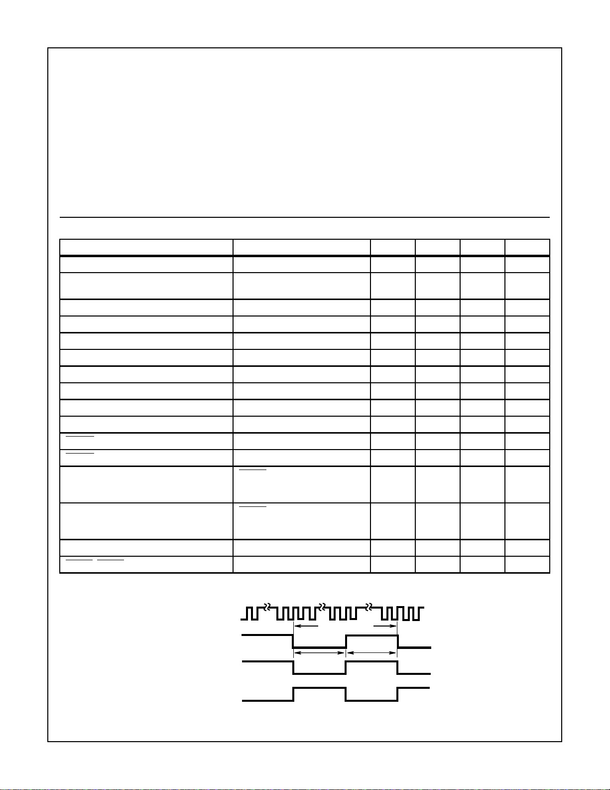
Timing Waveforms
OSCILLATOR
FREQUENCY
BACKPLANE
INPUT/OUTPUT
OFF SEGMENTS
ON SEGMENTS
FIGURE 1. ICM7224 DISPLAY WAVEFORMS
128 CYCLES
64 CYCLES
64 CYCLES
9-16
Page 4

Typical Performance Curves
ICM7224
30
LCD DEVICES, TEST CIRCUIT
DISPLAY BLANK
25
PIN 36 OPEN
20
15
10
SUPPLY CURRENT (µA)
5
0
1234567
TA = 25oC
SUPPLY VOLTAGE (V)
TA = -20oC
TA = 70oC
FIGURE 2. OPERA TING SUPPLY CURRENT AS A FUNCTION
OF SUPPLY VOLTAGE
45
SINE WAVE INPUT
SWINGING FULL SUPPLY
40
35
TA = -20oC
1000
LCD DEVICES
T
= 25oC
A
V
= 5V
SUPPLY
100
HZ
OSC
128
ƒ
BP =
ƒ
10
V
= 4V
SUPPLY
V
SUPPLY
1
1 10 100 1000
= 3V
C
OSC
V
SUPPLY
(pF)
= 6V
FIGURE 3. BACKPLANE FREQUENCY AS A FUNCTION OF
OSCILLATOR CAPACITOR C
10
V+ = 5V
TA = 25oC
1
OSC
30
ƒMAX (MHz)
25
20
15
456
SUPPLY VOLTAGE (V)
FIGURE 4. MAXIMUM COUNT FREQUENCY (TYPICAL) AS A
FUNCTION OF SUPPLY VOLTAGE
TA = 25oC
TA = 70oC
0.1
SUPPLY CURRENT (mA)
0.01
1kHz 10kHz 100kHz 1MHz 10MHz 100MHz
ƒCOUNT
FIGURE 5. SUPPLY CURRENT AS A FUNCTION OF COUNT
FREQUENCY
TABLE 1. CONTROL INPUT DEFINITIONS
TERMINAL INPUT VOLTAGE FUNCTION
29 Leading Zero Blanking VDD or Floating Leading Zero Blanking Enabled
INput V
SS
Leading Zeroes Displayed
31 COUNT INHIBIT VDD or Floating Counter Enabled
V
SS
Counter Disabled
33 RESET VDD or Floating Inactive
V
SS
Counter Reset to 0000
34 STORE VDD or Floating Output Latches not Updated
V
SS
Output Latches Updated
9-17
Page 5

ICM7224
Control Input Definitions
In Table 1, VDD and VSS are considered to be normal operating input logic levels. Actual input low and high levels are
specified in the Operating Characteristics. For lowest power
consumption, input signals should swing over the full supply.
Detailed Description
The ICM7224 provides outputs suitable for driving conven-
1
tional 4
29 individual segment drivers, a backplane driver, and a selfcontained oscillator and divider chain to generate the backplane frequency (See Functional Block Diagram).
The segment and backplane drivers each consist of a
CMOS inverter, with the N-Channel and P-Channel devices
ratioed to provide identical on resistances, and thus equal
rise and fall times. This eliminates any DC component which
could arise from differing rise and fall times, and ensures
maximum display life.
The backplane output can be disabled by connecting the
OSCILLATOR input (pin 36) to V
29 segment outputs directly with a signal input at the BP terminal (pin 5) and allows cascading of several slave devices
to the backplane output of one master device. The backplane may also be derived from an external source. This
allows the use of displays with characters in multiples of four
and a single backplane. A slave device will represent a load
of approximately 200pF (comparable to one additional segment). The limitation on the number of devices that can be
slaved to one master device backplane driver is the additional load represented by the larger backplane of displays of
more than four digits, and the effect of that load on the backplane rise and fall times. A good rule of thumb to observe in
order to minimize power consumption, is to keep the rise and
fall times less than about 5 microseconds. The backplane
driver of one device should handle the back-plane to a display of 16 one-half-inch characters without the rise and fall
times exceeding 5µs (i.e., 3 slave devices and the display
backplane driven by a fourth master device). It is recommended that if more than four devices are to be slaved
together, that the backplane signal be derived externally and
all the lCM7224 devices be slaved to it.
This external backplane signal should be capable of driving
very large capacitive loads with short (1-2µs) rise and fall
times. The maximum frequency for a backplane signal
should be about 150Hz, although this may be too fast for
optimum display response at lower display temperatures,
depending on the display used.
The onboard oscillator is designed to free run at approximately
19kHz, at microampere power levels. The oscillator frequency
is divided by 126 to provide the backplane frequency, which
will be approximately 150Hz with the oscillator free-running.
The oscillator frequency may be reduced by connecting an
external capacitor between the OSCillator terminal (pin 36)
and V
“Typical Performance Curves” for detailed information.
The oscillator may also be overdriven if desired, although
care must be taken to insure that the backplane driver is not
/2 digit by seven segment LCD displays. It includes
. This synchronizes the
SS
; see the plot of oscillator/back-plane frequency in
DD
disabled during the negative portion of the overdriving signal
(which could cause a DC component to the display). This
can be done by driving the OSCILLATOR input between the
positive supply and a level out of the range where the backplane disable is sensed, about one fifth of the supply voltage
above the negative supply. Another technique for overdriving
the oscillator (with a signal swinging the full supply) is to
skew the duty cycle of the overdriving signal such that the
negative portion has a duration shorter than about one
microsecond. The backplane disable sensing circuit will not
respond to signals of this duration.
Counter Section
The lCM7224 implements a four-digit ripple carry resettable
counter, including a Schmitt trigger on the COUNT input and
a
CARRY output. Also included is an extra D-type flip-flop,
clocked by the
segment driver. This output driver can be used as either a
true half-digit or as an overflow indicator. The counter will
increment on the negative-going edge of the signal at the
COUNT input, while the
going edge following the count which increments the counter
from 9999 to 10000. Once the half-digit flip-flop has been
clocked, it can only be reset (with the rest of the counter) by
a negative level at the
four decades will continue to count in a normal fashion after
the half-digit is set, and subsequent
be affected.
A negative level at the
first divide-by-two in the counter chain without affecting its
clock. This provides a true inhibit, not sensitive to the state of
the COUNT input, which prevents false counts that can
result from using a normal logic gate to prevent counting.
Each decade of the counter directly drives a four-to-seven
segment decoder which develops the required output data.
The output data is latched at the driver. When the
pin is low, these latches are updated, and when it is high or
floating, the latches hold their contents.
The decoders also include zero detect and blanking logic to
provide leading zero blanking. When the Leading Zero
Blanking INput is floating or at a positive lev el, this circuitry is
enabled and the device will blank leading zeroes. When it is
low, or the half-digit is set, leading zero blanking is inhibited,
and zeroes in the four digits will be displayed. The Leading
Zero Blanking OUTput is provided to allow cascaded
devices to blank leading zeroes correctly. This output will
assume a positive level only when all four digits are blanked;
this can only occur when the Leading Zero Blanking INput is
at a positive level and the half-digit is not set.
For example, in an eight-decade counter with overflow using
two lCM7224 devices, the Leading Zero Blanking OUTput of
the high order digit would be connected to the Leading Zero
Blanking INput of the low order digit device. This will assure
correct leading zero blanking for all eight digits.
The
STORE, RESET, COUNT INHIBIT, and Leading Zero
Blanking INputs are provided with pullup devices, so that
they may be left open when a positive level is desired. The
CARRY and Leading Zero Blanking OUTputs are suitable for
CARRY signal which controls the half-digit
CARRY output provides a negative-
RESET terminal, pin 33. However, the
CARRY outputs will not
COUNT INHIBIT input disables the
STORE
9-18
Page 6

ICM7224
interfacing to CMOS logic in general, and are specifically
designed to allow cascading of the devices in four-digit
blocks.
Applications
Figure 8 shows an 8-digit precision frequency counter. The
circuit uses two ICM7224s cascaded to provide an 8-digit
display. Backplane output of the second device is disabled
and is driven by the first device. The
second device is used for overflow indication. The input signal is fed to the first device and the COUNT input of the second is driven by the
CARRY output of the first. Notice that
leading zero blanking is controlled on the second device and
the LZB OUT of the second one is tied to LZB IN of the first
one. An ICM7207A device is used as a timebase generator
and frequency counter controller. It generates count window,
store and reset signals which are directly compatible with
ICM7224 inputs (notice the need for an inverter at
INHIBIT input). The ICM7207A provides two count window
signals (1s and 0.1s gating) for displaying frequencies in Hz
or tens of Hz (x10Hz).
5V
-
+
1
/2 digit output of the
COUNT
a
f
b
g
e
c
d
DP
200pF
200pF
200pF
200pF
EACH SEGMENT TO
BACKPLANE WITH
200pF CAPACITOR
1
V
DD
2
ICM7224
3
4
5
BP
OSCILLATOR
6
7
8
9
10
11
12
13
14
15
16
17
18
19
20
COUNT
COUNT INHIBIT
LZB OUT
CARRY
1
/2 DIGIT
V
SS
STORE
RESET
LZB IN
40
39
38
37
36
35
34
33
32
31
30
29
28
27
26
25
24
23
22
21
FIGURE 7. SEGMENT ASSIGNMENT AND DISPLAY FONT
(BLANK)
FIGURE 6. TEST CIRCUIT
9-19
Page 7

ICM7224
20
HIGH ORDER DIGITS
SLAVE BACKPLANE
21
SWITCH CLOSED INHIBITS
LEADING ZERO BLANKING
10kΩ
3V - 6V
-
+
V
DD
C
OUT
1 OVERFLOW
ICM7224
27
1
2
3
4
5
6
7
ICM7207A
C
IN
6 SEG
CARRY
LZB IN
28
29
HIGH ORDER DIGITS
15 SEG
COUNT INHIBIT
LZB OUT
COUNT
RESET
33
32
31
30
14
13
12
11
10
9
8
5
BP
STORE
OSC
V
SS
36
35
34
SWITCH OPEN
s GATING
1
SWITCH CLOSED
s GATING
0.1
CRYSTAL
= 22pF
C
IN
= 22pF
C
OUT
= 5.24288MHz
f
O
< 75Ω
R
S
= 0.015pF
C
S
= 3.5pF
C
P
3 SEG
4 SEG
1
V
DD
40
LOW ORDER DIGITS
1 BACKPLANE
6 SEG
20
LOW ORDER DIGITS
MASTER BACKPLANE
21
15 SEG
ICM7224
1
/4 CD4069C
LZB OUT
CARRY
LZB IN
28
30
29
27
CONDITIONING
(PRESCALER
LEVEL SHIFTING)
8-DIGIT LCD DISPLAY
WITH OVERFLOW
COUNT INHIBIT
COUNT
STORE
RESET
V
SS
35
34
33
32
31
INPUT
SIGNAL
4 SEG
5
BP
OSC
36
3 SEG
1
V
DD
40
INPUT SIGNAL
FIGURE 8. EIGHT-DIGIT PRECISION FREQUENCY COUNTER
All Intersil semiconductor products are manufactured, assembled and tested under ISO9000 quality systems certification.
Intersil products are sold by description only. Intersil Corporation reserves the right to make changes in circuit design and/or specifications at any time without
notice. Accordingly, the reader is cautioned to verify that data sheets are current before placing orders. Information furnished by Intersil is believed to be accurate
and reliable. However, no responsibility is assumed b y Intersil or its subsidiaries for its use; nor for any infringements of patents or other rights of third parties which
may result from its use. No license is granted by implication or otherwise under an y patent or patent rights of Intersil or its subsidiaries.
For information regarding Intersil Corporation and its products, see web site http://www.intersil.com
9-20
 Loading...