

Page 1
August 1997
ICM7211, ICM7212
4-Digit, ICM7211 (LCD) and
ICM7212 (LED) Display Drivers
Features ICM7211 (LCD)
• Four Digit Non-Multiplexed 7 Segment LCD Display
Outputs with Backplane Driver
• Complete Onboard RC Oscillator to Generate Backplane
Frequency
• Backplane Input/Output Allows Simple Synchronization
of Slave-Devices to a Master
• ICM7211 Devices Provide Separate Digit Select Inputs to
Accept Multiplexed BCD Input (Pinout and Functionally
Compatible with Siliconix DF411)
• ICM7211M Devices Provide Data and Digit Address
Latches Controlled by Chip Select Inputs to Provide a
Direct High Speed Processor Interface
• ICM7211 Decodes Binary to Hexadecimal; ICM7211A
Decodes Binary to Code B (0-9, Dash, E, H, L, P, Blank)
• ICM7211A Available in Surface Mount Package
Features ICM7212AM (LED)
• 28 Current-Limited Segment Outputs Provide 4-Digit
Non-Multiplexed Direct LED Drive at >5mA Per Segment
• Brightness Input Allows Direct Control of LED
Segment Current with a Single Potentiometer or
Digitally as a Display Enable
• ICM7212AM Device Provides Same Input Configuration
and Output Decoding Options as the ICM7211AM
Description
The ICM7211 (LCD) and ICM7212 (LED) devices constitute
a family of non-multiplexed four-digit seven-segment CMOS
display decoder-drivers.
The ICM7211 devices are configured to drive conventional
LCD displays by providing a complete RC oscillator, divider
chain, backplane driver, and 28 segment outputs.
The ICM7212 devices are configured to drive commonanode LED displays, providing 28 current-controlled, low
leakage, open-drain N-Channel outputs. These devices
provide a brightness input, which may be used at normal
logic levels as a display enable, or with a potentiometer as a
continuous display brightness control.
These devices are available with multiplexed or microprocessor input configurations. The multiplexed versions provide f our
data inputs and four Digit Select inputs. This configuration is
suitable for interfacing with multiplexed BCD or binary output
devices, such as the ICM7217, ICM7226, and ICL7135. The
microprocessor versions provide data input latches and Digit
Address latches under control of high-speed Chip Select
inputs. These devices simplify the task of implementing a
cost-effective alphanumeric seven-segment display for microprocessor systems, without requiring extensive ROM or CPU
time for decoding and display updating.
The standard devices will provide two different decoder
configurations. The basic device will decode the four bit
binary inputs into a seven-segment alphanumeric hexadecimal output. The “A” versions will provide the “Code B” output
code, i.e., 0-9, dash, E, H, L, P, blank. Either device will correctly decode true BCD to seven-segment decimal outputs.
Ordering Information
DISPLAY
PART NUMBER
ICM7211lPL LCD Hexadecimal Multiplexed Direct Drive -40 to 85 40 Ld PDIP E40.6
ICM7211MlPL LCD Hexadecimal Microprocessor Direct Drive -40 to 85 40 Ld PDIP E40.6
ICM7211AlPL LCD Code B Multiplexed Direct Drive -40 to 85 40 Ld PDIP E40.6
ICM7211AMlPL LCD Code B Microprocessor Direct Drive -40 to 85 40 Ld PDIP E40.6
ICM7211AlM44 LCD Code B Multiplexed Direct Drive -40 to 85 44 Ld MQFP Q44.10x10
ICM7211AMlM44 LCD Code B Microprocessor Direct Drive -40 to 85 44 Ld MQFP Q44.10x10
ICM7212AMlPL LED Code B Microprocessor Common Anode -40 to 85 40 Ld PDIP E40.6
CAUTION: These devices are sensitive to electrostatic discharge; follow proper IC Handling Procedures.
http://www.intersil.com or 407-727-9207
TYPE
DISPLAY
DECODING
| Copyright © Intersil Corporation 1999
INPUT
INTERFACING
DISPLAY DRIVE
9-6
TYPE
TEMP .
RANGE (oC) PACKAGE PKG. NO.
File Number 3158.1
Page 2
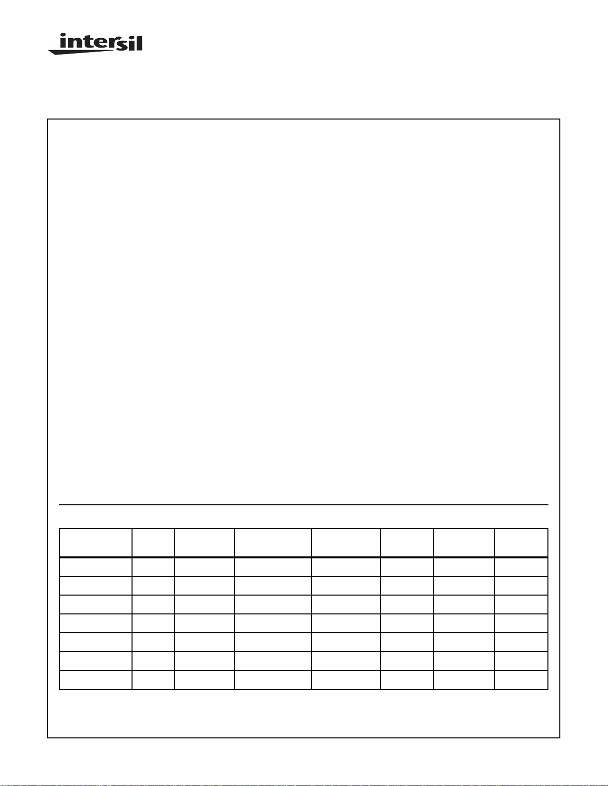
Pinouts
V
DD
e1
g1
BP
a2
b2
c2
d2
e2
g2
a3
b3
c3
d3
e3
g3
a4
ICM7211, ICM7212
ICM7211, ICM7211A
(PDIP)
TOP VIEW
1
2
3
4
f1
5
6
7
8
9
10
11
12
f2
13
14
15
16
17
18
19
f3
20
d1
40
c1
39
b1
38
a1
37
OSC
36
V
35
SS
D4
34
DIGIT
D3
33
32
31
30
29
28
27
26
25
24
23
22
21
D2
D1
B3
B2
B1
B0
f4
g4
e4
d4
c4
b4
SELECT
INPUTS
DAT A
INPUTS
V
DD
e1
g1
f1
BP
a2
b2
c2
d2
e2
g2
f2
a3
b3
c3
d3
e3
g3
f3
a4
ICM7211M, ICM7211AM
(PDIP)
TOP VIEW
1
2
3
4
5
6
7
8
9
10
11
12
13
14
15
16
17
18
19
20
40
d1
39
c1
38
b1
37
a1
36
OSC
35
V
SS
CHIP SELECT 2
34
CHIP SELECT 1
33
DIGIT ADRESS BIT 2
32
DIGIT ADRESS BIT 1
31
B3
30
B2
29
28
27
26
25
24
23
22
21
B1
B0
f4
g4
e4
d4
c4
b4
DAT A
INPUTS
V
DD
e1
g1
BRT
a2
b2
c2
d2
e2
g2
a3
b3
c3
d3
e3
g3
a4
ICM7212AM
(PDIP)
TOP VIEW
1
2
3
4
f1
5
6
7
8
9
10
11
12
f2
13
14
15
16
17
18
19
f3
20
40
d1
39
c1
38
b1
37
a1
36
V
SS
V
35
SS
34
CHIP SELECT 2
33
CHIP SELECT 1
32
DIGIT ADRESS BIT 2
31
DIGIT ADRESS BIT 1
30
B3
29
B2
DAT A
B1
B0
f4
g4
e4
d4
c4
b4
INPUTS
28
27
26
25
24
23
22
21
9-7
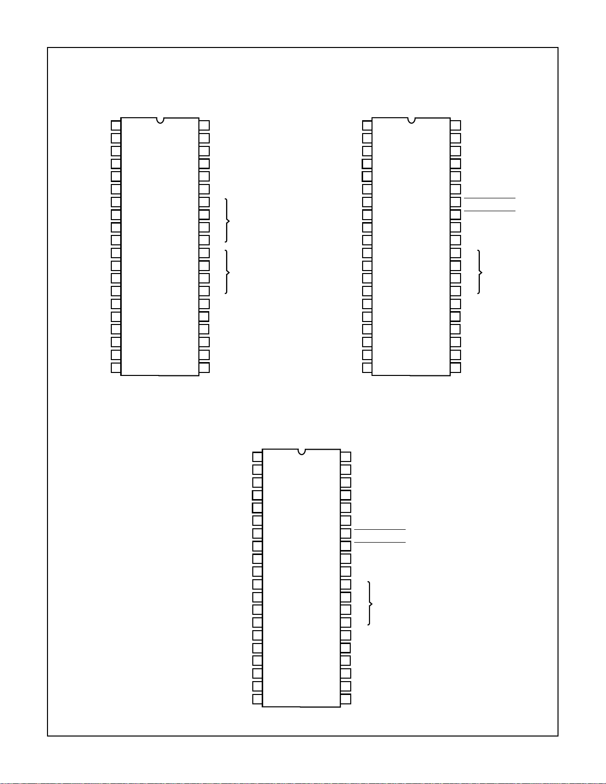
Page 3
ICM7211, ICM7212
Pinouts
(Continued)
a2
b2
c2
d2
e2
NC
g2
d3
b3
c3
ICM7211A
(MQFP)
TOP VIEW
BP
f1
44 43 42 41 40
1
2
3
4
5
6
7
f2
8
9
10
11
12 13 14 15 16 17
e3
d3
DD
NC
V
d1
e1
g1
f3
a4
g3
c1
39 38 37 36 35 34
c4d4e4
b4
NC
OSC
b1
a1
33
32
31
30
29
28
27
26
25
24
23
2221201918
V
D4
D3
D2
D1
NC
B3
B2
B1
B0
f4
SS
DIGIT
SELECT
INPUTS
DAT A
INPUTS
g4
a2
b2
c2
d2
e2
NC
g2
d3
b3
c3
ICM7211AM
(MQFP)
TOP VIEW
DD
NC
V
d1
BP
f1
e1
g1
44 43 42 41 40
1
2
3
4
5
6
7
f2
8
9
10
11
12 13 14 15 16 17
f3
e3
d3
g3
a4
c1
39 38 37 36 35 34
c4d4e4
b4
NC
OSC
b1
a1
V
33
32
31
30
29
28
27
26
25
24
23
2221201918
SS
CHIP SELECT 2
CHIP SELECT 1
DIGITAL ADRESS BIT 2
DIGITAL ADRESS BIT 1
NC
B3
B2
DAT A
INPUTS
B1
B0
f4
g4
9-8
Page 4
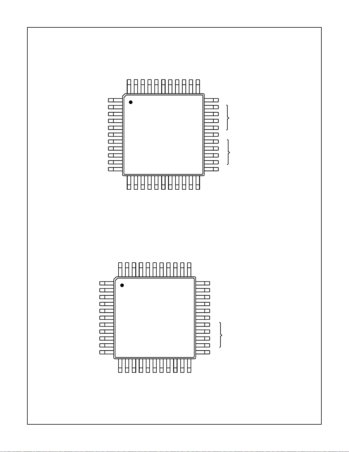
ICM7211, ICM7212
Functional Block Diagrams
D4
SEGMENT OUTPUTS
7 WIDE DRIVER
7 WIDE LATCH EN
PROGRAMMABLE
4 TO 7 DECODER
DAT A
INPUTS
DIGIT
SELECT
INPUTS
OSCILLATOR
INPUT
ENABLE
DIRECTOR
ICM7211A
D3
SEGMENT OUTPUTS
7 WIDE DRIVER
7 WIDE LATCH EN
PROGRAMMABLE
4 TO 7 DECODER
OSCILLATOR
19kHz
FREE-RUNNING
SEGMENT OUTPUTS
7 WIDE DRIVER
7 WIDE LATCH EN
PROGRAMMABLE
4 TO 7 DECODER
÷128
D2
BLACKPLANE
DRIVER
ENABLE
SEGMENT OUTPUTS
D1
7 WIDE DRIVER
7 WIDE LATCH EN
PROGRAMMABLE
4 TO 7 DECODER
BP INPUT/OUTPUT
DAT A
INPUTS
2-BIT
DIGIT
ADRESS
INPUT
CHIP
SELECT 1
CHIP
SELECT 2
OSCILLATOR
INPUT
4-BIT
LATCH
ENABLE
2-BIT
LATCH
ENABLE
SEGMENT OUTPUTS
D4
7 WIDE DRIVER
7 WIDE LATCH EN
PROGRAMMABLE
4 TO 7 DECODER
2 TO 4
DECODER
ONE
SHOT
ENABLE
DIRECTOR
ICM7211AM
D3
SEGMENT OUTPUTS
7 WIDE DRIVER
7 WIDE LATCH EN
PROGRAMMABLE
4 TO 7 DECODER
OSCILLATOR
19kHz
FREE-RUNNING
SEGMENT OUTPUTS
7 WIDE DRIVER
7 WIDE LATCH EN
PROGRAMMABLE
4 TO 7 DECODER
÷128
D2
BLACKPLANE
DRIVER
ENABLE
SEGMENT OUTPUTS
D1
7 WIDE DRIVER
7 WIDE LATCH EN
PROGRAMMABLE
4 TO 7 DECODER
BP INPUT/OUTPUT
9-9
Page 5

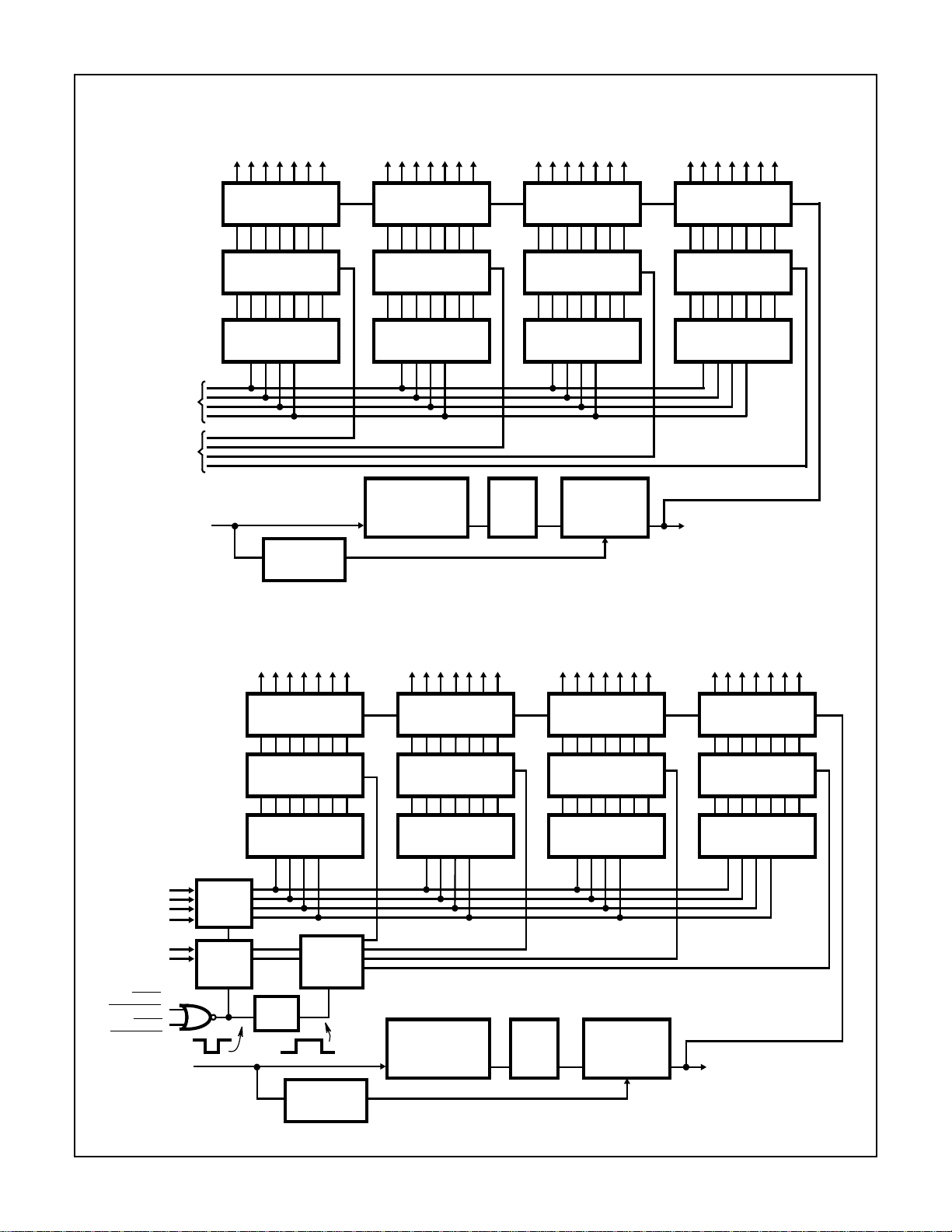
ICM7211, ICM7212
Functional Block Diagrams
D4
7 WIDE DRIVER
7 WIDE LATCH EN
PROGRAMMABLE
4 TO 7 DECODER
2 TO 4
DECODER
ONE
SHOT
DAT A
INPUTS
2-BIT
DIGIT
ADRESS
INPUT
CHIP
SELECT 1
CHIP
SELECT 2
SEGMENT OUTPUTS
4-BIT
LATCH
ENABLE
2-BIT
LATCH
ENABLE
(Continued)
SEGMENT OUTPUTS
ICM7212AM
D3
7 WIDE DRIVER
7 WIDE LATCH EN
PROGRAMMABLE
4 TO 7 DECODER
SEGMENT OUTPUTS
D2
7 WIDE DRIVER
7 WIDE LATCH EN
PROGRAMMABLE
4 TO 7 DECODER
SEGMENT OUTPUTS
D1
7 WIDE DRIVER
BRIGHTNESS
7 WIDE LATCH EN
PROGRAMMABLE
4 TO 7 DECODER
9-10
Page 6

ICM7211, ICM7212
Absolute Maximum Ratings Thermal Information
Supply Voltage (VDD - VSS). . . . . . . . . . . . . . . . . . . . . . . . . . . .6.5V
Input Voltage (Any Terminal) (Note 1) . . VSS- 0.3V to VDD, + 0.3V
Operating Conditions
Temperature Range . . . . . . . . . . . . . . . . . . . . . . . . . . -40oC to 85oC
CAUTION: Stresses above those listed in “Absolute Maximum Ratings” may cause permanent damage to the device. This is a stress only rating and operation
of the device at these or any other conditions above those indicated in the operational sections of this specification is not implied.
NOTES:
1. Due to the SCR structure inherent in the CMOS process, connecting any terminal to voltages greater than VDD or less than VSS may
cause destructive device latchup. For this reason, it is recommended that no inputs from external sources not operating on the same
power supply be applied to the device before its supply is established, and that in multiple supply systems, the supply to the ICM7211
and ICM7212 be turned on first.
2. θJA is measured with the component mounted on an evaluation PC board in free air.
Electrical Specifications
PARAMETER TEST CONDITIONS MIN TYP MAX UNITS
ICM7211 CHARACTERISTICS (LCD) VDD = 5V ±10%, TA = 25oC, VSS = 0V Unless Otherwise Specified
Operating Supply Voltage Range (VDD - VSS), V
Operating Current, I
Oscillator Input Current, I
Segment Rise/Fall Time, tr, t
Backplane Rise/Fall Time, tr, t
Oscillator Frequency, f
Backplane Frequency, f
DD
OSCI
f
f
OSC
BP
ICM7212 CHARACTERISTICS (Common Anode LED)
Operating Supply Voltage Range (VDD - VSS), V
Operating Current Display Off, I
Operating Current, I
DD
Segment Leakage Current, I
Segment On Current, I
SEG
STBY
SLK
INPUT CHARACTERISTICS (ICM7211 and ICM7212)
Logical “1” Input Voltage, V
Logical “0” Input Voltage, V
Input Leakage Current, I
Input Capacitance, C
BP/Brightness Input Leakage, I
BP/Brightness Input Capacitance, C
IH
IL
ILK
lN
BPLK
BPI
AC CHARACTERISTICS - MULTIPLEXED INPUT CONFIGURATION
Digit Select Active Pulse Width, t
Data Setup Time, t
Data Hold Time, t
DS
DH
Inter-Digit Select Time, t
WH
IDS
AC CHARACTERISTICS - MICROPROCESSOR INTERFACE
Chip Select Active Pulse Width, t
Data Setup Time, t
Data Hold Time, t
DS
DH
Inter-Chip Select Time, t
WL
ICS
SUPPLY
Test circuit, Display blank - 10 50 µA
Pin 36 - ±2 ±10 µA
CL = 200pF - 0.5 - µs
CL = 5000pF - 1.5 - µs
Pin 36 Floating - 19 - kHz
Pin 36 Floating - 150 - Hz
SUPPLY
Pin 5 (Brightness), Pins 27-34 V
Pin 5 at VDD, Display all 8’s - 200 - mA
Segment Off - ±0.01 ±1 µA
Segment On, VO = +3V 5 8 - mA
Pins 27-34 - ±0.01 ±1 µA
Pins 27-34 - 5 pF
Measured at Pin 5 with Pin 36 at V
All Devices - 200 - pF
Refer to Timing Diagrams 1 - - µs
Other Chip Select Either Held Active,
or Both Driven Together
Thermal Resistance (Typical, Note 2) θJA (oC/W)
PDIP Package. . . . . . . . . . . . . . . . . . . . . . . . . . . . . 60
MQFP Package. . . . . . . . . . . . . . . . . . . . . . . . . . . . 80
Maximum Junction Temperature. . . . . . . . . . . . . . . . . . . . . . . 150oC
Maximum Storage Temperature Range . . . . . . . . . .-65oC to 150oC
Maximum Lead Temperature (Soldering, 10s) . . . . . . . . . . . . 300oC
(MQFP - Lead Tips Only)
356V
456V
SS
-1050µA
4--V
--1V
SS
- ±0.01 ±1 µA
500 - - ns
200 - - ns
2--µs
200 - - ns
100 - - ns
10 0 - ns
2--µs
9-11
Page 7

ICM7211, ICM7212
Input Definitions In this table, V
and VSS are considered to be normal operating input logic levels. Actual input low and high le vels are
DD
specified under Operating Characteristics. For lowest po wer consumption, input signals should s wing o v er the full supply.
INPUT TERMINAL CONDITIONS FUNCTION
B0 27 V
= Logical One
DD
Ones (Least Significant)
VSS = Logical Zero
B1 28 V
= Logical One
DD
Twos
VSS = Logical Zero
B2 29 V
= Logical One
DD
Fours
VSS = Logical Zero
B3 30 V
= Logical One
DD
Eights (Most Significant)
VSS = Logical Zero
OSC (LCD Devices
Only)
36 Floating or with External
Capacitor to V
V
SS
DD
Oscillator Input
Disables BP output devices, allowing segments to be synchronized to
an external signal input at the BP terminal (Pin 5).
ICM7211 Multiplexed-Binary Input Configuration
INPUT TERMINAL CONDITIONS FUNCTION
D1 31 V
D2 32 D2 Digit Select
= Inactive
DD
VSS = Active
D1 Digit Select (Least Significant)
D3 33 D3 Digit Select
D4 34 D4 Digit Select (Most Significant)
ICM7211M/ICM7212M Microprocessor Interface Input Configuration
INPUT DESCRIPTION TERMINAL CONDITIONS FUNCTION
DA1 Digit Address
Bit 1 (LSB)
DA2 Digit Address
Bit 2 (MSB)
CS1 Chip Select 1 33 VDD = Inactive
CS2 Chip Select 2 34 VDD = Inactive
31 VDD = Logical One
VSS = Logical Zero
32 VDD = Logical One
VSS = Logical Zero
VSS = Active
VSS = Active
DA1 and DA2 serve as a 2-bit Digit Address Input
DA2, DA1 = 00 selects D4
DA2, DA1 = 01 selects D3
DA2, DA1 = 10 selects D2
DA2, DA1 = 11 selects D1
When both CS1 and CS2 are taken low, the data at the Data
and Digit Select code inputs are written into the input latches.
On the rising edge of either Chip Select, the data is decoded
and written into the output latches.
Data Input Bits
Timing Diagrams
DIGIT SELECT
DIGIT SELECT
CS1
(CS2)
CS2
(CS1)
DATA AND
DIGIT
ADDRESS
D
N-1
D
N
DATA VALID
D
N-1
t
IDS
t
WH
DATA VALID
D
N
t
DS
FIGURE 1. MULTIPLEXED INPUT
t
WI
t
DS
= DON’T CARE
t
ICS
t
DH
FIGURE 2. MICROPROCESSOR INTERFACE INPUT
t
IDS
t
DH
9-12
Page 8

Typical Performance Curves
ICM7211, ICM7212
30
LCD DEVICES, TEST CIRCUIT
DISPLAY BLANK, PIN 36 OPEN
25
4123 675
SUPP
TA = -20oC
TA = 70oC
(V)
20
TA = 25oC
15
(µA)
OP
I
10
5
V
FIGURE 3. ICM7211 OPERA TING SUPPLY CURRENT AS A
FUNCTION OF SUPPLY VOLTAGE
15
PIN 5 AT VDD, TA = 25oC
V
= 6V
SUPP
10
V
= 5V
(mA)
SEG
I
5
V
SUPP
SUPP
= 4V
180
LCD DEVICES, TA = 25oC
(Hz)
BP
ƒ
150
120
90
60
30
0
C
= 0pF
OSC
(PIN 36 OPEN)
V
C
OSC
4123 65
(V)
SUPP
C
OSC
= 22pF
= 220pF
FIGURE 4. ICM7211 BA CKPLANE FREQUENCY AS A
FUNCTION OF SUPPLY VOLTAGE
12
SEGMENT OUTPUT AT +3V
= 25oC
T
A
10
8
(mA)
6
SEG
I
4
0
4123 65
VO(V)
FIGURE 5. ICM7212 LED SEGMENT CURRENT AS A
FUNCTION OF OUTPUT VOLTAGE
1800
LED DEVICES, DISPLAY ALL EIGHTS
LED FORWARD VOLTAGE DROP
1500
1200
900
POWER (mW)
600
300
0
= 1.7V, PIN 5 AT VDD, TA = 25oC
V
FLED
FIGURE 7. ICM7212 OPERATING POWER (LED DISPLAY) AS A FUNCTION OF SUPPLY VOLTAGE
465
V
SUPP
2
0
0
VOLTAGE ON BRT PIN 5 (V)
4123 65
FIGURE 6. ICM7212 LED SEGMENT CURRENT AS A
FUNCTION OF BRIGHTNESS CONTROL VOLTAGE
(V)
9-13
Page 9

ICM7211, ICM7212
Description Of Operation
LCD Devices
The LCD devices in the family (ICM7211, ICM7211A,
ICM7211M, ICM7211AM) provide outputs suitable for driving
conventional four-digit, seven-segment LCD displays. These
devices include 28 individual segment drivers, backplane
driver, and a self-contained oscillator and divider chain to
generate the backplane frequency.
The segment and backplane drivers each consist of a
CMOS inverter, with the N-Channel and P-Channel devices
ratioed to provide identical on resistances, and thus equal
rise and fall times. This eliminates any DC component, which
could arise from differing rise and fall times, and ensures
maximum display life.
The backplane output devices can be disabled by connecting the OSCillator input (pin 36) to V
segment outputs to be synchronized directly to a signal input
at the BP terminal (pin 5). In this manner, several slave
devices may be cascaded to the backplane output of one
master device, or the backplane may be derived from an
external source. This allows the use of displays with characters in multiples of four and a single backplane. A slave
device represents a load of approximately 200pF (comparable to one additional segment). Thus the limitation of the
number of devices that can be slaved to one master device
backplane driver is the additional load represented by the
larger backplane of displays of more than four digits. A good
rule of thumb to observe in order to minimize power consumption is to keep the backplane rise and fall times less
than about 5µs. The backplane output driver should handle
the backplane to a display of 16 one-half inch characters. It
is recommended, if more than four devices are to be slaved
together, the backplane signal be derived externally and all
the ICM7211 devices be slaved to it. This external signal
should be capable of driving very large capacitive loads with
short (1 - 2µs) rise and fall times. The maximum frequency
for a backplane signal should be about 150Hz although this
may be too fast for optimum display response at lower display temperatures, depending on the display type.
The onboard oscillator is designed to free run at approximately 19kHz at microampere current levels. The oscillator
frequency is divided by 128 to provide the backplane frequency , which will be appro ximately 150Hz with the oscillator
free-running; the oscillator frequency may be reduced by
connecting an external capacitor between the OSCillator terminal and V
DD
.
The oscillator may also be overdriven if desired, although care
must be taken to ensure that the backplane driver is not disabled during the negative portion of the overdriving signal
(which could cause a DC component to the display). This can
be done by driving the OSCillator input between the positive
supply and a level out of the range where the bac kplane disable
is sensed (about one fifth of the supply voltage above V
Another technique for overdriving the oscillator (with a signal
swinging the full supply) is to skew the duty cycle of the overdriving signal such that the negative portion has a duration
shorter than about one microsecond. The backplane disable
sensing circuit will not respond to signals of this duration.
. This allows the 28
SS
SS
OSCILLATOR
FREQUENCY
BACKPLANE
INPUT/OUTPUT
OFF
SEGMENTS
ON
SEGMENTS
FIGURE 8. DISPLAY WAVEFORMS
128 CYCLES
64 CYCLES
64 CYCLES
LED Devices
The LED device in the family (ICM7212AM) pro vides outputs
suitable for directly driving four-digit, seven-segment
common-anode LED displays. These devices include 28
individual segment drivers, each consisting of a low-leakage,
current-controlled, open-drain, N-Channel transistor.
The drain current of these transistors can be controlled by
varying the voltage at the BRtrighTness input (pin 5). The voltage at this pin is transferred to the gates of the output devices
for “on” segments, and thus directly modulates the transistor’s
“on” resistance. A brightness control can be easily implemented with a single potentiometer controlling the voltage at
pin 5, connected as in Figure 9. The potentiometer should be
a high value (100kΩ to 1MΩ) to minimize pow er consumption,
which can be significant when the display is off.
V
(LED ANODES)
DD
100kΩ TO 1MΩ
FIGURE 9. BRIGHTNESS CONTROL
The brightness input may also be operated digitally as a display enable; when high, the display is fully on, and low fully
off. The display brightness ma y also be controlled by varying
the duty cycle of a signal swinging between the two voltages
at the brightness input.
Note that the LED device has two connections for V
of these pins should be connected. The double connection is
necessary to minimize effects of bond wire resistance with
the large total display currents possible.
When operating LED devices at higher temperatures and/or
higher supply voltages, the device power dissipation may
need to be reduced to prevent excessive chip temperatures.
The maximum power dissipation is 1W at 25
early above 35
o
35
).
C). Power dissipation for the device is given by:
P = (V
SUPP
where V
segment current, and n
o
C to 500mW at 70oC (-15mW/oC above
- V
FLED
)(l
FLED
SEG
is the LED forward voltage drop, I
SEG
It is recommended that if the device is to be operated at
BRIGHTNESS
PIN 5
o
C, derated lin-
)(n
)
SEG
is the number of “on” segments.
SS
; both
SEG
is
9-14
Page 10

ICM7211, ICM7212
elevated temperatures the segment current be limited b y use
of the brightness input to keep power dissipation within the
limits described above.
Input Configurations and Output Codes
The standard devices in the ICM7211 and ICM7212 family
accept a four-bit true binary (i.e., positive level = logical one)
input at pins 27 thru 30, least significant bit at pin 27 ascending to the most significant bit at pin 30. The ICM7211 and
ICM7211M devices decode this binary input into a sevensegment alphanumeric hexadecimal output, while the
ICM7211A, ICM7211AM, and ICM7212AM decode the
binary input into seven-segment alphanumeric “Code B” output, i.e., 0-9, dash, E, H, L, P, blank. These codes are shown
explicitly in Table 1. Either decoder option will correctly
decode true BCD to a seven-segment decimal output.
TABLE 1. OUTPUT CODES
BlNARY
HEXADECIMAL
ICM7211
ICM7211M
0000
0001
0010
CODE B
ICM7211A
ICM7212AMB3 B2 B1 BO
These devices are actually mask-programmable to provide
any 16 combinations of the seven segment outputs decoded
from the four input bits. For large quantity orders custom
decoder options can be arranged. Contact the factory for
details.
The ICM7211 and ICM7211A devices are designed to accept
multiplexed binary or BCD input. These devices provide four
separate digit lines (least significant digit at pin 31 ascending
to most significant digit at pin 34), each of which when taken
to a positive level decodes and stores in the output latches of
its respective digit the character corresponding to the data at
the input port, pins 27 through 30.
The ICM7211M, ICM7211AM, and ICM7212AM devices are
intended to accept data from a data bus under processor
control.
In these devices, the four data input bits and the two-bit digit
address (DA1 pin 31, D A2 pin 32) are written into input buff er
latches when both chip select inputs (
CS1 pin 33, CS2 pin
34) are taken low. On the rising edge of either chip select
input, the content of the data input latches is decoded and
stored in the output latches of the digit selected by the contents of the digit address latches.
An address of 00 writes into D4, DA2 = 0, DA1 = 1 writes into
D3, DA2 = 1, DA1 = 0 writes into D2, and 11 writes into D1.
The timing relationships for inputting data are shown in
Figure 2, and the chip select pulse widths and data setup and
hold times are specified under Operating Characteristics.
0011
0100
0101
0110
0111
1000
1001
1010
1011
1100
1101
1110
1111 BLANK
a
f
b
g
e
c
d
FIGURE 10. SEGMENT ASSIGNMENT
9-15
Page 11

Test Circuit
ICM7211, ICM7212
V
DD
+ -
V
SS
EACH SEGMENT
OUTPUT TO
BACKPLANE
WITH A 200pF
CAP A CIT OR
10
11
12
13
14
15
16
17
18
19
20
1
2
3
4
5
6
7
8
9
V
BP
DD
ICM7211AM
DIGIT/CHIP
SELECT
INPUTS
DAT A
INPUTS
FIGURE 11.
OSC
V
SS
40
39
38
37
36
35
34
33
32
31
30
29
28
27
26
25
24
23
22
21
MICROPROCESSOR
V
DD
VERSION
MULTIPLEXED
V
SS
VERSION
V
DD
Typical Applications
LCD DISPLAY
+5V
BCD/BINARY
DAT A
D8
D7
D6
DIGIT
SELECTS
D5
D4
D3
D2
D1
8-DIGIT
D8 D7 D6 D5 D4 D3 D2 D1
BACKPLANE
SLAVE
V
DD
V
SS
OSC
B3-B0 D4 D3 D2 D1 BP
4
28
SEGMENTS
HIGH ORDER
ICM7211A
4
+5V
BACKPLANE
MASTER
V
DD
V
SS
OSC
B3-B0 D4 D3 D2 D1 BP
BACKPLANE
28
SEGMENTS
LOW ORDER
ICM7211A
4
FIGURE 12. GANGED ICM7211’s DRIVING 8-DIGIT LCD DISPLAY
9-16
Page 12

ICM7211, ICM7212
Typical Applications
+5V
26
INPUT
NC
40
V
CCVDD
2 XTAL1
3 XTAL2
4
RESET
7 EA
5 SS
1 TO
39 T1
6
INT
PSENALE
11 9 25
20
V
SS
80C48
µCOMPUTER
PROG
WR
(Continued)
P10 27
28
29
30
31
32
33
P17 34
P20 21
22
23
24
35
36
37
P27 38
DB0 12
13
14
15
16
17
18
DB7
19
RD
10 8
ICM7211M
HIGH ORDER DIGITS
1 V
+5V
I/O
I/O
DD
35 V
SS
36 OSC
SEGMENTS
27 28 29 30
DAT A
B0-B3
2, 3, 4
6-26
37-40
DS1 DS2
31 32 33 34
BP 5
CS1
8 DIGIT
LCD DISPLAY
CS2
BP 5
DAT A
B0-B3
2, 3, 4
6-26
37-40
DS1 DS2 CS1
292827 30
ICM7211M
LOW ORDER DIGITS
SEGMENTS
CS2
31 32 33 34
1 V
35 V
36 OSC
DD
SS
+5V
FIGURE 13. 80C48 MICROPROCESSOR INTERFACE
All Intersil semiconductor products are manufactured, assembled and tested under ISO9000 quality systems certification.
Intersil products are sold by description only. Intersil Corporation reserves the right to make changes in circuit design and/or specifications at any time without
notice. Accordingly, the reader is cautioned to verify that data sheets are current before placing orders. Information furnished by Intersil is believed to be accurate
and reliable. However, no responsibility is assumed by Intersil or its subsidiaries f or its use; nor for any infringements of patents or other rights of third parties which
may result from its use. No license is granted by implication or otherwise under an y patent or patent rights of Intersil or its subsidiaries.
For information regarding Intersil Corporation and its products, see web site http://www.intersil.com
9-17
 Loading...