

Page 1
October 1999
TM
ICL8211, ICL8212
T
C
U
D
O
O
C
E
R
O
N
M
M
N
E
R
D
E
D
E
L
O
S
B
C
A
L
P
E
O
R
P
E
T
T
N
E
M
E
Prog rammable Voltage Detect ors
Features
• High Accuracy Voltage Sensing and Generation
• Internal Reference 1.15V Typical
• Low Sensitivity to Supply Voltage and Temperature
Variations
• Wide Supply Voltage Range Typ. 1.8V to 30V
• Essentially Constant Supply Current Over Full Supply
Voltage Range
• Easy to Set Hysteresis Volt age Range
• Defined Output Current Limit ICL8211
• High Output Current Capability ICL8212
Applications
• Low Voltage Sensor/Indicator
• Hi g h Volta ge Sens or/Indi c ator
• Nonvolatile Out-of-Voltage Range Sensor/Indicator
• Programmable Voltage Reference or Zener Diode
• Series or Shunt Power Supply Regulator
• Fixed Value Constant Current Source
Description
The Intersil ICL8211/8212 are micropower bipolar monolithic
integrated circuits intended primarily for precise voltage
detection and generation. These circuits consist of an
accurate voltage reference, a comparator and a pair of
output buff er/drivers.
Specifically, the ICL8211 provides a 7mA current limited output sink when the voltage applied to the ‘THRESHOLD’
terminal is less than 1.15V (the internal reference). The
ICL8212 requires a voltage in excess of 1.15V to switch its
output on (no current limit). Both devices have a low current
output (HYSTERESIS) which is switched on for input
voltages in excess of 1.15V. The HYSTERESIS output may
be used to provide positive and noise free output switching
using a simple feedback network.
Ordering Information
PART NUMBER
ICL8211CPA 0
ICL8211CBA 0
ICL8211CTY 0
ICL8211MTY
(Note 1)
ICL8212CPA 0
ICL8212CBA 0
ICL8212CTY 0
ICL8212MTY
(Note 1)
NOTE:
1. Add /883B to part number if 883B processing is required
TEMPERATURE
RANGE PACKAGE
o
C to +70oC 8 Lead Plastic DIP
o
C to +70oC 8 Lead SOlC (N)
o
C to +70oC 8 Pin Metal Can
o
C to +125oC 8 Pin Metal Can
-55
o
C to +70oC 8 Lead Plastic DIP
o
C to +70oC 8 Lead SOlC (N)
o
C to +70oC 8 Pin Metal Can
o
C to +125oC 8 Pin Metal Can
-55
Pinouts
ICL8 211 (PDIP, SOIC)
TOP VIEW
NC
1
HYSTERESIS
THRESHOLD
OUTPUT
CAUTION: These devices are sensitive to electrostatic discharge; follow proper IC Handling Procedures.
1-888-INTERSIL or 321-724-7143
Copyright © Intersil Americas Inc. 2002. All Rights Reserved
2
3
4
| Intersil (and design) is a trademark of Intersil Americas Inc.
8
V+
7
NC
6
NC
5
GROUND
7-161
THRESHOLD
OUTPUT
NC
ICL8211 (CAN)
TO P VIEW
HYSTERESIS
8
1
2
3
4
GROUND
7
V+
6
NC
5
NC
FN3184.2
Page 2
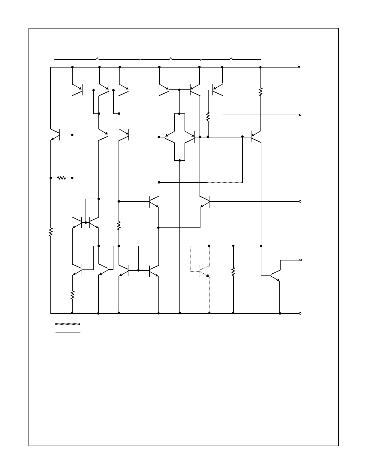
Functional Diagram
VOLTAGE REFERENCE COMPARATOR OUTPUT BUFFERS
ICL8211, ICL8212
8
V+
R1
20MΩ
Q1
Q7
Q2
Q3
Q5
1.15V
Q23
Q4
Q6
V
REF
R3
360kΩ
Q16
Q12
Q14 Q15
Q17 Q18
R4
1MΩ
Q13
X X X X
Q19
R5
4.5kΩ
2
HYST
3
THRESHOLD
Q8
R2
30kΩ
X X X X X X
Q9
ICL8211 OPTION
ICL8212 OPTION
Q10
Q11
Q20
R6
100kΩ
Q21
4
5
OUTPUT
GROUND
7-162
Page 3
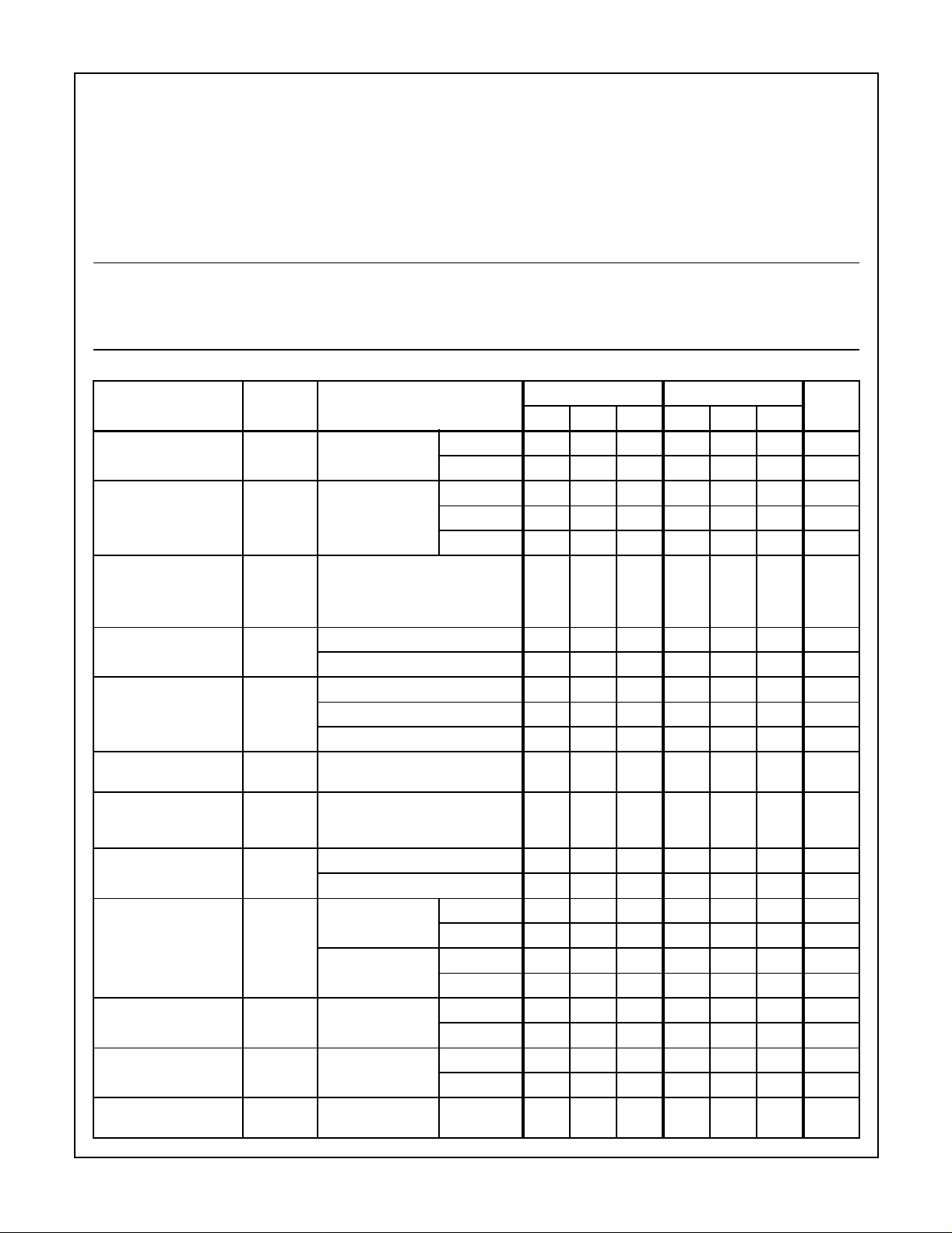
Specifications ICL8211, ICL8212
Absolute Maximum Ratings Thermal Information
Supply Voltage . . . . . . . . . . . . . . . . . . . . . . . . . . . . . . -0.5V to +30V
Output Voltage . . . . . . . . . . . . . . . . . . . . . . . . . . . . . . -0.5V to +30V
Hysteresis Voltage . . . . . . . . . . . . . . . . . . . . . . . . . . . +0.5V to -10V
Threshold Input Voltage . . . . . . . . . . . . . +30V to -5V with respect to
GROUND and +0V to -30V with respect to V+
Current into Any Terminal . . . . . . . . . . . . . . . . . . . . . . . . . . . . . . ± 30mA
CAUTION: Stresses above those listed i n “Abso lute Ma ximum Rati ngs ” may cause pe rmanent dam age to the dev ice. T his is a str ess only rating and operation
of the device at these or any other conditions above those indicated in the operational sections of this specification is not implied.
Operating C o ndi t io ns
Operating Temperature Range
ICL8211M/8212M . . . . . . . . . . . . . . . . . . . . . . . . -55
ICL8211C/8212C . . . . . . . . . . . . . . . . . . . . . . . . . . .0
o
C to +125oC
o
C to +70oC
Thermal Resistance θ
Plastic DIP Package . . . . . . . . . . . . . . . . 150oC/W -
Plastic SOIC Package . . . . . . . . . . . . . . . 180
Metal Can . . . . . . . . . . . . . . . . . . . . . . . . 156
JA
o
C/W -
o
C/W 68oC/W
Lead Temperature (Soldering, 10s). . . . . . . . . . . . . . . . . . . . . 300
θ
JC
o
(SOIC - Lead Tips Only)
Current into Any Terminal . . . . . . . . . . . . . . . . . . . . . . . . . . . . . . ± 30mA
o
Storage Temperature Range . . . . . . . . . . . . . . . . . . -65
C to +150oC
C
Electrical Specifications V+ = 5V, T
= +25oC Unless Otherwise Specified
A
PARAMETER SYMBOL TEST CONDITIONS
Supply Current I+ 2.0 < V+ < 30 V
Threshold Trip Vo ltage V
Threshold Voltage
Dispari ty Between
Outp ut & Hy s tere s is
Output
Guara n tee d O pe r ati ng
V
Supply Voltage Range
Minimum Operating
V
Supply Voltage Range
V
THP
SUPPLY
SUPPLY
I
TH
OUT
V
OUT
I
OUT
I
HYST
V
OUT
V
HYST
= 4mA
= 2V
= 4mA
= 7mA
= 2V
= 3V
+25oC (Note 3) 2.0 - 30 2.0 - 30 V
0oC to +70oC (Note 3) 2.2 - 30 2.2 - 30 V
+25oC-1.8--1.8-V
o
+125
C-1.4--1.4-V
-55oC-1.5--2.5-V
Threshold Voltage Tem-
∆V
TH
/∆TI
OUT
= 4mA, V
= 2V - ± 20 0 - - ± 200 - ppm/oC
OUT
perature C oeffi ci en t
Variation of Threshold
Voltag e w ith Su pp ly
∆V
/∆V+ ∆V+ = 10% at V+ = 5V - 1.0 - - 1.0 - mV
TH
Voltage
Threshold Input Current I
Outp ut Le ak ag e Current I
Output Satura ti on
Voltage
Max Available Output
Current
Hystere sis Leakage
Current
TH
OLK
V
SAT
I
OH
I
LHYS
VTH = 1.15V - 100 250 - 100 250 nA
V
= 1.00V - 5 - - 5 - nA
TH
V
= 30V VTH = 0.9V-----10µA
OUT
V
= 5V VTH = 0.9V-----1µA
OUT
I
= 4mA VTH = 0.9V - 0.17 0.4 - - - V
OUT
(Notes 3 & 4)
V
= 5V
OUT
V+ = 10V,
V
= GND
HYST
ICL8211 ICL8212
UNITSMIN TYP MAX MIN TYP MAX
= 1.3V 10 22 40 50 110 250 µA
TH
VTH = 0.9V 50 140 250 10 20 40 µA
V+ = 5V 0.98 1.15 1.19 1.00 1.15 1.19 V
V+ = 2V 0.98 1.145 1.19 1.00 1.145 1.19 V
V+ = 30V 1.00 1.165 1.20 1.05 1.165 1.20 V
--0.8- --0.5- mV
VTH = 1.3V--10---µA
V
= 1.3V--1---µA
TH
V
= 1.3V----0.170.4V
TH
= 0.9V 4 7.0 12 - - - mA
V
TH
VTH = 1.3V - - - 15 35 - mA
= 1.0V - - 0.1 - - 0.1 µA
V
TH
7-163
Page 4
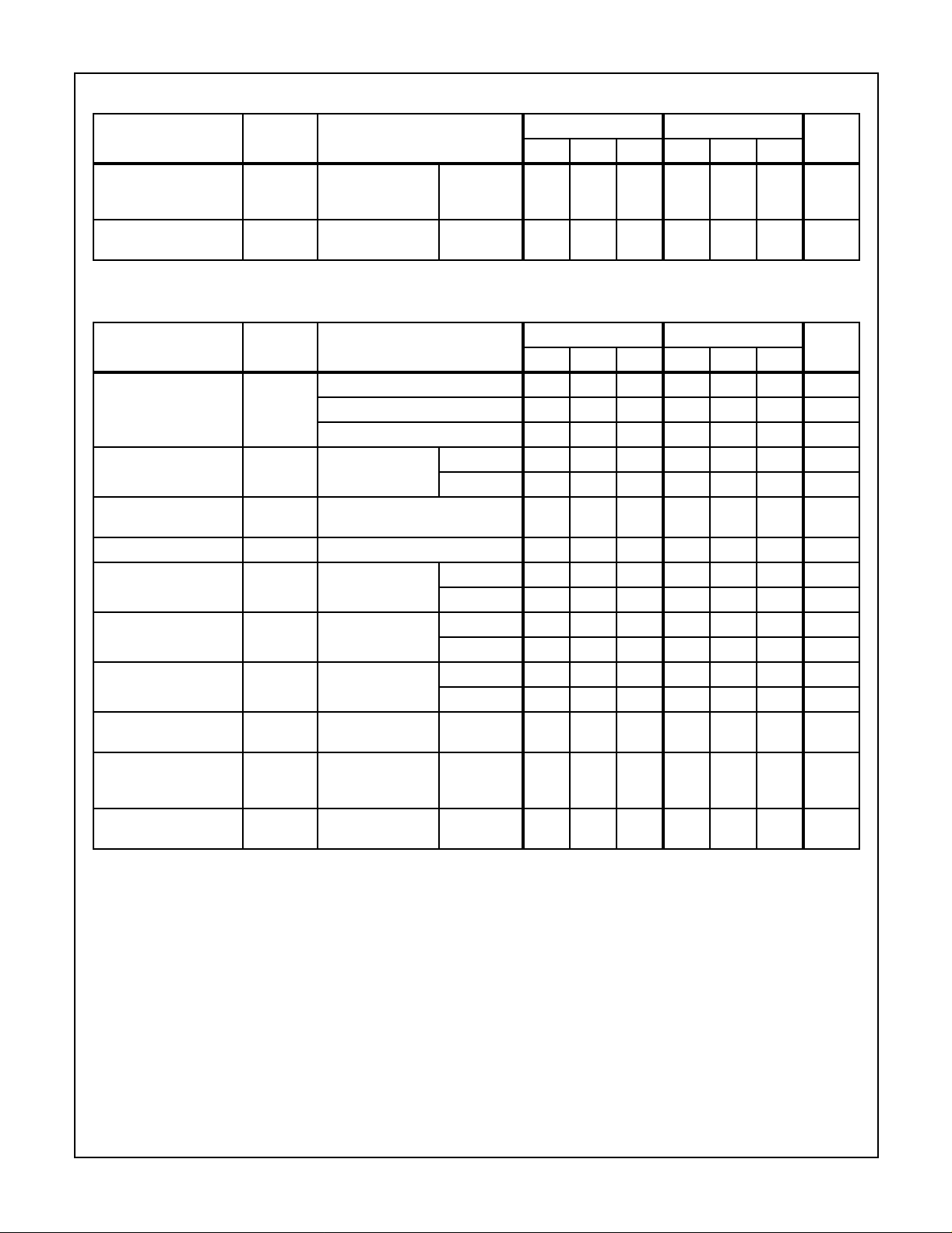
ICL8211, ICL8212
Electrical Specifications V+ = 5V, T
= +25oC Unless Otherwise Specified (Continued)
A
ICL8211 ICL8212
PARAMETER SYMBOL TEST CONDITIONS
Hysteresis Sat Voltage V
HYS(MAX)IHYST
= -7µA,
measured with
V
= 1.3V - -0.1 -0.2 - -0.1 -0.2 V
TH
UNITSMIN TYP MAX MIN TYP MAX
respect to V+
Max Available
Hysteresis Curre nt
I
HYS (M A X)
Electrical Specifications ICL8211MTY/8212MTY V+ = 5V, T
VTH = 1.3V -15 -21 - -15 -21 - µA
= -55oC to +125oC
A
ICL8211 ICL8212
PARAMETER SYMBOL TEST CONDITIONS
UNITSMIN TYP MAX MIN TYP MAX
Supply Current I+2.8 < V+ < 30 ------ -
V
= 1.3V - - 100 - 350 350 µA
T
VT = 0.8V - - 350 - 100 100 µA
Threshold Trip Vo ltage V
Guara n tee d O pe r ati ng
V
Supply Voltage Range
Threshold Input Current I
Outp ut Le ak ag e Current I
Output Satura ti on
Voltage
Max Available Output
Current
Hystere sis Leakage
Current
Hysteresis Saturation
Voltage
V
HYS(MAX)IHYST
SUPPLY
TH
OLK
V
SAT
I
OH
I
LHYS
I
TH
OUT
V
OUT
= 2mA
= 2V
V+ = 2.8V 0.80 - 1.30 0.80 - 1.30 V
V+ = 30V 0.80 - 1.30 0.80 - 1.30 V
(Note 5) 2.8 - 30 2.8 - 30 V
VTH = 1.15V - - 400 - - 400 nA
V
= 30V VTH = 0.8V-----20µA
OUT
V
= 1.3V--20---µA
TH
I
= 3mA VTH = 0.8V--0.5---V
OUT
VTH = 1.3V-----0.5V
(Notes 3 & 4)
V
= 5V
OUT
V+ = 10V
V
= GND
HYST
= -7µA
= 0.8 3 - 15 - - - mA
V
TH
V
= 1.3V---9--mA
TH
= 0.8V - - 0.2 - - 0.2 µA
V
TH
VTH = 1.3V - - 0.3 - - 0.3 V
measured with
respect to V+
Max Available
Hysteresis Curre nt
I
HYS (M A X)
VTH = 1.3V 10 - - 10 - - µA
NOTES:
1. The maximum output current of the ICL8211 is limited by design to 15mA under any operating conditions. The output voltage may be
sustained at any voltage up to +30V as long as the maximum power dissipation of the device is not exceeded.
2. The ma ximum outp ut curre nt of the ICL 8212 is not de fined. And sy stems usi ng th e ICL8 212 mu st ther efor e ensure that th e out put current
does not exceed 30mA and that the maximum power dissipation of the device is not exceeded.
3. Threshold Trip Voltage is 0.80V(min) to 1.30V(mas). At I
OUT
= 3mA.
7-164
Page 5
ICL8211, ICL8212
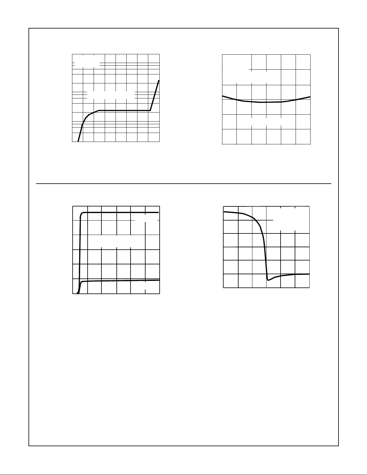
Typical Performance Curves (ICL8211 and ICL8212)
10,000
THRESHOLD INPUT CURRENT (nA)
TA = +25oC
V+ = +10V
1,000
ICL8211 OR ICL8212
100
10
0.0 1.1 1.15 1.2 2.0 3.0 6.0 8.0 10.0
THRESHOLD VOLTAGE (V
(IRREGULAR SCALE)
)
TH
FIGURE 1. THRESHOLD INPUT CURRENT AS A FUNCTION OF
THRESHOLD VOLTAGE
Typical Performance Curves
150
125
100
75
TA = +25oC
OUTPUTS OPEN CIRCUIT
(ICL8211 ONLY)
VTH = 0.9V
0
V+ = +5V
= 1.2V
V
TH
V
-5
= 4.5V
HYS
(OR -0.5V WITH RESPECT
TO V+ SUPPLY)
-10
-20
-25
ICL8211 OR ICL8212
-30
HYSTERESIS OUTPUT CURRENT (µA)
-40 -20 0 +20 +40 +60 +80
TEMPERATURE (
o
C)
FIGURE 2. HYSTERESIS OUTPUT SATURATION CURRENT AS
A FUNCTION OF TEMPERATURE
150
125
100
75
TA = +25oC
V+ = +5V
OUTPUTS OPEN
CIRCUIT
50
SUPPLY CURRENT (µA)
25
VTH = 1.3V
0102030
SUPPLY VOLTAGE
FIGURE 3. SUPPLY CURRENT AS A FUNCTION OF SUPPLY
VOLTAGE
50
SUPPLY CURRENT (µA)
25
0
0.0 1.0 1.1 1.15 1.2 2.0 4.0
THRESHOLD VOLTAGE (V
(IRREGULAR SCALE)
)
TH
FIGURE 4. SUPPLY CURRENT AS A FUNCTION OF THRESH-
OLD VOLTAGE
7-165
Page 6

ICL8211, ICL8212
Typical Performance Curves (ICL8211 ONLY) (Continued)
150
125
100
75
50
SUPPLY CURRENT (µA)
25
0
-55 -25 +5 +35 +65 +95 +125
VTH = 0.9V
VTH = 1.3V
TEMPERATURE
o
C
FIGURE 5. SUPPLY CURRENT AS A FUNCTION OF TEMPERA-
TURE
OUTPUT
1.15
1.14
HYSTERESIS OUTPUT
12
10
8
6
OUTPUT
4
OUTPUT CURRENT (mA)
2
0
1.12 1.13 1.14 1.15 1.16 1.17 1.18
THRESHOLD VOLTAGE
TA = +25oC
V+ = +5V
V
= 0.5V
O
V
= V+ - 0.25V
HYS
HYSTERESIS
OUTPUT
8mV
0
-5
-10
-15
-20
-25
-30
HYSTERESIS OUTPUT CURRENT (µA)
FIGURE 6. OUTPUT SATURATION CURRENTS AS A FUNC-
TION OF THRESHOLD VOLTAGE
1.18
IO = 4mA, VO = 1V
I
1.17
1.16
1.15
= -7µA, V
HYS
HYS
OUTPUT
= (V+ -2) V
THRESHOLD VOLTAGE
1.13
-55 -25 +5 +35 +65 +95 +125
V+ = +5V
= 1mA, V
I
O
= -7µA, V
I
HYS
TEMPERATURE (
= +5V
OUT
= 0V
HST
o
C)
FIGURE 7. THRESHOLD VOLTAGE TO TURN OUTPUTS “JUST
ON” AS A FUNCTION OF TEMPERATURE
8
7
6
OUTPUT CURRENT (mA)
5
-55 -25 +5 +35 +65 +95 +125
TEMPERATURE (
V+ = +5V
V
= 1.1V
TH
= 1.0V
V
O
o
C)
THRESHOLD VOLTAGE
1.14
1.13
1 2 3 4 5 10 20 304050 100
HYSTERESIS OUTPUT
SUPPLY VOLTAGE
FIGURE 8. THRESHOLD VOLTAGE TO TURN OUTPUTS “JUST
ON” AS A FUNCTION OF SUPPLY VOLTAGE
12
TA = +25oC
V+ = +5V
9
VTH = 1.0V
6
3
OUTPUT CURRENT (mA)
0
0.1 1.0 10.0 100.0
VTH = 1.147V
VTH = 1.152V
OUTPUT VOLTAGE
FIGURE 9. OUTPUT SATURATION CURRENT AS A FUNCTION
OF TEMPERATURE
0
µA)
FIGURE 10. OUTPUT CURRENT AS A FUNCTION OF OUTPUT
VOLTAGE
7-166
Page 7

ICL8211, ICL8212
Typical Performance Curves (ICL8212 ON LY)
150
TA = +25oC
OUTPUTS OPEN CIRCUIT
125
100
75
50
SUPPLY CURRENT (µA)
25
0
0102030
VTH = 1.3V
VTH = 0.9V
SUPPLY VOLTA G E
FIGURE 12. SUPPLY CURRENT AS A FUNCTION OF SUPPLY
VOLTAGE
150
V+ = 5V
OUTPUTS
125
OPEN
CIRCUIT
100
75
50
SUPPLY CURRENT - I+ (µA)
25
0
-55 -25 +5 +35 +65
TEMPERATURE (oC)
VTH = 1.3V
VTH = 0.9V
+95
+125
150
TA = +25oC
V+ = +5V
125
OUTPUTS OPEN CIRCUIT
100
75
50
SUPPLY CURRENT - I+ (µA)
25
0
0.0 1.0 1.1 1.15 1.2 2.0 4.0
THRESHOLD VOLTAGE (V
(IRREGULAR SCALE)
)
TH
FIGURE 13. SUPPLY CURRENT AS A FUNCTION OF THRESH-
OLD VOLTAGE
30
25
TA = +25oC
20
15
10
OUTPUT CURRENT (mA)
5
0
1.14 1.15 1.16 1.17 1.18 1.19 1.20
OUTPUT
THRESHOLD VOLTAGE
V+ = 5V
= 4V
V
OUT
= V+ -0.25V
V
HYS
HYSTERESIS OUTPUT
0
-5
-10
-15
-20
-25
HYSTERESIS OUTPUT CURRENT (µA)
-30
FIGURE 14. SUPPLY CURRENT AS A FUNCTION OF TEMPER-
ATURE
1.17
IO = 1mA, V
I
= -7µA, V
HYS
1.16
1.15
THRESHOLD VOLTAGE
1.14
-55 -25 +5 +35 +65 +95 +125
= 5V
OUT
= 0V
HYS
BOTH OUTPUT AND
HYSTERESIS OUTPUT
TEMPERATURE (
o
C)
FIGURE 16. THRESHOLD VOLTAGE TO TURN OUTPUTS “JUST
ON” AS A FUNCTION OF TEMPERATURE
FIGURE 15. OUTPUT SATURATION CURRENTS AS A FUNC-
TION OF THRESHOLD VOLTAGE
1.18
1.17
1.16
BOTH OUTPUT AND
1.15
THRESHOLD VOLTAGE
1.14
1.13
123451020304050100
HYSTERESIS OUTPUT
TA = +25oC
= 4mA, V
I
OUT
I
= -7µA, V
HYS
SUPPLY VOLTAGE
OUT
HYS
= 1V
= (V+ -2) V
FIGURE 17. THRESHOLD VOLTAGE TO TURN OUTPUTS “JUST
ON” AS A FUNCTION OF SUPPLY VOLTAGE
7-167
Page 8

ICL8211, ICL8212
Typical Performance Curves
(ICL8212 ONLY) (Continued)
0.6
0.5
0.4
0.3
0.2
0.1
OUTPUT SATURATION VOLTAGE
0
-55 - 25 +5 +35 +65 +95 +1 25
FIGURE 18. OUTPUT SATURATION VOLTAGE AND CURRENT
AS A FUNCTION OF TEMPERATURE
40
TA = +25oC
V+ = +5V
30
OUTPUT SAT.
CURRENT
(VO = 4.0V)
VOLTAGE SAT.
CURRENT
(I
TEMPERATURE (
VTH =1.25V
= 10mA)
O
V+ = +5V
V
TH
o
C)
= 1.2V
Detailed Description
The ICL8211 and ICL8212 use standard linear bipolar
integrated circuit technology with high value thin film
resistors which define extremely low value currents.
Components Q
accurate voltage reference of 1.15V. This reference voltage
is close to the value of the bandgap voltage for silicon and is
highly stable with respect to both temperature and supply
voltage. The deviation from the bandgap voltage is
necessary due to the negative temperature coefficient of the
thin film resis tors (-5000 ppm per
Components Q
current source; Q
mirror. Q
8
current mirror, the collector currents of Q
to be equal and it can be shown that the collector current in
Q
and Q9 is
8
or approximately 1µA at +25
Where k = Boltzman’s Constant
q = Charge on an Electron
and T = Absolute Temperature in
through Q10 and R1, R2 and R3 set up an
1
o
C).
through Q9 and R2 make up a constant
2
and Q3 are identical and form a current
2
has 7 times the emitter area of Q9, and due to the
and Q9 are forced
8
IC (Q8 or Q9) =
1
R2 q
o
C
kT
x
o
K
In7
20
VTH = 1.158V
10
OUTPUT CURRENT (mA)
VTH = 1.153V
0
0.1 1.0 10.0 30.0 100.0
OUTPUT VOLTAGE
FIGURE 19. OUTPUT CURRENT AS A FUNCTION OF OUTPUT
VOLTAGE
0
-5
-10
-15
-20
-25
-30
-35
HYSTERESIS OUTPUT CURRENT (µA)
-40
-10.00 -1.00 -0.10 -0.01
VT = 1.152V
VT = 1.153V
VT = 1.18V
TA = +25oC
V+ = +10V
HYSTERESIS OUTPUT VOLTAGE
FIGURE 20. HYSTERESIS OUTPUT CURRENT AS A FUNCTION
OF HYSTERESIS OUTPUT VOLTAGE
Transistors Q
and Q
9
, Q6, and Q7 assure that the VCE of Q3, Q4,
5
remain constant with supply voltage variations. This
ensures a constant current supply free from variations.
The base current of Q
provides sufficient start up current for
1
the constant source; there being two stable states for this
type of circuit - either ON as defin ed above, or OFF if no star t
up current is provided. Leakage current in the transistors is
not suffi cient in itself to guarantee reliable startup.
Q
is matched to Q3 and Q2; Q10 is matche d to Q9. Thus the
4
IC and V
of Q10 are identical to that of Q9 or Q8. To
BE
generate the bandgap voltage, it is necessary to sum a
voltage equal to the base emitter voltage of Q
to a voltage
9
proportional to the difference of the base emitter voltages of
two transistors Q
Thus 1. 5 = V
which provides :
and Q9 operating at two current densities.
8
BE (Q9
or Q10) +
R
3
= 12 (approximately.)
R
2
R
3
R
2
kT
x
q
The total su pply current consu med by the voltage re ference
section is approximately 6µA at room temperature. A voltage
at the THRESHOLD input is compared to the reference 1.15V
by the compa rator consisti ng of transisto rs Q
through Q17.
11
The outputs from the comparator are limited to two diode
drops less t ha n V + or approxim a t ely 1 . 1V. Thus the base current into the hysteresis output transistor is limited to about
500nA and the collector current of Q
In the case of the ICL8211, Q
times the emitter area of Q
20
to 100µA.
19
is proportioned to have 70
21
thereby limiting the output
current to approximately 7mA, whereas for the ICL8212
7-168
Page 9

ICL8211, ICL8212
I
(
R
)
S
almost all the collector current of Q19 is available for base
drive to Q
, resulting in a maximum available collector
21
current of the order of 30mA. I t i s advisable to ext ernally limit
this current to 25mA or l ess.
Applications
The ICL8211 and ICL8212 are similar in many respects, especially with regard to the setup of the input trip conditions and
hysteresis circuitry. The following discussion describes both
devices, and where differences occur they are clearly not ed.
General Inf orma t ion
Threshold Input Considerations
Although any voltage betwee n -5V and V+ may be applied to
the THRESHOLD terminal, it is recommended that the
THRESHOLD voltage does not exceed about +6V since
above that voltage the threshold input current increases
sharply. Also, prolonged operation above this voltage will
lead to degradat ion of device characteristics.
The outputs change states with an input THRESHOLD
voltage of approximately 1.15V. Input and output waveforms
are shown in Figure 21 for a si mp le 1. 15V level detector.
R
L1
V+
(V+ MUST BE
EQUAL OR
EXCEED 1.8V
V
HYST
V
O
NPUT VOLTAGE
RECOMMENDED
ANGE -5 TO +5V)
V
TH
1
2
3
4
8
7
6
5
such as TTL or CMOS using a single pullup resist or. There is
a guaranteed TTL fanout of 2 for the ICL8211 and 4 for the
ICL8212.
A principal application of the ICL8211 is voltage level
detection, and for that re ason the OUTPUT curre nt has been
limited to typically 7mA to permit direct drive of an LED
connected to the positive supply without a series current
limiting re s is to r.
On the other hand the ICL8212 is intended for applications
such as programmable zener references, and voltage
regulators where output currents well in excess of 7mA are
desirable. Therefore, the output of the ICL8212 is not current
limited, and if the output is used to drive an LED, a series
current limiting resistor must be used.
In most applications an input resistor divider network may be
used to generate the 1.15V required for V
. For high accu-
TH
racy, currents as large as 50µA may be used, however for
those applications where current limiting may be desirable,
(such as when operating from a battery) currents as low as
6mA may be considered without a great loss of accuracy.
6mA represents a practical minimum, since it is about this
level where the device’s own input current becomes a significant percent age of that flowing in the divider network.
V+
1
2
V
TH
3
4
8
7
6
5
PULLUP RESISTOR
CMOS OR
TTL GATE
R
L2
V
O2
1.15V
0
V+
0V
V+
0V
ICL8211 OUTPUT
ICL8212 OUTPUT
FIGURE 21. VOLTAGE LEVEL DETECTION
The HYSTERESIS output is a low current output and is
intended primarily for input threshold voltage hysteresis
applications. If this output is used for other applications it is
suggested that output currents be limited to 10µA or less.
The regular OUTPUT’s from either the ICL8211 or ICL8212
may be used to drive most of the common logic families
V
O1
FIGURE 22. OUTPUT LOGIC INTERFACE
INPUT
R
2
V
R
1
V-
1
2
TH
3
4
V+
8
7
6
5
FIGURE 23. INPUT RESISTOR NETWORK CONSIDERATIONS
Case 1. High accu racy required, current in resistor n etwork
unimportant Set I = 5 0µA for V
= 1.15V ∴ R1 →
TH
20kΩ
Case 2. Good accuracy required, current in resistor network
important Set I = 7.5µA for V
= 1.15V ∴ R1 →
TH
150kΩ
7-169
Page 10

ICL8211, ICL8212
V+
INPUT
INPUT
VOLT AGE
V-
R
2
R
1
1
2
3
4
8
7
6
5
Input voltage to change to output states
(R
+ R2)
1
=
x 1.15V
R
1
FIGURE 24. RANGE OF INPUT VOLTAGE GREATER THAN
+1.15 VOLTS
Setup Procedures For Voltage Level Detection
Case 1. Simple voltage detection no hysteresis
Unless an input voltage of approximately 1.15V is to be
detected, resistor networks will be used to divide or multiply
the unknown voltage to be sensed. Figure 25 shows
procedures on how to set up resistor networks to detect
INPUT VOL TAGES of any magnitude and polarity.
MAY BE ANY STABLE VOLTAGE
VOLTAGE REFERENCE
GREATER THAN 1.15V
1
2
3
4
8
7
6
5
V+
R
V
2
REF (+VE)
R
1
Case 2. Use of the HYSTERESIS function
The disadvantage of the simple detection circuits is that
there is a small but finite input range where the outputs are
neither totally ‘ON’ nor totally ‘OFF’. The principle behind
hysteresis is to provide positive feedback to the input trip
point such that there is a voltage difference between the
input voltage necessary to turn the outputs ON and OFF.
The advantage of hysteresis is especially apparent in
electrically noisy environments where simple but positive
voltage detection is required. Hysteresis circuitry, however,
is not limited to applications requiring better noise performance but may be expanded into highly complex systems
with multiple voltage level detection and memory applications-refer to specific applications section.
There are two simple methods to apply hysteres is to a circuit
for use in supply voltage level detecti o n. These are shown in
Figure 27.
The circuit of Fi gure 27A requires that the full current flowing
in the resistor network be sourced by the HYSTERESIS output, whereas for circuit Figure 27B the current to be sourced
by the HYSTERESIS output will be a function of the ratio of
the two trip points and their val ues. For low values of hysteresis, circuit Figure 27B is to be preferred due to the offset
voltage of t he hysteresis output transistor.
A third way to obtain hysteresis (ICL8211 only) is to connect
a resistor between the OUTPUT and the THRESHOLD
terminals thereby reducing the total external resistance
between the THRESHOLD and GROUND when the
OUTPUT is switched on.
Practical Applications
Low Voltage Battery Indicator (Figure 28)
Range of input v oltage less than +1.15V
Input voltag e to change the output states
(R
=
+ R2) x 1.15
1
R
1
R2V
REF
R
1
FIGURE 25. INPUT RESISTOR NETWORK SETUP
PROCEDURES
For supply voltage level detection applications the input
resistor network is connected across the sup ply terminals as
shown in Figure 26.
V+
R
2
R
1
1
2
3
4
FIGURE 26. COMBINED INPUT AND SUPPLY VOLTAGES
8
7
6
5
INPUT VOLTAGE
SUPPLY VOLTAGE
OR
V
O
This application is particularly suitable for portable or remote
operated equipment which requires an indication of a depleted
or discharged battery. The quiescent current taken by the system will be typically 35µA which will increase to 7mA when t he
lamp is turned on. R
will provide hysteresis if required.
3
Nonvolatile Low Volt age Detector (Figure 29)
In this application the high trip voltage V
is set to be
TR2
above the normal supply voltage range. On power up the
initial c ondition is A. O n momentari ly closing swit ch S
1
the
operating point changes to B and will remain at B until the
supply voltage drops below VTR1, at which time the output
will revert to condition A. Note that state A is always retained
if the supply voltage is reduced below V
volts) and t hen rai sed back to V
NOM
.
(even to zero
TR1
Nonvolatile Power Supply Malfunction Recorde
(Figure 30 and Figure 31)
In many systems a transient or an extended abnormal (or
absence of a) supply voltage will cause a system failure.
This failu re m a y tak e th e fo rm o f in fo r m a tion lo s t in a vo la ti le
semiconductor memory stack, a loss of time in a timer or
even possible irreversible da ma ge to components if a supply
voltage exceeds a certain value.
It is, therefore, necessary to be able to detect and store the
fact that an out-of-operating ran ge supply vol t age condi tion
7-170
Page 11

ICL8211, ICL8212
V+
R
3
1
R
2
R
1
2
3
4
8
7
6
5
V
O
R
150kΩ
2
R
3
(NOTE 1)
1
ICL8211
2
3
4
8
LED
7
LAMP
6
5
Low trip vol tag e
V
High trip voltage
V
R
Q
R
S
R
P
Low trip voltage
V
TR1
High trip volt age
V
TR2
TR1
TR2
=
=
1
2
3
4
=
=
FIG 7
(R
(R
+ R2) x 1.15 + 0.1V
1
(R
+ R2 + R3)
1
R
1
FIGURE 27A.
RQR
S
(RQ + RS)
+ RQ)
P
R
P
+ R
x 1.15V
FIGURE 27B.
R
8
7
6
5
1
P
x 1.15V
1
x
R
x 1.15V
P
volts
NOTE 1. R
OPTIONAL
3
FIGURE 28. LOW VOLTAGE BATTERY INDICATOR
V+
S
R
R
V
O
R
1
3
2
1
1
2
3
4
8
7
R
L
6
5
V+
OUTPUT
FIGURE 29A.
OFF
ON
ICL821 1 OUTPUT STATE
V
TR1
SUPPLY VOLTA G E
V
TR2
FIGURE 27C.
FIGURE 27. TWO ATERNATIVE VOLTAGE DETECTION
CIRCUITS EMPLOYING HYSTERESIS TO
PROVIDE PAIRS OF WELL DEFINED TRIP
VOLTAGES
ON
OFF
ICL8212 OUTPUT STATE
OFF
ON
ICL8211 OUTPUT STA TE
V
TR1
SUPPLY VOLTA G E
B
A
V
NOM
FIGURE 29B.
FIGURE 29. NON-VOLATILE LOW VOLTAGE INDICATOR
7-171
ON
OFF
ICL8212 OUTPUT STATE
V
TR2
Page 12

ICL8211, ICL8212
has occurred, even in the case where a supply voltage may
have dropped to zero. Upon power up to the normal
operating voltage this record must have been retained and
easily interrogated. This could be important in the case of a
transient power failure due to a faulty component or
intermittent power supply, open circuit, etc., where direct
observation of the failure is difficult.
A simple circuit to record an out of range voltage excursion
may be constructed using an ICL8211, an ICL8212 plus a
few resistors. This circuit will operate to 30V without exceeding the maximum ratings of the ICs. The two voltage limits
defining the in range supply voltage may be set to any value
between 2.0V and 30V.
The ICL8212 is used to detect a voltage, V
, which is the
2
upper voltage limit to the operating voltage range. The
ICL8211 detects the lower voltage limit of the operating
voltage range, V
. Hysteresis is used with the ICL8211 so
1
that the output can be stable in either state over the
operating voltage range V
trip point of the ICL8211 much higher in voltage than V
to V2 by making V3 - the upper
1
.
2
The output of the ICL8212 is used to force the output of the
ICL8211 into the ON state above V
. Thus there is no value
2
of the supply voltage that will result in the output of the
ICL8211 changing from the ON state to the OFF state. This
may be achi eved only by shorting out R3 for values of supply
voltage between V
and V2.
1
Constant Current Sources (Figure 32)
The ICL8212 may be used as a constant current source of
value of approximately 25µA by connecting the THRESHOLD terminal to GROUND. Similarly the ICL8211 will provide a 130µA constant current source. The equivalent
parallel resistance is in the tens of megohms over the supply
voltage range of 2V to 30V. These constant current sources
may be used to provide basing for various circuitry including
differential amplifiers and comparators. See Typical Operating Characteristics for complet e inf ormation.
Programmable Zener Voltage Reference (Figure 33)
The ICL8212 may be used to simulate a zener diode by
connecting the OUTPUT terminal to the V
output and using
Z
a resistor network connected to the THRESHOLD terminal
V+
R
R
4
R
5
1
ICL8212
2
3
4
8
7
6
5
3
FIGURE 30. NON-VOLATILE POWER SUPPLY MALFUNCTION RECORDER
OUTPUT ICL8211
ICL8212 DISCONNECTED OUTPUT ICL8212
V
NOM
OFF
OFF
RESET
R
2
V
S
R
NOM
1
1
1
ICL8211
2
3
4
8
7
6
5
R
6
OUTPUT
OUTPUT ICL8211
AS PER FIGURE 7
OFF
ON
V
1
SUPPLY VOLTAGE
ON
V
V
3
2
SUPPLY VOLTAGE
V
2
ON
V
1
SUPPLY VOLTAGE
FIGURE 31. OUTPUT STATES OF THE ICL8211 AND ICL8212 AS A FUNCTION OF THE SUPPLY VOLTAGE
7-172
V
2
Page 13

ICL8211, ICL8212
to program the zener volt age
(R
+ R2)
V
ZENER
=
1
R
x 1.l5V.
1
Since there is no internal compensation in the ICL8212 it is
necessary to use a large capacitor across the output to
prevent oscil lation.
Zener voltag es from 2V to 30V may be programmed and typ ical impedance values between 300µA and 25µA will range
from 4 Ω to 7 Ω. The knee is sharper and occurs at a significantly lower current than other similar devices available.
V+
1
=
1
2
3
4
I
8
7
6
5
I = 25µA (ICL8212)
I = 130µA (ICL8211)
OR
2
3
4
8
7
6
5
I
FIGURE 32. CONSTANT CURRENT SOURCE APPLICATIONS
6
5
V+
ICL
V
OUT
V+
TH
I
S
500K
150K
R
2
+
R
5µF
–
1
ZENER
V
4
3
8212
2
ZENER VOLTAGE
1
0
0.01 0.1 1.0 10 100
SUPPLY CURRENT (mA)
FIGURE 33. PROGRAMMABLE ZENER VOLTAGE REFERENCE
Precision Voltage Regulator (Figure 34)
The ICL8212 may be used as the controller for a highly stable series volt age regul ator. The output voltage is simply programmed, using a resistor divider network R
capacitors C
and C2 are required to ensure stability since
1
and R2. Two
1
the ICL8212 is uncompensated internally.
Q
V+
UNREGULATED
DC SUPPLY
1
2
3
4
ICL8212
V
OUT
R
8
7
6
5
R
+ R
2
=
1
x 1.15V
R
1
1
3
R
2
R
1
C
1
V+
C
2
FIGURE 34. PRECISION VOLTAGE REGULATOR
This regulator may be used with lower input voltages than
most other commercially available regulators and also consumes less po we r for a given output control current than any
commercial regulator. Applications would therefore include
battery operated equipment especially those operating at
low voltages .
High Supply Voltage Dump Circuit (F igure 35)
In many circuit applications it is desirable to remove the
power supply in the case of high voltage overload. For
circuits consuming less than 5mA this may be achieved
using an ICL8211 driving the load directly. For higher load
currents it is necessary to use an external pnp transistor or
darlington pair driven by the output of the ICL8211. Resistors
R
and R2 set up the disconnect voltage and R3 provides
1
optional voltage hysteresis if so desired.
V+
R
V+
2
R
3
R
1
V-
R
2
R
3
R
1
V-
1
2
3
4
1
2
3
4
ICL8211
ICL8211
(a)
(b)
8
7
6
5
R
8
7
6
5
4
V+
CIRCUIT
BEING
PROTECTED
V-
V+
CIRCUIT
BEING
PROTECTED
V-
FIGURE 35. HIGH VOLTAGE DUMP CIRCUITS
Frequency Limit Detector (Figure 36)
Simple freq uency limit detectors providing a GO/NO-GO output for use with varying amplitude input signals may be conveniently implemented with the ICL8211/8212. In the
7-173
Page 14

ICL8211, ICL8212
E
application shown, the first ICL8212 is used as a zero crossing detector. The output circuit consisting of R
, R4 and C
3
results in a slow output positive ramp. The negative range is
much faster than the positive range. R
and R6 provide hys-
5
teresis so that under all circumstances the second ICL8212
is turned on for sufficient time to discharge C
stant of R
Is much greater than R4 C2. Depending upon
7 C3
. The time con-
3
the desired output polarities for low and high input frequencies, either an ICL8211 or an ICL8212 may be used as the
output driver.
This circuit is sensitive to supply voltage variations and
should be used with a stabilized power supply. At very low
V+
INPUT
1
2
C
1
R
2
R
1
ICL8212 ICL8212
3
4
R
8
R
4
7
A
6
5
3
C
TIME CONSTANT R3C2 < R4C2 ≤ R7C
VARY R1 FOR OPTION ZERO CROSSING DETECTION
VARY R
R
6
R
5
2
TO SET DETECTION FREQUENCY
4
frequencies the output will switch at the input frequency.
2
Switch Bounce Filter (Figure 37)
Single pole single throw (SPST) swi tches are less costly and
more available than single pole double throw (SPDT) switches.
SPST switches range from push button and slide types to calculator keyboards. A major problem with the use of switches is
the mechanical bounce of the electrical contacts on closure.
Contact bounce times can range from a fraction of a millisecond
to several tens of milliseconds depending upon the switch type.
During this contact bounce time the switch may make and
break contact several times. The circuit shown in Figure 37 provides a rapid charge up of C
1
2
3
4
8
R
7
7
B
6
5
3
to close to the positive supply
1
1
ICL8211
OR
2
ICL8212
#3
3
4
C
3
8
7
6
5
R
6
OUTPUT
INPUT
R
2
R
3
1.15V
A
1.15V
B
INDETERMINATE
ON TIME #2
BELOW F
OFF
ICL8211
OUTPUT STATE
ON
O
O
ON
ICL8212
OUTPUT STATE
OFF
FREQUENCYF
FIGURE 36. FREQUENCY LIMIT DETECTOR
V+
R
100Ω
4
R
C
1
1
1
ICL8211
2
OR
3
ICL8212
4
8
7
R
6
5
L
500k
56k
V
O
1
2
ICL8212
3
4
4.7k
8
7
6
3.9k
5
V-
OUTPUT
REFERENC
LM199
FIGURE 37. SWITCH BOUNCE FILTER FIGURE 38. LOW VOLTAGE POWER SUPPLY DISCONNECT
7-174
 Loading...