

Page 1
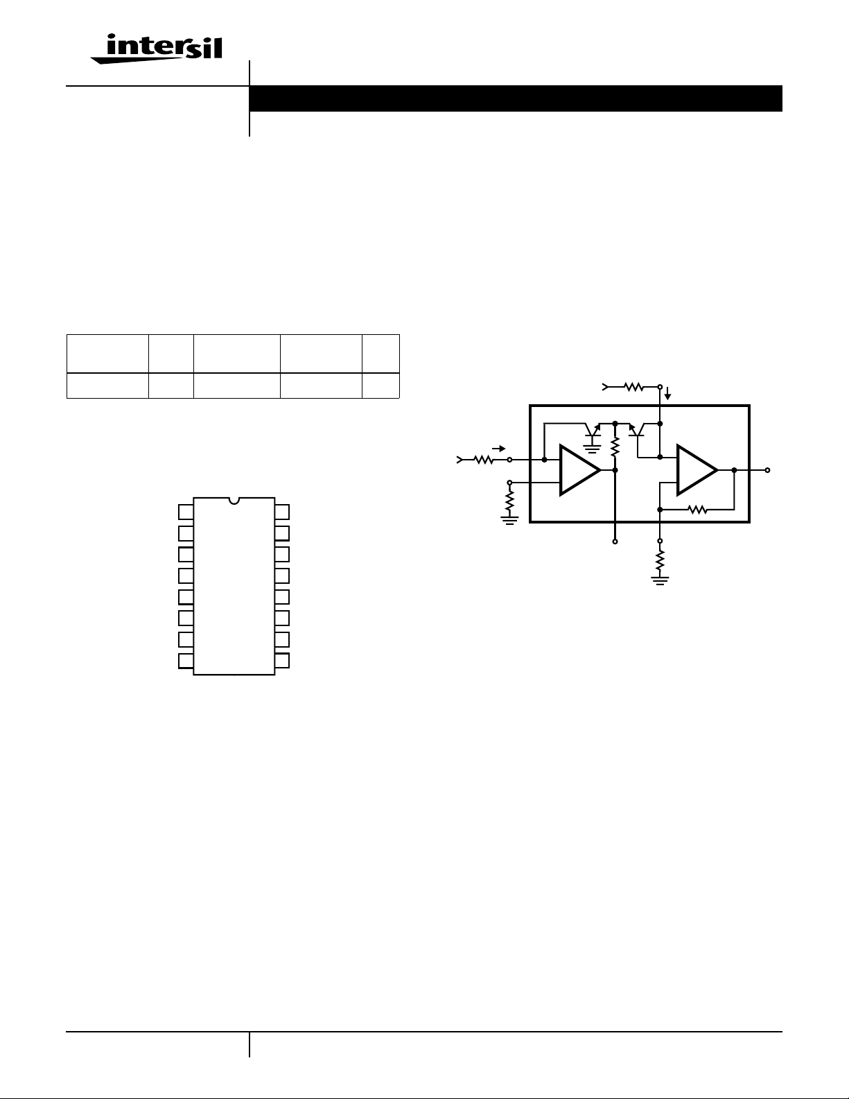
ICL8048
Data Sheet August 1999
Log Amplifier
The ICL8048 is a monolithic logarithmic amplifier capable of
handling six decades of current input, or three decades of
voltage input. It is fully temperature compensated and is
nominally designed to provide 1V of output for each decade
change of input. For increased flexibility, the scale factor,
reference current and offset voltage are externally
adjustable.
Ordering Information
PART
NUMBER
ICL8048BCJE 30mV 0 to 70 16 Ld CERDIP F16.3
ERROR
(25oC)
TEMPERA TURE
RANGE (oC) PACKAGE
PKG.
NO.
Pinout
ICL8048
(CERDIP)
TOP VIEW
File Number 2865.2
Features
• Full Scale Accuracy . . . . . . . . . . . . . . . . . . . . . . . . . 0.5%
o
• Temperature Compensated Operation. . . . . . 0
C to 70oC
• Scale Factor, Adjustable. . . . . . . . . . . . . . . . . 1V/Decade
• Dynamic Current Range. . . . . . . . . . . . . . . . . . . . . 120dB
• Dynamic Voltage Range. . . . . . . . . . . . . . . . . . . . . . 60dB
• Dual JFET Input Op Amps
Functional Diagram
ICL8048
V
REF
Q
f
V
IN
IN
GND
2
1
-
A
1
+
Q
1
I
REF
16
2
+
A
2
-
V
OUT
10
OFFSET
A
1
A
OFFSET
1
OUTPUT
A
1
GND
NC
NULL
NULL
NC
1
2
I
IN
3
4
5
6
V-
7
8
16
I
REF
7
15
GAIN
A
14
NC
A
OFFSET
2
13
NULL
OFFSET
A
2
12
NULL
11
V+
10
V
OUT
9
NC
OUTPUT
1
15
GAIN
1
CAUTION: These devices are sensitive to electrostatic discharge; follow proper IC Handling Procedures.
1-888-INTERSIL or 321-724-7143
| Copyright © Intersil Corporation 1999
Page 2
ICL8048
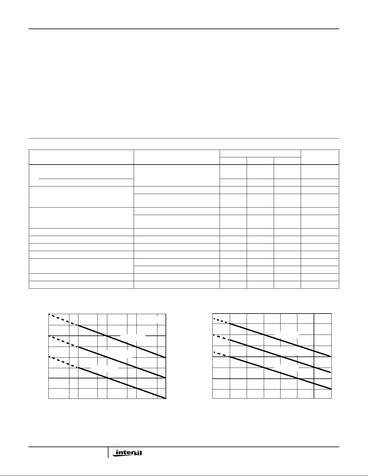
Absolute Maximum Ratings Thermal Information
Supply Voltage . . . . . . . . . . . . . . . . . . . . . . . . . . . . . . . . . . . . . . . . . ±18V
IIN (Input Current) . . . . . . . . . . . . . . . . . . . . . . . . . . . . . . . . . . . 2mA
I
(Reference Current). . . . . . . . . . . . . . . . . . . . . . . . . . . . . . 2mA
REF
Voltage Between Offset Null and V+ . . . . . . . . . . . . . . . . . . . . ±0.5V
Output Short Circuit Duration. . . . . . . . . . . . . . . . . . . . . . . Indefinite
Thermal Resistance (Typical, Note 1) θJA (oC/W) θJC (oC/W)
CERDIP Package. . . . . . . . . . . . . . . . . 75 22
Maximum Junction Temperature (Hermetic Package or Die) . . .175oC
Maximum Storage Temperature Range. . . . . . . . . . -65oC to 150oC
Maximum Lead Temperature (Soldering 10s) . . . . . . . . . . . . .300oC
Operating Conditions
Temperature Range . . . . . . . . . . . . . . . . . . . . . . . . . . . . 0oC to 70oC
CAUTION: Stresses above those listed in “Absolute Maximum Ratings” may cause permanent damage to the device. This is a stress only rating and operation of the
device at these or any other conditions above those indicated in the operational sections of this specification is not implied.
Die Characteristics
Number of Transistors or Gates. . . . . . . . . . . . . . . . . . . . . . . . . . . 62
NOTE:
1. θJA is measured with the component mounted on an evaluation PC board in free air.
Electrical Specifications V
= ±15V, TA = 25oC, I
S
= 1mA, Scale Factor Adjusted for 1V/Decade, Unless Otherwise Specified
REF
ICL4048BC
PARAMETER TEST CONDITIONS
UNITSMIN TYP MAX
Dynamic Range
(1nA - 1mA) RIN = 10kΩ 120 - - dB
I
IN
VIN (10mV - 10V) 60 - - dB
Error, % of Full Scale IIN = 1nA to 1mA - 0.20 0.5 %
TA = 0oC to 70oC,
- 0.60 1.25 %
IIN = 1nA to 1mA
Error, Absolute Value IIN = 1nA to 1mA - 12 30 mV
TA = 0oC to 70oC,
-3675 mV
IIN = 1nA to 1mA
Temperature Coefficient of V
OUT
IIN = 1nA to 1mA - 0.8 - mV/oC
Power Supply Rejection Ratio Referred to Output - 2.5 - mV/V
Offset Voltage (A1 and A2) Before Nulling - 15 25 mV
Wideband Noise At Output, for IIN = 100µA - 250 - µV
RMS
Output Voltage Swing RL = 10kΩ±12 ±14 - V
RL = 2kΩ±10 ±13 - V
Power Consumption - 150 200 mW
Supply Current - 5 6.7 mA
Typical Performance Curves
+4
+3
+2
+1
0
-1
OUTPUT VOLTAGE (V)
-2
-3
-4
1mV 10mV 100mV 1V 10V
I
= 100nA
REF
INPUT VOLTAGE (V)
I
REF
I
= 10µA
REF
RIN = 10kΩ
= 1mA
FIGURE 1. TRANSFER FUNCTION FOR VOLTAGE INPUTS FIGURE 2. TRANSFER FUNCTION FOR CURRENT INPUTS
2
+8
+6
+4
+2
0
-2
OUTPUT VOLTAGE (V)
-4
-6
-8
10
-10
I
= 1mA
REF
I
= 1µA
REF
I
= 1nA
REF
-9
-8
-7
-6
-5
10
10
10
10
10
INPUT CURRENT (A)
-4
10
-3
10
Page 3
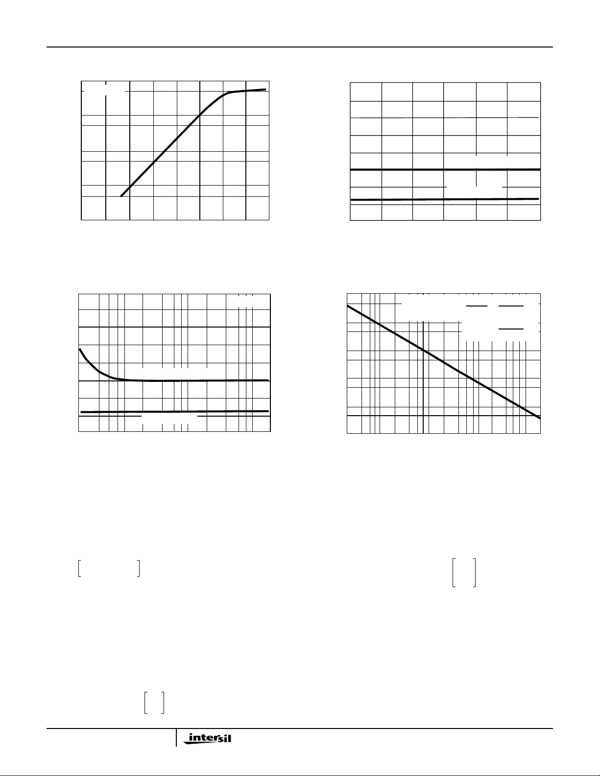
Typical Performance Curves (Continued)
ICL8048
100K
I
= 1mA
REF
10K
1K
100
SMALL SIGNAL BANDWIDTH (Hz)
10
-11
10
-9
10
INPUT CURRENT (A)
-7
10
-5
10
10
FIGURE 3. SMALL SIGNAL BANDWIDTHvs INPUT
CURRENT
200
175
150
125
100
75
50
25
MAXIMUM ERROR VOLTAGE (±mV)
0
10mV 100mV 1V 10V
8048BC (0oC TO 70oC)
8048BC (25oC)
INPUT VOLTAGE (V)
RIN = 10kΩ
FIGURE 5. MAXIMUM ERROR VOLTAGEAT THE OUTPUT vs
INPUT VOLTAGE
200
175
150
125
100
75
50
25
MAXIMUM ERROR VOLTAGE (±mV)
-3
0
-9
10
-8
10
-7
10
INPUT CURRENT (A)
8048BC (0oC TO 70oC)
8048BC (25oC)
-6
10
-5
10
-4
10
-3
10
FIGURE 4. MAXIMUM ERROR VOLTAGEAT THE OUTPUT vs
INPUT CURRENT
1000
434
100
10
1
VOLTAGE GAIN
0.1
0.01
1mV 10mV 100mV 1V 10V
R
= 10kΩ
IN
INPUT VOLTAGE (V)
∆V
∆V
IN
OUT
=VOLTAGE GAIN =
=
log10 e
V
IN
4343
V
IN
V
/
V
FIGURE 6. SMALL SIGNAL VOLTAGEGAIN vs INPUT
VOLTAGE FOR RS = 10kΩ
ICL8048 Detailed Description
The ICL8048 relies for its operation on the well known
exponential relationship between the collector current and
the base emitter voltage of a transistor:
ICISexp
---------------
kT
1–=
qV
B
E
For base emitter voltages greater than 100mV, Equation 1
becomes
qV
BE
ICISexp
=
--------------- -
kT
From Equation 2, it can be shown that for two identical
transistors operating at different collector currents, the V
difference (∆VBE) is given by:
∆V
BE
=
-2.303
kT
------ -
× log
q
10
I
C1
---------
I
C2
3
(EQ. 1)
(EQ. 2)
(EQ. 3)
BE
Referring to Figure 7 it is clear that the potential at the
collector of Q
output voltage is ∆V
V
=
OUT
The expression has a numerical value of 59mV at
o
25
C; thus in order to generate 1V/decade at the output, the
ratio (R
1+R2
is equal to the ∆VBEbetween Q1and Q2. The
2
-2.303
multiplied by the gain of A2:
BE
R1R2+
--------------------- -
2.303
kT
------ -
log
R
2
kT
------ -
×
q
10
q
I
IN
--------------
I
REF
)/R2is chosen to be 16.9. For this scale factor
(EQ. 4)
to hold constant as a function of temperature, the
(R
)/R2 term must have a 1/T characteristic to
1+R2
compensate for kT/q.
In the ICL8048 this is achieved by making R
a thin film
1
resistor, deposited on the monolithic chip. It has a nominal
value of 15.9kΩ at 25
o
C, and its temperature coefficient is
Page 4

ICL8048
V
V+
R
4
I
IN
V
IN
R
IN
GND
2
1
150pF
10kΩ
54
2kΩ
Q
-
A
+
C
1
R
0
1
1
OUTPUT
A
1
FIGURE 7. ICL8048 OFFSET AND SCALE FACTOR ADJUSTMENT
REF
R
7
(+15V)
R
REF
3
R
R
2kΩ
+
A
2
-
R
1
15.9kΩ
V+
5
V
OUT
10
I
REF
16
Q
2
GAIN
15
680Ω (LOW T.C.)
2
1kΩ
carefully designed to provide the necessary compensation.
Resistor R
is external and should be a low T.C. type; it
2
should have a nominal value of 1kΩ to provide 1V/decade,
and must have an adjustment range of ±20% to allow for
production variations in the absolute value of R
.
1
ICL8048 Offset and Scale Factor
Adjustment
A log amp, unlike an op amp, cannot be offset adjusted by
simply grounding the input. This is because the log of zero
approaches minus infinity; reducing the input current to zero
starves Q
around A
of A
of collector current and opens the feedback loop
1
. Instead, it is necessary to zero the offset voltage
1
and A2 separately, and then to adjust the scale factor.
1
Referring to Figure 7, this is done as follows:
1. Temporarily connect a 10kΩ resistor (R
and 7. With no input voltage, adjust R
A
(pin 7) is zero. Remove R0.
1
) between pins 2
0
until the output of
4
Note that fora current input, this adjustment is not necessary since the offset voltage of A
does not cause any er-
1
ror for current source inputs.
2. Set I
IN=IREF
=1mA.AdjustR5suchthattheoutputofA
(pin 10) is zero.
3. Set I
=1µA, I
IN
= 1mA. Adjust R2for V
REF
OUT
=3V(for
a 1V/decade scale factor) or 6V (for a 2V/decade scale
factor).
Step #3 determines the scale factor. Setting IIN = 1µA
optimizesthe scale factor adjustment over a fairly wide dynamic
range, from 1mA to 1nA. Clearly, if the ICL8048 is to be used
forinputs which only span the range 100µA to 1mA, it would be
better to set I
other scale factors would require different I
= 100µA in Step #3. Similarly, adjustment for
IN
and V
IN
OUT
values.
Applications Information
ICL8048 Scale Factor Adjustment
The scale factor adjustment procedures outlined previously
for the ICL8048, are primarily directed towards setting up 1V
(∆V
decade (∆V
) per decade (∆IIN or ∆VIN) for the log amp, or one
OUT
) per volt (∆VIN) for the antilog amp.
OUT
This corresponds to K = 1 in the respective transfer functions:
V
OUT
=
-K log
By adjusting R
IN
--------------
10
I
REF
(Figure 7) the scale factor “K” in Equation 5
2
(EQ. 5)
I
can be varied. The effect of changing K is shown graphically
in Figure 8 for the log amp. The nominal value of R
required
2
to give a specific value of K can be determined from
Equation 6. It should be remembered that R
has a ±20%
1
tolerance in absolute value, so that allowance shall be made
for adjusting the nominal value of R
941
-----------------------------
R
2
K 0.059–()
Ω=
by ±20%.
2
(EQ. 6)
ICL8048 Automatic Offset Nulling Circuit
The ICL8048 is fundamentally a logarithmic current
amplifier. It can be made to act as a voltage amplifier by
placing a resistor between the current input and the voltage
source but, since I
is accurate only when V
2
voltage. A substantial reduction of V
voltage operation over a 120dB range.
12
10
8
6
4
2
OUTPUT VOLTAGE (V)
0
-2
-1010-9
10
FIGURE 8. EFFECT OF VARYING “K” ON THE LOG AMPLIFIER
=(VIN-V
IN
IN
K = 0.5
-8
10
INPUT CURRENT (A)
OFFSET
)/RIN, this conversion
is much greater than the offset
would allow
I
REF
-5
10
10
= 1mA
-4
K = 1
10
OFFSET
K = 2
-7
-6
10
-3
10
4
Page 5

0.1µF
V
IN
1K
ICL8048
33kΩ
0.1µF
0V
-
ICL7650
+
R
IN
I
IN
V
OFFSET
0.1µF
V
33kΩ
45
2
(+15V)
Q
1
REF
-
A
1
+
C
1
150pF
1
A1 OUTPUT
R
REF
I
REF
Q
2
R
3
ICL8048
7
FIGURE 9. ICL8048 OFFSET NULLED BY ICL7650
16
+
-
GAIN
15
R
680Ω
(LOW T.C.)
R
5
2kΩ
12
A
2
R
1
15.9kΩ
2
13
1kΩ
V+
10
V
OUT
Figure 9 shows the ICL8048 in an automatic offset nulling
configuration using the ICL7650S. The extremely lo w offset
voltageof the ICL7650S forces its non-inverting input (and thus
pin 2 of the ICL8048) to the same potential as its inverting input
by nulling the first stage of the log amp. Since V
within a few µV of ground potential, R
can perform its voltage
IN
OFFSET
is now
to current conversion much more accurately, and without an
offset trimmer pot. Step 1 of the offset and scale factor
adjustment is eliminated, simplifying calibration.
NOTE: The ICL7650S op amp has a maximum supply voltage of
18V. The ICL8048 will operate at this voltage, but I
REF
must be
limited to 200µA or less for proper calibration and operation. Best
performance will be achieved when the ICL7650S has a ±3V to ±8V
supply and the ICL8048 is at its recommended ±15V supply. See
A053 for a method of powering the ICL7650S from a ±15V source.
Frequency Compensation
Although the op amps in the ICL8048 are compensated for
unity gain, some additional frequency compensation is
required. This is because the log transistors in the feedback
loop add to the loop gain. In the ICL8048, 150pF should be
connected between Pins 2 and 7 (Figure 7).
Error Analysis
Performing a meaningful error analysis of a circuit containing a
log and antilog amplifiers is more complex than dealing with a
similar circuit involving only op amps. In this data sheet e v ery
effort has been made to simplify the analysis task, without in
any way compromising the v alidity of the resultant n umbers.
The key difference in making error calculations in log/antilog
amps, compared with op amps, is that the gain of the former
is a function of the input signal level. Thus, it is necessary,
when referring errors from output to input, or vice versa, to
check the input voltage level, then determine the gain of the
circuit by referring to the graphs given in the Typical
Performance Curves section.
The various error terms in the log amplifier, the ICL8048, are
Referred To the Output (RTO) of the device. The errors are
expressed in this way because in the majority of systems a
number of log amps interface with an antilog amp, as shown
in Figure 10.
ERROR DUE TO A (RTO)
INPUT
INPUT ERROR DUE TO B (RTO)
LOG AMP
A
LOG AMP
B
= xmV
= ymV
ERROR DUE TO C (RTI)
= zmV
ANTI LOG
A
AMP
C
OUTPUT
FIGURE 10.
It is very straightforward to estimate the system error at node
(A) by taking the square root of the sum-of-the-squares of
the errors of each contributing block.
Total Error x2y2z
2
++at (A)=
If required, this error can be referred to the system output
through the voltage gain of the antilog circuit, using the
voltage gain versus input voltage plot.
The numerical values of x, y,and z in the above equation are
obtained from the maximum error voltage plots. For
example, with the ICL8048BC, the maximum error at the
output is 30mV at 25
o
C. This means that the measured
output will be within 30mV of the theoretical transfer
function, provided the unit has been adjusted per the
procedures described previously. Figure 11 illustrates this
point.
5
Page 6

ICL8048
8
6
4
2
0
-2
-4
OUTPUT VOLTAGE (V)
-6
-8
10
FIGURE 11. TRANSFER FUNCTION FOR CURRENT INPUTS
I
REF
-1010-910-810-710-610-510-410-3
INPUT CURRENT (A)
I
REF
= 1nA
I
REF
= 1µA
= 1mA
THEORETICAL
30mV
TRANSFER FN
30mV
Actual output will lie
within shaded area for
ICL8048BC at 25oC
To determine the maximum error over the operating
temperature range, the 0
o
C to 70oC absolute error values
given in the table of electrical specifications should be used.
For intermediate temperatures, assume a linear increase in
the error between the 25
o
C value and the 70oC value.
It is important to note that the ICL8048 requires positive
values of I
Application of negative I
, and the input current must also be positive.
REF
to the ICL8048 or negative I
IN
REF
will cause malfunction, and if maintained for long periods,
would lead to device degradation. Some protection can be
provided by placing a diode between pin 7 and ground.
Clearly it is possible to perform division using just one
ICL8048, followed by an antilog amplifier. For multiplication,
it is generally necessary to use two log amps, summing their
outputs into an antilog amp.
To avoid the problems caused by the I
input not being a
REF
true virtual ground (discussed in the previous section), the
circuit of Figure 12 is again recommended if the I
REF
input is
to be modulated.
Definition of Terms
In the definitions which follow, it will be noted that the various
error terms are referred to the output of the log amp, and to
the input of the antilog amp. The reason for this is explained
on the previous page.
Dynamic Range. The dynamic range of the ICL8048 refers
to the range of input voltages or currents over which the
device is guaranteed to operate.
Error, Absolute Value. The absolute error is a measure of
the deviation from the theoretical transfer function, after
performing the offset and scale factor adjustments as
outlined, (ICL8048). It is expressed in mV and referred to the
linear axis of the transfer function plot. Thus, in the case of
the ICL8048, it is a measure of the deviation from the
theoretical output voltage for a given input current or voltage.
Setting Up the Reference Current
The input current reference pin (I
ground. For the ICL8048, a fraction of the output voltage is
seen on Pin 16 (Figure 7). This does not constitute an
appreciable error provided V
REF
voltage. A 10V or 15V reference satisfies this condition.
Alternatively, I
can be provided from a true current
REF
source. One method of implementing such a current source
is shown in Figure 12.
+15V
-
V
REF
I
REF
741
+
= V
REF/R1
(TO PIN 16 ON ICL8048)
FIGURE 12.
) is not a true virtual
REF
is much greater than this
+15V
R
1
2N2609
2N2219
10kΩ
I
REF
Log of Ratio Circuit, Division
The ICL8048 may be used to generate the log of a ratio by
modulating the I
same, as defined by Equation 7:
V
OUT
Klog–
=
input. The transfer function remains the
REF
I
IN
--------------
10
I
REF
(EQ. 7)
The absolute error specification is guaranteed over the
dynamic range.
Error, % of Full Scale. The error as a percentage of full
scale can be obtained from the following relationship:
Error, % of Full Scale
Temperature Coefficient of V
100 Error, absolute value×
-----------------------------------------------------------------------=
Full Scale Output Voltage
. For the ICL8048 the
OUT
temperature coefficient refers to the drift with temperature of
V
for a constant input current.
OUT
Power Supply Rejection Ratio. The ratio of the voltage
change in the linear axis of the transfer function (V
OUT
for
the ICL8048) to the change in the supply voltage, assuming
that the log axis is held constant.
Wideband Noise. For the ICL8048, this is the noise
occurring at the output under the specified conditions.
Scale Factor. For the log amp, the scale factor (K) is the
voltage change at the output for a decade (i.e., 10:1) change
at the input. See Equation 5.
Application Notes
For further applications assistance, see A007 “The
ICL8048/8049 Monolithic Log-Antilog Amplifiers”.
6
Page 7

ICL8048
Ceramic Dual-In-Line Frit Seal Packages (CERDIP)
LEAD FINISH
c1
-A-
-B-
bbb C A - B
S
BASE
PLANE
SEATING
PLANE
S1
b2
b
ccc C A - BMD
D
A
A
e
S
S
NOTES:
1. Index area: A notch ora pin one identification markshallbe located adjacent to pin one and shall be located within the shaded
area shown. The manufacturer’s identification shall not be used
as a pin one identification mark.
2. The maximum limits of lead dimensions b and c or M shall be
measured at the centroid of the finished lead surfaces, when
solder dip or tin plate lead finish is applied.
3. Dimensions b1 and c1 apply to lead base metal only. Dimension
M applies to lead plating and finish thickness.
4. Corner leads (1, N, N/2, and N/2+1) may be configured with a
partial lead paddle. For this configuration dimension b3 replaces
dimension b2.
5. This dimension allows for off-center lid, meniscus, and glass
overrun.
6. Dimension Q shall be measured from the seating plane to the
base plane.
7. Measure dimension S1 at all four corners.
8. N is the maximum number of terminal positions.
9. Dimensioning and tolerancing per ANSI Y14.5M - 1982.
10. Controlling dimension: INCH.
-DBASE
E
D
S
S
Q
A
-CL
METAL
b1
M
(b)
SECTION A-A
α
(c)
M
eA
eA/2
aaa C A - B
M
c
D
S S
F16.3 MIL-STD-1835 GDIP1-T16 (D-2, CONFIGURATION A)
16 LEAD CERAMIC DUAL-IN-LINE FRIT SEAL PACKAGE
INCHES MILLIMETERS
SYMBOL
A - 0.200 - 5.08 -
b 0.014 0.026 0.36 0.66 2
b1 0.014 0.023 0.36 0.58 3
b2 0.045 0.065 1.14 1.65 b3 0.023 0.045 0.58 1.14 4
c 0.008 0.018 0.20 0.46 2
c1 0.008 0.015 0.20 0.38 3
D - 0.840 - 21.34 5
E 0.220 0.310 5.59 7.87 5
e 0.100 BSC 2.54 BSC -
eA 0.300 BSC 7.62 BSC -
eA/2 0.150 BSC 3.81 BSC -
L 0.125 0.200 3.18 5.08 -
Q 0.015 0.060 0.38 1.52 6
S1 0.005 - 0.13 - 7
o
α
90
105
o
90
o
105
aaa - 0.015 - 0.38 bbb - 0.030 - 0.76 -
ccc - 0.010 - 0.25 -
M - 0.0015 - 0.038 2, 3
N16 168
NOTESMIN MAX MIN MAX
o
Rev. 0 4/94
-
All Intersil semiconductor products are manufactured, assembled and tested under ISO9000 quality systems certification.
Intersil semiconductor products are sold by description only.Intersil Corporation reserves the right to make changes in circuit design and/or specifications at any time without notice. Accordingly, the reader is cautioned to verify that data sheets are current before placing orders. Information furnished by Intersil is believed to be accurate and
reliable. However, no responsibility is assumed by Intersil or its subsidiaries for its use; nor for any infringements of patents or other rights of third parties which may result
from its use. No license is granted by implication or otherwise under any patent or patent rights of Intersil or its subsidiaries.
For information regarding Intersil Corporation and its products, see web site www.intersil.com
Sales Office Headquarters
NORTH AMERICA
Intersil Corporation
P. O. Box 883, Mail Stop 53-204
Melbourne, FL 32902
TEL: (321) 724-7000
FAX: (321) 724-7240
7
EUROPE
Intersil SA
Mercure Center
100, Rue de la Fusee
1130 Brussels, Belgium
TEL: (32) 2.724.2111
FAX: (32) 2.724.22.05
ASIA
Intersil (Taiwan) Ltd.
7F-6, No. 101 Fu Hsing North Road
Taipei, Taiwan
Republic of China
TEL: (886) 2 2716 9310
FAX: (886) 2 2715 3029
 Loading...