

Datasheet ICL7663SACBA, ICL7663SACPA, ICL7663SAIPA, ICL7663SCPA Datasheet (Intersil Corporation)
Page 1
TM
ICL7663S
Data Sheet April 1999
CMOS Programmable Micropower
Positive Voltage Regulator
The ICL7663S Super Programmable Micropower Voltage
Regulator is a low power, high efficiency positive voltage
regulator which accepts 1.6V to 16V inputs and provides
adjustable outputs from 1.3V to 16V at currents up to 40mA.
It is a direct replacem ent for the industry stan dard ICL7663B
offering wider operating voltage and temper ature ranges,
improved output acc uracy ( ICL7663SA) , better t empera ture
coefficient, guaranteed maximum supply current, and
guaranteed line and load regulation. All improvements are
highlighted in the electrical characteristics section. Critical
parameters ar e guaranteed over the entire commercial
and industrial temperature ranges. The ICL7663S/SA
programmable out put voltage is set by two ext ernal resist ors.
The 1% referen ce a ccuracy of the I CL766 3SA eli minates the
need for trimming the output voltage in most applications.
The ICL7663S is well suit ed for battery powered supplies,
featuring 4µA quiesce nt current , low V
output curren t sensing and logic input level shutdown
control. In addi tion, the ICL7663S has a negative
temperature coefficient output sui table for generating a
temperature compensated display drive voltage for LCD
displays.
IN
to V
differential ,
OUT
File Number 3180.3
Features
• Guaranteed 10µA Maximum Quiescent Current Over All
Temperature Ranges
• Wider Operati ng Voltage Range - 1.6V to 16V
• Guaranteed Line and Load Regulation Over Entire
Operating Temperat ure Range Optional
• 1% Output Voltage Accuracy (ICL7663SA)
• Output Voltage Programmable from 1.3V to 16V
• Improved Temperature Coefficient of Output Voltage
• 40mA Minimum Output Current with Current Limiting
• Output Voltages with Programmable Negative
Temperature Coefficients
• Output Shutdown via Current-Limit Sensing or External
Logic Level
• Low Input-to-Output Voltage Differential
• Improved Direct Replacement for Industry Standard
ICL7663B and Other Second-Source Products
Applications
• Low-Power Portable Inst rumentation
• Pagers
Ordering Information
TEMP. RANGE
PART NUMBER
ICL7663SCBA 0
ICL7663SCPA 0 to 70 8 Ld PDIP E8.3
ICL7663SACBA 0
ICL7663SACPA 0
ICL7663SIBA -25 to 85 8 Ld SOIC (N) M8.15
ICL7663SIPA -25
ICL7663SAIBA -25
ICL7663SAIPA -25 to 85 8 Ld PDIP E8.3
(oC) PACKAGE PKG. NO.
to 70 8 Ld SOIC (N) M8.15
to 70 8 Ld SOIC (N) M8.15
to 70 8 Ld PDIP E8.3
to 85 8 Ld PDIP E8.3
to 85 8 Ld SOIC (N) M8.15
• Handheld Inst ruments
• LCD Display Modules
• Remote Data Loggers
• Battery-Powered Systems
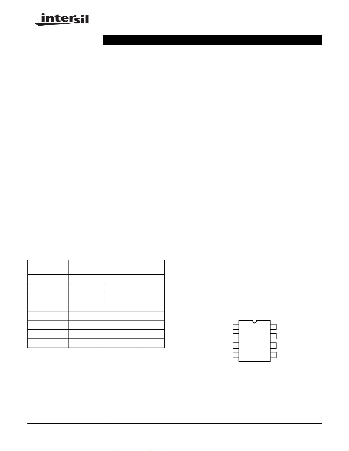
Pinout
ICL7663S
(PDIP, CERDIP, SOIC)
TOP VIEW
V
V
OUT2
OUT1
GND
1
2
3
4
SENSE
8
7
6
5
VIN+
V
TC
V
SET
SHDN
55
CAUTION: These devices are sensitive to electrostatic discharge; follow proper IC Handling Procedures.
1-888-INTERSIL or 321-724-7143
| Intersil (and design) is a trademark of Intersil Americas Inc.
Copyright © Intersil Americas Inc. 2001. All Rights Reserved
Page 2
ICL7663S
Absolute Maximum Ratings Thermal Information
Input Supply Voltage . . . . . . . . . . . . . . . . . . . . . . . . . . . . . . . . .+18V
Any Input or Output Voltage (Note 1 )
Terminal s 1, 2, 3, 5, 6, 7. . . . . . . . . . . . . V
+ 0.3V to GND -0.3V
IN
Output Source Current
Terminal 2 . . . . . . . . . . . . . . . . . . . . . . . . . . . . . . . . . . . . . . 50mA
Terminal 3 . . . . . . . . . . . . . . . . . . . . . . . . . . . . . . . . . . . . . . 25mA
Output Sinking Current
Terminal 7 . . . . . . . . . . . . . . . . . . . . . . . . . . . . . . . . . . . . . -10mA
Operating C o ndi t io ns
Temperature R an ge
ICL7663SC. . . . . . . . . . . . . . . . . . . . . . . . . . . . . . . . . 0
ICL7663SI . . . . . . . . . . . . . . . . . . . . . . . . . . . . . . . -25
CAUTION: Stress es abov e thos e lis ted in “ A bsolute Max imum R a tings” ma y cause per manen t dam age to th e de vice. This is a s tress on ly rating and ope rat ion of th e
device at these or any other conditions above those indicated in the operational sections of this specification is not implied.
NOTES:
1. Connecting any terminal to voltages greater than (V+
mended that no inputs from s ources ope rating on external power supplies be applied prior to ICL7663S power-up.
is measured with the componen t mounted on an evaluation PC board in free air.
2. θ
JA
o
C to 70oC
o
C to 85oC
+ 0.3V) or less than (GND - 0.3V) may cause destructive device latch-up. It is recom-
IN
Thermal Resistance (Typical, Note 2) θ
(oC/W) θJC (oC/W)
JA
CERDIP Package. . . . . . . . . . . . . . . . . 115 30
PDIP Package . . . . . . . . . . . . . . . . . . . 150 N/A
Plastic SOIC Package . . . . . . . . . . . . . 180 N/A
Maximum Junction Temperature
PDIP Package . . . . . . . . . . . . . . . . . . . . . . . . . . . . . . . . . 150
CERDIP Package. . . . . . . . . . . . . . . . . . . . . . . . . . . . . . . 175
Maximum Storage Temperature Range . . . . . . . . . -65
o
C to 150oC
Maximum Lead Temperature (Soldering 10s) . . . . . . . . . . . . .300
(SOIC - Lead Tips On ly)
o
C
o
C
o
C
Electrical Specifications Specifications B elow Applicable to Both ICL7663S and IC L7663SA, Unless Otherwi se Specified. V+
V
= 5V, TA = 25oC, Unless Otherwise Specified. Notes 4, 5. See Test Circ uit, Figure 7
OUT
PARAMETER SYMBOL TEST CONDITIONS MIN TYP MAX UNITS
Input Voltage V+
Quie sc en t C urr e nt I
Refere nce Volta ge V
Temperature
∆V
Coefficient
Line Regulation ∆V
V
SET’
V
Input Current I
SET
Shutdown Input Current I
Shutdown Input Voltage V
Sense Pin Input Current I
SHDN
SHDN
SENSE
Sense Pin Input Threshold V
SET
∆T
SET
ICL7663S TA = 25oC1.5-16V
IN
o
0
C < TA < 70oC1.6-16V
-25oC < TA < 85oC1.6- 16V
ICL7663SA 0
1.4V ≤ V
Q
V+
≤ 8.5V, No Load
OUT
= 9V 0oC < TA < 70oC--10µA
IN
o
C < TA < 70oC1.6-16V
o
-25
C < TA < 85oC1.6- 16V
o
-25
C < TA < 85oC--10µA
V+IN = 16V 0oC < TA < 70oC--12µA
o
-25
C < TA < 85oC--12µA
I
OUT1
= 100µA, V
OUT
= V
SET
ICL7663S TA = 25oC 1.2 1.3 1.4 V
SET
ICL7663SA T
o
0
C < TA < 70oC - 100 - ppm
= 25oC 1.275 1.29 1.305 V
A
-25oC < TA < 85oC - 100 - ppm
2V < VIN < 15V 0oC < TA < 70oC-0.03-%/V
SET
∆V
IN
o
-25
C < TA < 85oC - 0.03 0.3 %/V
0oC < TA < 70oC - 0.01 10 nA
o
-25
C < TA < 85oC - 0.01 10 nA
- ±0.01 10 nA
V
SHDN
V
SHDN
HI: Both V
LO: Both V
Disabled 1.4 - - V
OUT
Enable - - 0.3 V
OUT
-0.0110nA
CL
-0.5- V
= 9V,
IN
56
Page 3
ICL7663S
Electrical Specifications Specifications B elow Applicable to Both ICL7663S and IC L7663SA, Unless Otherwi se Specified. V+
V
= 5V, TA = 25oC, Unless Otherwise Specified. Notes 4, 5. See Test Circ uit, Figure 7 (Continued)
OUT
= 9V,
IN
PARAMETER SYMBOL TEST CONDITIONS MIN TYP MAX UNITS
Input-Outp ut Sat ura ti on
Resistance (Note 3)
Load Regulation ∆V
Available Output Current
(V
)
OUT2
Negative Tempco Output
(Note 4)
Temperature Coeff icient ∆V
R
SAT
OUT
∆I
OUT
I
OUT2
V
TC
I
TC
V+IN = 2V, I
V+IN = 9V, I
V+
= 15V, I
IN
1mA < I
OUT2
50µA < I
OUT1
3V ≤ VIN ≤ 16V, VIN - V
= 1mA - 170 350 Ω
OUT1
= 2mA - 50 100 Ω
OUT1
= 5mA - 35 70 Ω
OUT1
< 20mA - 1 3 Ω
< 5mA - 2 10 Ω
= 1.5V 40 - - mA
OUT2
Open Circ ui t Volt age - 0.9 - V
Maximum Sink Current 0 8 2.0 mA
Open Circuit - +2.5 - mV/
TC
∆T
Minimum Load Current I
L(MIN)
Includes V
Divider TA = 25oC--1.0µA
SET
0oC < TA < 70oC-0.25.0µA
o
-25
C < TA < 85oC-0.25.0µA
NOTES:
3. This parameter refers to the saturation resistance of the MOS pass transistor. The minimum input-output voltage differential at low curre nt (u nder
5mA), can be determined by multiplying the load current (including set resist or curren t, but not quiescent current) by this resistance.
4. This output has a positive temperature coefficient. Using it in combination with the inverting input of the regul ator at V
coefficient results in the output voltage. See Figure 9 for details. Pin will not source current.
, a negative
SET
5. All pins are designed to withstand electrostatic discharge (ESD) levels in excess of 2000V.
6. All significant improvements over the industry standard IC L7663 are highlighted.
o
C
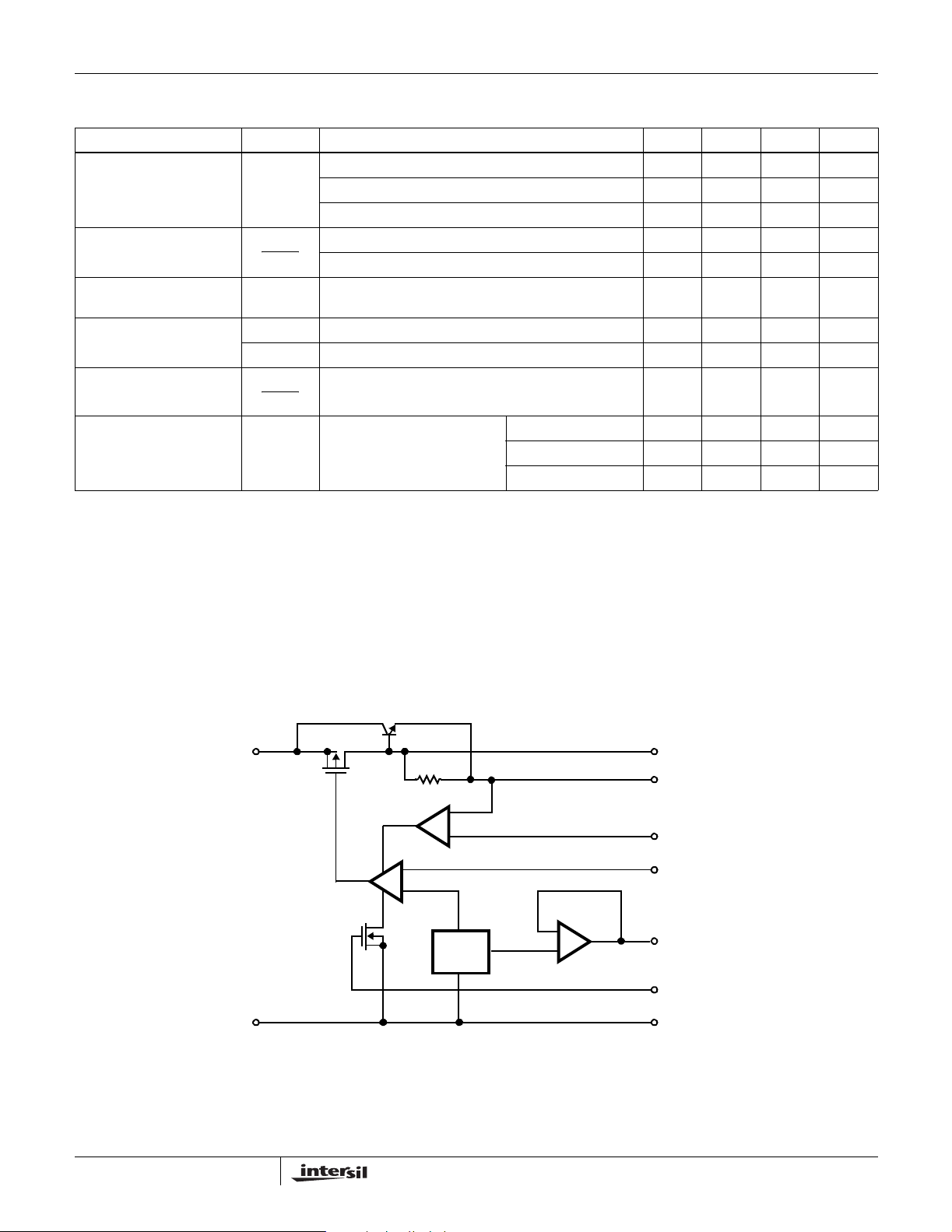
Functional Diagram
V+
GND
8
IN
C
A
REF
B
3
V
2
V
1
SENSE
6
V
7
V
5
SHUTDOWN
4
GND
OUT1
OUT2
SET
TC
57
Page 4

Typical Performance Curves
5.000
4.995
4.990
4.985
4.980
(V)
4.975
OUT
V
4.970
4.965
4.960
4.955
4.950
-3
10
-2
10
TA = 25oC
V+ = 9.0V
-1
10
I
(mA)
OUT
10
ICL7663S
2.0
1.8
1.6
1.4
1.2
1 (V)
1.0
OUT
- V
0.8
IN
V+
0.6
0.4
0.2
0
10
1
2
10
0
02468101214161820
V+IN = 2V
V+IN = 9V
I
OUT1
TA = 25oC
V+IN = 15V
(mA)
FIGURE 1. V
2.0
1.8
1.6
1.4
1.2
1 (V)
OUT
1.0
- V
0.8
IN
V+
0.6
0.4
0.2
0
0 5 10 15 20 25 30 35 40 45 50
FIGURE 3. V
OUTPUT VOLTAGE AS A FUNCTION OF
OUT2
OUTPUT CURRENT
TA = 25oC
V+IN = 2V
V+IN = 9V
V+IN = 15V
I
(mA)
OUT2
INPUT-OUTPUT DIFFERENTIAL vs
OUT2
OUTPUT CURRENT
5.0
4.5
4.0
3.5
3.0
2.5
(µA)
O
I
2.0
1.5
1.0
0.5
0
0246810121416
TA = -20oC
TA = -25oC
TA = -70oC
V+
(V)
IN
FIGURE 2. V
100
90
80
70
60
50
PSRR (dB)
40
30
20
10
0
-2
10
INPUT-OUTPUT DIFFERENTIAL vs
OUT1
OUTPUT CURRENT
VIN = 9.0V
= 2V
∆V
IN
-1
10
0
10
FREQUENCY (Hz)
10
1
2
10
FIGURE 4. NPUT POWER SUPPLY REJECTION RATIO
5.00
4.75
4.50
4.25
4.00
3.75
(µA)
O
I
3.50
3.25
3.00
2.75
2.50
-20 0 20 40 60 80
V+ = 15V
V+ = 2V
TEMPERATURE (
V+ = 9V
o
C)
1k
FIGURE 5. QUIESCENT CURRENT AS A FUNCTION OF
INPUT VOLTAGE
58
FIGURE 6. QUIESCENT CURRENT AS A FUNCTION OF
TEMPERATURE
Page 5

ICL7663S
Detailed Description
The ICL7663S is a CMO S integrated circui t i ncorporating all
the functions of a voltage regulator plus protection circuitry
on a single monolithic chip. Referring to the Funct ional
Diagram, the main blocks are a bandgap-type voltage
reference, an error amplifier, and an output driver with both
PMOS and NPN pass transistors.
The bandgap output voltage, trimmed to 1.29V ±15mV for
the ICL7663SA, and the input voltage at the V
SET
terminal
are compared in amplifier A. Error amplifier A drive s a
P-channel pass transistor which is sufficient for low (under
about 5mA) currents. The high current output is passed by
an NPN bipolar transistor connected as a follower. This
configuration gives more gain and lower output impedance.
Logic-controlled shutdown is implement ed via a N-Channel
MOS transistor. Curr ent-sensing is achieved with
comparator C, which functions with the V
ICL7663S has an output (V
) from a buffer amplifier ( B),
TC
terminal. The
OUT2
which can be used in combina ti on wit h am plifier A to
generate progr am ma ble-temperature-coefficient output
voltages.
The amplifi er, reference and co mp arat or circuitry al l operate
at bias levels well below 1µA to achieve extremely low
quiescent current. This does limit the dynamic response of
the circuits, however, and transients are best dealt with
outside the regulator loop.
Basic Operation
The ICL7663S is desi gned to regul ate bat tery v oltage s i n the
5V to 15V region at maximum load currents of about 5mA to
30mA. Although intended as low power devices, power
dissipation limits must b e observed. For exampl e, the power
dissipation in the case of a 10V supply regula ted down to 2V
with a load current of 30mA clearly exceeds the power
dissipation rating of the Mini-DIP:
-3
(10 - 2) (30) (10
The circuit of Figu re 8 il lustrates proper use of the device.
CMOS devices generally require two precautions: every
input pin must go somewher e, and maximum values of
applied voltages and current limits must be rigorously
observed. Negle cti ng these precautions may l ead to, at the
least, incorrect or nonoperation, and at worst, destructive
device failure. To avoid the problem of la tchup, do not apply
inputs to any pins before supply voltage is applied.
Input Voltages - The ICL7663S accepts working inputs of
1.5V to 16V. When power is applied, the rate-of-rise of the
input may be hundreds of volts per microsecond. This is
potentially harmful to the regulators, where internal
operating cur rents are in the nanoampere range. The
0.047µF capacitor on the device side of the switch will limit
inputs to a safe level around 2V/µs. Use of this capacitor is
suggested in all applications. In sever e rat e-of-rise cases, it
) = 240mW
may be advisable to use an RC network on th e SHutDowN
pin to delay output turn-on. Battery charging surges,
transients, and assorted noise signals should be kept from
the regulators by RC filt ering, zener protection, or even
fusing.
SENSE
V
OUT2
V
OUT1
V
GND
+
M
I
Q
OUT1
and V
TC
V
SET
SHDN
S
, open S2 for V
.
OUT2
0.047µF
+
-
NOTES:
when closed disables output current limiting.
7. S
1
8. Clos e S
9. IQ quiescent currents measured at GND pin by meter M.
10. S
both V
for V
2
when ON, per mi ts nor m al oper ati on, whe n OF F, sh ut s do wn
3
OUT1
FIGURE 7. ICL7663S TEST CIRCUIT
Output Voltages - The resistor divider R
scale the reference voltage, V
using the formula V
= (1 + R2/R1) V
OUT
R
CL
S
S
3
1
2
(7663 ONLY)
ON
OFF
1MΩ
OUT2
, to the desired output
SET
1.4V < V
.
2/R1
SET
V
OUT
R
2
R
L
R
1
1µA MIN
SHDN
is used to
. Suitable
< V+
C
L
IN
arrangements of these resistors, using a potentiometer,
enables exact val ues for V
to be obtained. In most
OUT
applications the potentiometer may be eliminated by using
the ICL7663SA. The ICL76 63SA has V
SET
voltage
guaranteed to be 1.29V ±15mV and when used with ±1%
tolerance res istors for R
and R2 the initial output voltage
1
will be within ±2.7% of ideal.
The low leakage cur rent of the V
to be tens of megohms for minimum additional q uiescent
R
2
terminal allows R1 and
SET
drain current. However, some load current is requi red for
proper operation, so for ext remely l ow-drai n appli catio ns it is
necessary to draw at least 1µA. This can include the curren t
and R1.
for R
2
Output volt ages up to near ly th e V
supply may b e obtai ned
IN
at low load currents , whi le t he low l imi t is the reference
voltage. The minimum input-output differential in each
regulator is obtained using the V
output differential increases to 1.5V when using V
, termin al . The i n put-
OUT1
OUT2
.
Output Currents - Low ou tput cu rrent s of le ss than 5m A are
obtained with the le ast input-output differ ential from the
terminal (connect V
V
OUT1
currents are nee ded, use V
OUT2
OUT2
to V
(V
). Where higher
OUT1
, should be left
OUT1
open in this case).
59
Page 6

V
W
V
T
ICL7663S
High output currents can be obtained only as far as package
dissipation allows. It is strongly re com m ended that output
current-limit sensing be used in such cases.
Current-Limit Sensing - The on-chip comparator (C in the
Functional Diagram) permits shutdown of the regulator
output in the event of excessive current drain. As Figure 8
shows, a current-limiting resistor, R
with V
load side of R
and the SENSE terminal is connected to the
OUT2
. When the current through RCL is high
CL
enough to produce a voltage drop equal to V
, is placed in series
CL
(0.5V) the
CL
voltage feedback is by-passed and the regulator output will
be limite d to t his c urrent . Ther efore, wh en the maximum load
current ( I
obtain the value for R
V
IN
=
OUT
=
I
CL
FIGURE 8. POSITIVE REGULATOR WITH CURRENT LIMIT
) is dete rmined, sim ply d ivide VCL by I
LOAD
R
2
V
R
+ R
R
1
CL
CL
0.047µF
1
= 25mA
V
SET
CL
V+
GND
.
IN
= 5V
SENSE
V
OUT2
V
OUT1
V
TC
V
SET
SHDN
20Ω
R
CL
604kΩ
210kΩ
to
LOAD
R
2
10µF
V
OUT
C
L
+5V
R
1
the regulated output volt age rea ches 90% of it s final val ue in
20ms. From:
I =∆VC ,C∆t=
I
OUT
(20 x 10-3)
0.9V
OUT
= 0.022
I
OUT
V
OUT
In addition, wher e such a c apaci tor is used, a cur rent- limit ing
resistor is also suggested (see “Current -Limit Sensing”).
Producing Output Voltages with Negative Temperature
Coefficients -The ICL7663S has an additional output which
o
is 0.9V relati ve to GND and has a tempco of +2.5mV/
C. By
applying t his voltage to the inverting input of amplifier A (i.e .,
the V
pin), output voltages having negative TC may be
SET
produced. The TC of the output voltage is controlled by the
R
ratio (see Figure 9 and its design equations).
2/R3
EQ. 1: V
OUT
EQ. 2: TC V
here:V
SET
= 0.9V
TC
+
V
TC
-
= V
SET
OUT
= 1.3V
R
1
R
3
=
V
SET
( R
1 +
-
R
2
-
+
+
V
REF
-
) R
2
+
R
R
2
R
3
R
1
(TC VTC) in mV/oC
V
OUT
2
(V
- VTC)
SET
3
CVTC = +2.5mV/oC
FIGURE 9. GENERATING NEGATIVE TEMPERATURE
COEFFICIENTS
Logic-Controllable Shutdown - When equipment is not
needed continuously (e.g., in remote data-acquisition
systems), it is desirable to eliminate its drain on the system
until it is required. This usually means switches, with their
unreliable contacts. Instead, the ICL7663S can be shut
down by a logic signal, leaving only I
(under 4µA) as a
Q
drain on the power source. Since this pin must not be left
open, it should be tied to ground if not needed. A voltage of
less than 0.3V for the ICL 7663S will keep the regulator ON,
and a voltage level of more than 1.4V but less t han V+
IN
will
turn the outputs OF F. If there is a possibility that the control
signal could exceed the regulator input (V+
) the current
IN
from this signal should be limited to 100µA maximum by a
high value (1MΩ) seri es resistor. This sit uati on may occur
when the logic signal originates from a system powered
separately from that of the regulator.
Additional Circuit Precautions - This regulator has poor
rejectio n of vol tage fluctuations fr om AC sources above
10Hz or so. To prevent the output from responding (where
this might be a problem), a reservoir capacitor across the
load is advi sed. The value of this capacitor is chosen so t hat
60
Applications
Boosting Output Current with External Transistor
The maximum availabl e output cu rrent from the ICL76 63S is
40mA. To obtain output currents greater than 40mA, an
external NPN transistor is used connected as shown in
Figure 10.
V
V+
OUT1
IN
V
IN
10µF
SENSE
GND
V
OUT2
V
SET
SHDN
100Ω
FIGURE 10. BOOSTING OUTPUT CURRENT WITH EXTERNAL
TRANSISTOR
EXTERNAL PIN
POWER
TRANSISTOR
0.47Ω
604kΩ
210kΩ
V
OUT
+5V
Page 7

ICL7663S
Generating a Temperature Compensa ted Display Drive Voltage
Temperature has an important effect in the variation of
threshold voltage in multiplexed LCD displays. As
temperaturerises, the threshold voltage goes down. For
applications where the display temperat ure varies widely, a
+5V
V+
LOGIC
SYSTEM,
PROCESSOR,
ETC.
ICL7663S
IN
V
OUT1
V
OUT2
V
temperature compensated display voltage, V
generated using the ICL7663S. This is shown in Figure 11
for the ICM7233 tripl exed LCD display driver.
1.8MΩ
SET
300kΩ
V
TC
V+
ICM7233
DISP
, can be
GND
DATA BUS
2.7MΩ
V
DISP
GND
GND
FIGURE 11. GENERATING A MULTIPLEXED LCD DISPLAY DRIVE VOLTAGE
61
 Loading...