

Page 1
ICL7663S
Data Sheet April 1999
CMOS Programmable Micropower
Positive Voltage Regulator
The ICL7663S Super Programmable Micropower Voltage
Regulator is a low power, high efficiency positive voltage
regulator which accepts 1.6V to 16V inputs and provides
adjustable outputs from 1.3V to 16V at currents up to 40mA.
It is a direct replacement for the industry standard ICL7663B
offering
improved
coefficient,
guaranteed line and load regulation. All improvements are
highlighted in the electrical characteristics section.
parameters are guaranteed over the entire commercial
and industrial temperature ranges.
programmableoutputvoltageis set bytwo external resistors.
The 1% reference accuracy of the ICL7663SA eliminates the
need for trimming the output voltage in most applications.
The ICL7663S is well suited for battery powered supplies,
featuring 4µA quiescent current, low V
output current sensing and logic input level shutdown
control. In addition, the ICL7663S has a negative
temperature coefficient output suitable for generating a
temperature compensated display drive voltage for LCD
displays.
wider
operating voltage and temperature ranges,
output accuracy (ICL7663SA), bettertemperature
guaranteed
maximum supply current, and
Critical
The ICL7663S/SA
IN
to V
OUT
differential,
File Number
3180.3
Features
•
Guaranteed
10µA Maximum Quiescent Current Over
Temperature Ranges
Wider
•
•
Operating Voltage Range - 1.6V to 16V
Guaranteed
Operating Temperature Range
Line and Load Regulation Over
Optional
Entire
• 1% Output Voltage Accuracy (ICL7663SA)
• Output Voltage Programmable from 1.3V to 16V
Improved
•
Temperature Coefficient of Output Voltage
• 40mA Minimum Output Current with Current Limiting
• Output Voltages with Programmable Negative
Temperature Coefficients
• Output Shutdown via Current-Limit Sensing or External
Logic Level
• Low Input-to-Output Voltage Differential
• Improved Direct Replacement for Industry Standard
ICL7663B and Other Second-Source Products
Applications
• Low-Power Portable Instrumentation
• Pagers
All
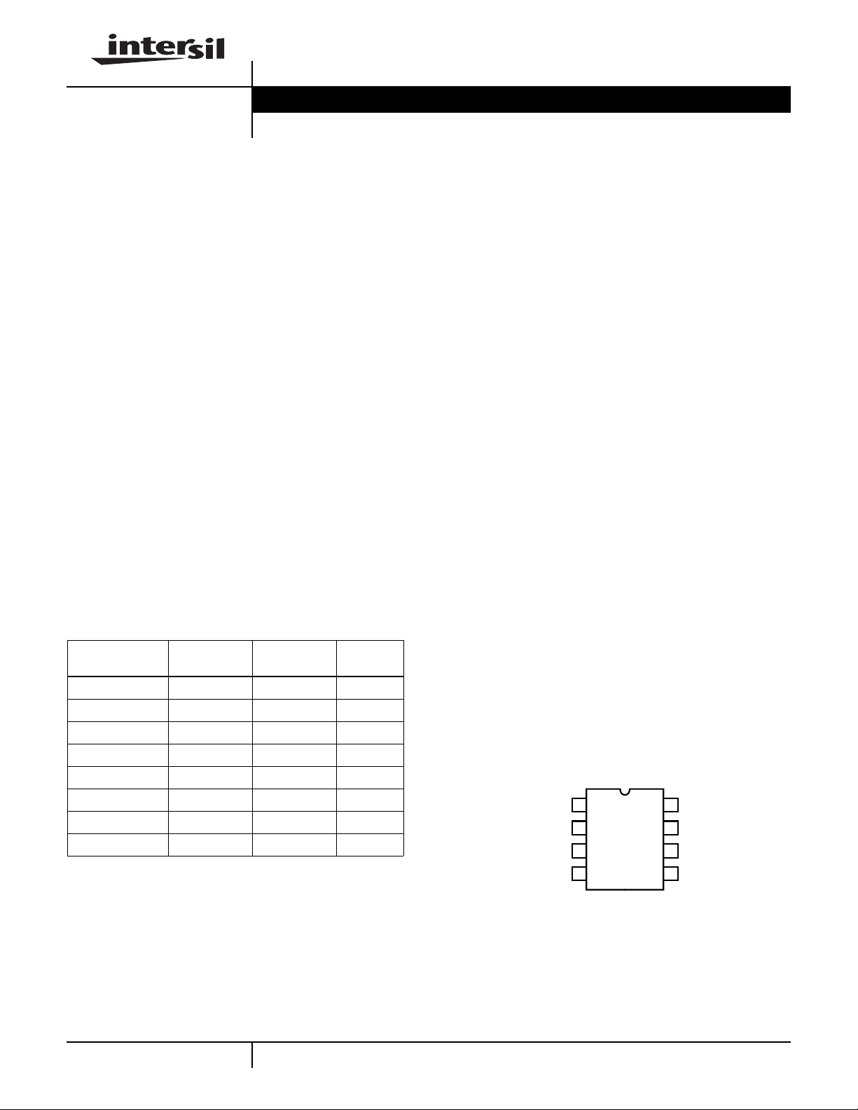
Ordering Information
TEMP. RANGE
PART NUMBER
ICL7663SCBA 0 to 70 8 Ld SOIC (N) M8.15
ICL7663SCPA 0 to 70 8 Ld PDIP E8.3
ICL7663SACBA 0 to 70 8 Ld SOIC (N) M8.15
ICL7663SACPA 0 to 70 8 Ld PDIP E8.3
ICL7663SIBA -25 to 85 8 Ld SOIC (N) M8.15
ICL7663SIPA -25 to 85 8 Ld PDIP E8.3
ICL7663SAIBA -25 to 85 8 Ld SOIC (N) M8.15
ICL7663SAIPA -25 to 85 8 Ld PDIP E8.3
(oC) PACKAGE PKG. NO.
• Handheld Instruments
• LCD Display Modules
• Remote Data Loggers
• Battery-Powered Systems
Pinout
ICL7663S
(PDIP, CERDIP, SOIC)
TOP VIEW
V
OUT2
V
OUT1
GND
1
2
3
4
SENSE
8
7
6
5
VIN+
V
TC
V
SET
SHDN
3-55
CAUTION: These devices are sensitive to electrostatic discharge; follow proper IC Handling Procedures.
http://www.intersil.com or 407-727-9207
| Copyright © Intersil Corporation 1999
Page 2
ICL7663S
Absolute Maximum Ratings Thermal Information
Input Supply Voltage . . . . . . . . . . . . . . . . . . . . . . . . . . . . . . . . +18V
Any Input or Output Voltage (Note 1)
Terminals 1, 2, 3, 5, 6, 7. . . . . . . . . . . . . VIN+ 0.3V to GND -0.3V
Output Source Current
Terminal 2. . . . . . . . . . . . . . . . . . . . . . . . . . . . . . . . . . . . . . . 50mA
Terminal 3. . . . . . . . . . . . . . . . . . . . . . . . . . . . . . . . . . . . . . . 25mA
Output Sinking Current
Terminal 7. . . . . . . . . . . . . . . . . . . . . . . . . . . . . . . . . . . . . . -10mA
Operating Conditions
Temperature Range
ICL7663SC. . . . . . . . . . . . . . . . . . . . . . . . . . . . . . . . . 0oC to 70oC
ICL7663SI . . . . . . . . . . . . . . . . . . . . . . . . . . . . . . . -25oC to 85oC
CAUTION: Stresses above those listed in “Absolute Maximum Ratings” may cause permanent damage to the device. This is a stress only rating and operationofthe
device at these or any other conditions above those indicated in the operational sections of this specification is not implied.
NOTES:
1. Connecting any terminal to voltages greater than (V+IN + 0.3V) or less than (GND - 0.3V) may cause destructive device latch-up. It is recommended that no inputs from sources operating on external power supplies be applied prior to ICL7663S power-up.
2. θJA is measured with the component mounted on an evaluation PC board in free air.
Thermal Resistance (Typical, Note 2) θJA (oC/W) θJC (oC/W)
CERDIP Package. . . . . . . . . . . . . . . . . 115 30
PDIP Package . . . . . . . . . . . . . . . . . . . 150 N/A
Plastic SOIC Package . . . . . . . . . . . . . 180 N/A
Maximum Junction Temperature
PDIP Package . . . . . . . . . . . . . . . . . . . . . . . . . . . . . . . . . 150oC
CERDIP Package. . . . . . . . . . . . . . . . . . . . . . . . . . . . . . . 175oC
Maximum Storage Temperature Range. . . . . . . . . . -65oC to 150oC
Maximum Lead Temperature (Soldering 10s) . . . . . . . . . . . . .300oC
(SOIC - Lead Tips Only)
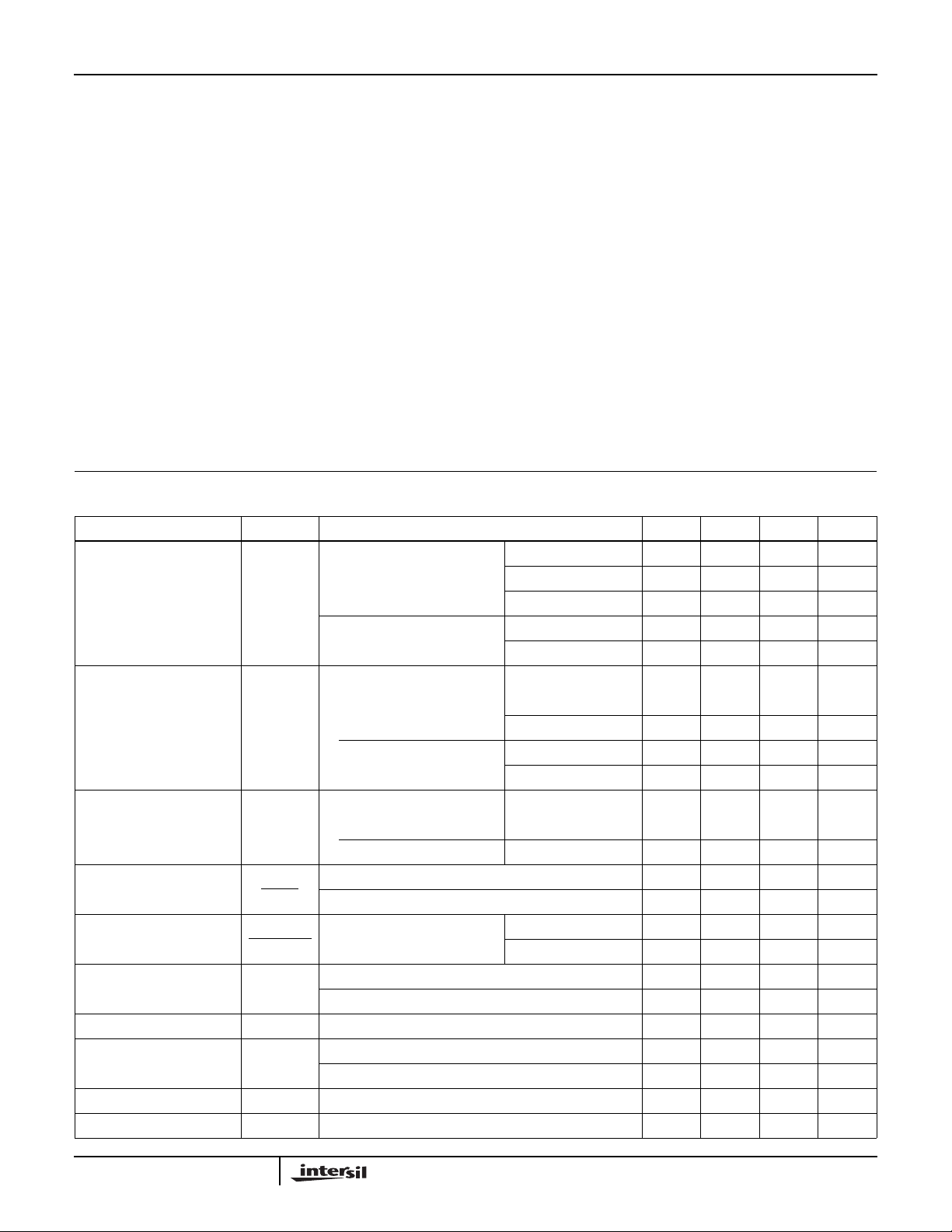
Electrical Specifications Specifications Below Applicable to Both ICL7663S and ICL7663SA, Unless Otherwise Specified. V+
V
= 5V, TA = 25oC, Unless Otherwise Specified. Notes 4, 5. See Test Circuit, Figure 7
OUT
PARAMETER SYMBOL TEST CONDITIONS MIN TYP MAX UNITS
Input Voltage V+
Quiescent Current I
Reference Voltage V
Temperature
∆V
Coefficient
Line Regulation ∆V
V
SET’∆VIN
V
Input Current I
SET
Shutdown Input Current I
Shutdown Input Voltage V
Sense Pin Input Current I
SHDN
SHDN
SENSE
Sense Pin Input Threshold V
SET
∆T
SET
ICL7663S TA = 25oC 1.5 - 16 V
IN
0oC < TA < 70oC 1.6 - 16 V
-25oC < TA < 85oC 1.6 - 16 V
ICL7663SA 0oC < TA < 70oC 1.6 - 16 V
-25oC < TA < 85oC 1.6 - 16 V
1.4V ≤ V
Q
≤ 8.5V, No Load
OUT
V+IN = 9V 0oC < TA < 70oC--10µA
-25oC < TA < 85oC--10µA
V+IN = 16V 0oC < TA < 70oC--12µA
-25oC < TA < 85oC--12µA
I
OUT1
= 100µA, V
OUT
= V
SET
ICL7663S TA = 25oC 1.2 1.3 1.4 V
ICL7663SA TA = 25oC 1.275 1.29 1.305 V
0oC < TA < 70oC - 100 - ppm
SET
-25oC < TA < 85oC - 100 - ppm
2V < VIN < 15V 0oC < TA < 70oC - 0.03 - %/V
SET
-25oC < TA < 85oC - 0.03 0.3 %/V
0oC < TA < 70oC - 0.01 10 nA
-25oC < TA < 85oC - 0.01 10 nA
- ±0.01 10 nA
V
SHDN
V
SHDN
HI: Both V
LO: Both V
Disabled 1.4 - - V
OUT
Enable - - 0.3 V
OUT
- 0.01 10 nA
CL
- 0.5 - V
IN
= 9V,
3-56
Page 3
ICL7663S
Electrical Specifications Specifications Below Applicable to Both ICL7663S and ICL7663SA, Unless Otherwise Specified. V+
V
= 5V, TA = 25oC, Unless Otherwise Specified. Notes 4, 5. See Test Circuit, Figure 7 (Continued)
OUT
IN
= 9V,
PARAMETER SYMBOL TEST CONDITIONS MIN TYP MAX UNITS
Input-Output Saturation
Resistance (Note 3)
Load Regulation ∆V
Available Output Current
(V
)
OUT2
Negative Tempco Output
(Note 4)
Temperature Coefficient ∆V
R
SAT
OUT
∆I
OUT
I
OUT2
V
TC
I
TC
V+IN = 2V, I
V+IN = 9V, I
V+IN = 15V, I
1mA < I
OUT2
50µA < I
OUT1
3V ≤ VIN≤ 16V, VIN - V
= 1mA - 170 350 Ω
OUT1
= 2mA - 50 100 Ω
OUT1
= 5mA - 35 70 Ω
OUT1
< 20mA - 1 3 Ω
< 5mA - 2 10 Ω
= 1.5V 40 - - mA
OUT2
Open Circuit Voltage - 0.9 - V
Maximum Sink Current 0 8 2.0 mA
Open Circuit - +2.5 - mV/oC
TC
∆T
Minimum Load Current I
L(MIN)
Includes V
Divider TA = 25oC - - 1.0 µA
SET
0oC < TA < 70oC - 0.2 5.0 µA
-25oC < TA < 85oC - 0.2 5.0 µA
NOTES:
3. Thisparameter referstothe saturation resistance of the MOS passtransistor.The minimum input-output voltage differential at lowcurrent(under
5mA), can be determined by multiplying the load current (including set resistor current, but not quiescent current) by this resistance.
4. This output has a positive temperature coefficient. Using it in combination with the inverting input of the regulator at V
, a negative
SET
coefficient results in the output voltage. See Figure 9 for details. Pin will not source current.
5. All pins are designed to withstand electrostatic discharge (ESD) levels in excess of 2000V.
6. All significant improvements over the industry standard ICL7663 are highlighted.
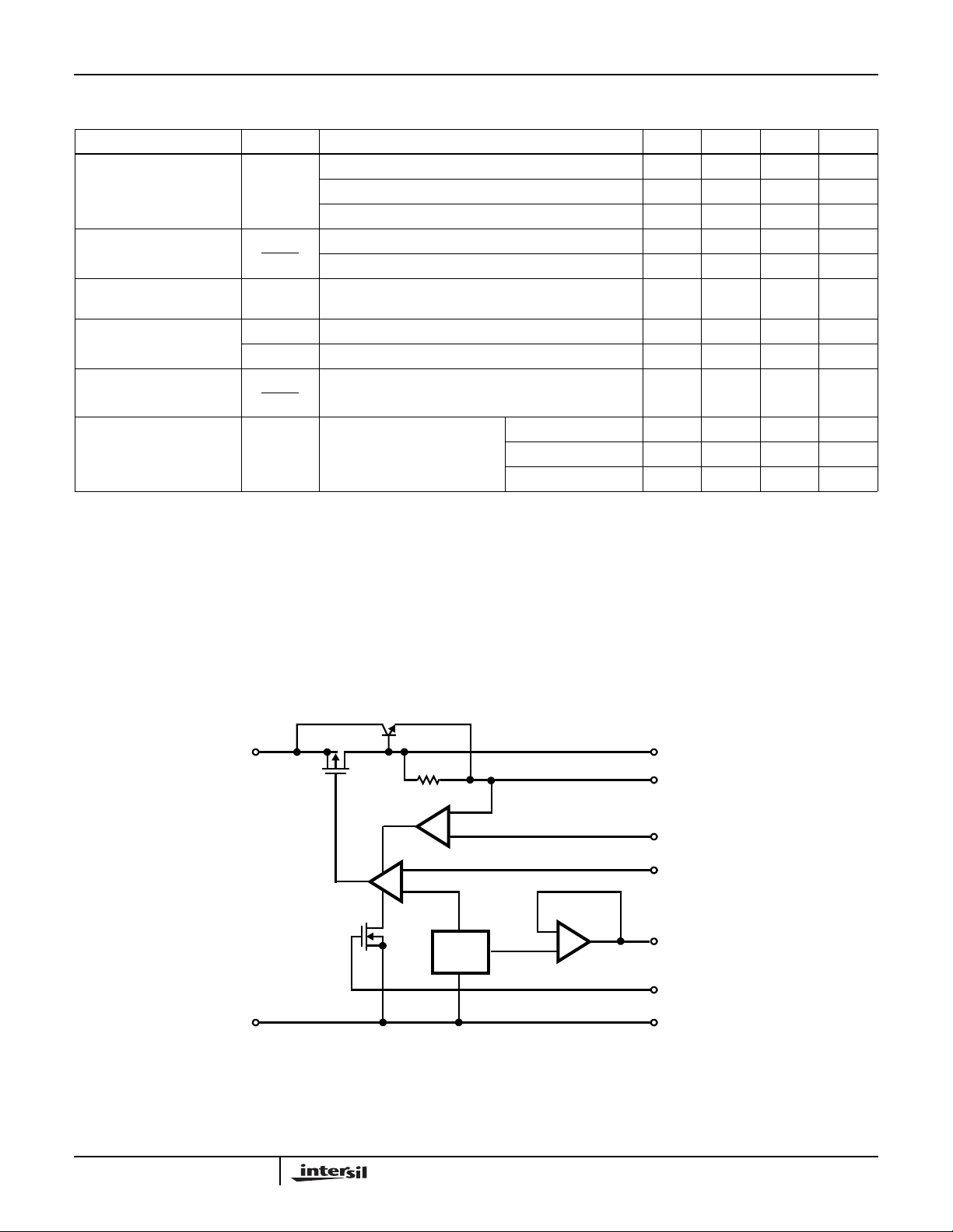
Functional Diagram
V+
GND
8
IN
C
A
REF
B
3
V
2
V
1
SENSE
6
V
7
V
5
SHUTDOWN
4
GND
OUT1
OUT2
SET
TC
3-57
Page 4

Typical Performance Curves
5.000
(V)
OUT
V
4.995
4.990
4.985
4.980
4.975
4.970
4.965
4.960
4.955
4.950
-3
10
-2
10
TA = 25oC
V+ = 9.0V
-1
10
I
(mA)
OUT
10
ICL7663S
2.0
1.8
1.6
1.4
1.2
1 (V)
1.0
OUT
- V
0.8
IN
V+
0.6
0.4
0.2
0
1
10
2
10
0
02468101214161820
V+IN = 2V
V+IN = 9V
I
OUT1
TA = 25oC
V+IN = 15V
(mA)
FIGURE 1. V
OUTPUT VOLTAGE AS A FUNCTION OF
OUT2
OUTPUT CURRENT
2.0
1.8
TA = 25oC
1.6
1.4
1.2
1 (V)
1.0
OUT
- V
0.8
IN
V+
0.6
0.4
0.2
0
0 5 10 15 20 25 30 35 40 45 50
I
(mA)
OUT2
FIGURE 3. V
INPUT-OUTPUT DIFFERENTIAL vs
OUT2
V+IN = 2V
V+IN = 9V
V+IN = 15V
OUTPUT CURRENT
5.0
4.5
4.0
3.5
3.0
2.5
(µA)
O
I
2.0
1.5
1.0
0.5
0
0246810121416
TA = -20oC
TA = -25oC
TA = -70oC
V+
(V)
IN
FIGURE 2. V
INPUT-OUTPUT DIFFERENTIAL vs
OUT1
OUTPUT CURRENT
100
90
80
70
60
50
PSRR (dB)
40
30
20
10
0
-2
10
-1
10
VIN = 9.0V
∆V
= 2V
IN
0
10
FREQUENCY (Hz)
1
10
2
10
FIGURE 4. NPUT POWER SUPPLY REJECTION RATIO
5.00
4.75
4.50
4.25
4.00
3.75
(µA)
O
I
3.50
3.25
3.00
2.75
2.50
-20 0 20 40 60 80
V+ = 15V
V+ = 2V
TEMPERATURE (
V+ = 9V
o
C)
1k
FIGURE 5. QUIESCENT CURRENT AS A FUNCTION OF
INPUT VOLTAGE
3-58
FIGURE 6. QUIESCENT CURRENT AS A FUNCTION OF
TEMPERATURE
Page 5

ICL7663S
Detailed Description
The ICL7663S is a CMOS integrated circuit incorporating all
the functions of a voltage regulator plus protection circuitry
on a single monolithic chip. Referring to the Functional
Diagram, the main blocks are a bandgap-type voltage
reference, an error amplifier, and an output driver with both
PMOS and NPN pass transistors.
The bandgap output voltage, trimmed to 1.29V ±15mV for
the ICL7663SA, and the input voltage at the V
SET
terminal
are compared in amplifier A. Error amplifier A drives a
P-channel pass transistor which is sufficient for low (under
about 5mA) currents. The high current output is passed by
an NPN bipolar transistor connected as a follower. This
configuration gives more gain and lower output impedance.
Logic-controlled shutdown is implemented via a N-Channel
MOS transistor. Current-sensing is achieved with
comparator C, which functions with the V
ICL7663S has an output (V
) from a buffer amplifier (B),
TC
OUT2
terminal. The
which can be used in combination with amplifier A to
generate programmable-temperature-coefficient output
voltages.
The amplifier, reference and comparator circuitry all operate
at bias levels well below 1µA to achieve extremely low
quiescent current. This does limit the dynamic response of
the circuits, however, and transients are best dealt with
outside the regulator loop.
Basic Operation
The ICL7663S is designed to regulate battery voltages in the
5V to 15V region at maximum load currents of about 5mA to
30mA. Although intended as low power devices, power
dissipation limits must be observed. For example, the power
dissipation in the case of a 10V supply regulated down to 2V
with a load current of 30mA clearly exceeds the power
dissipation rating of the Mini-DIP:
(10 - 2) (30) (10
The circuit of Figure 8 illustrates proper use of the device.
CMOS devices generally require two precautions: every
input pin must go somewhere, and maximum values of
applied voltages and current limits must be rigorously
observed. Neglecting these precautions may lead to, at the
least, incorrect or nonoperation, and at worst, destructive
device failure. To avoid the problem of latchup, do not apply
inputs to any pins before supply voltage is applied.
Input Voltages - The ICL7663S accepts working inputs of
1.5V to 16V. When power is applied, the rate-of-rise of the
input may be hundreds of volts per microsecond. This is
potentially harmful to the regulators, where internal
operating currents are in the nanoampere range. The
0.047µF capacitor on the device side of the switch will limit
inputs to a safe level around 2V/µs. Use of this capacitor is
suggested in all applications. In severe rate-of-rise cases, it
-3
) = 240mW
may be advisable to use an RC network on the SHutDowN
pin to delay output turn-on. Battery charging surges,
transients, and assorted noise signals should be kept from
the regulators by RC filtering, zener protection, or even
fusing.
SENSE
V
OUT2
V
OUT1
V
GND
+
M
I
Q
OUT1
and V
TC
V
SET
SHDN
S
, open S2 for V
.
OUT2
0.047µF
+
-
NOTES:
7. S1when closed disables output current limiting.
8. Close S2 for V
9. IQ quiescent currents measured at GND pin by meter M.
10. S3when ON, permits normal operation, when OFF, shuts down
both V
OUT1
FIGURE 7. ICL7663S TEST CIRCUIT
Output Voltages - The resistor divider R
scale the reference voltage, V
using the formula V
= (1 + R2/R1) V
OUT
R
CL
S
S
3
1
2
(7663 ONLY)
ON
OFF
1MΩ
, to the desired output
SET
OUT2
1.4V < V
.
2/R1
SET
V
OUT
R
2
R
L
R
1
1µA MIN
SHDN
is used to
. Suitable
< V+
C
L
arrangements of these resistors, using a potentiometer,
enables exact values for V
to be obtained. In most
OUT
applications the potentiometer may be eliminated by using
the ICL7663SA. The ICL7663SA has V
SET
voltage
guaranteed to be 1.29V ±15mV and when used with ±1%
tolerance resistors for R
and R2 the initial output voltage
1
will be within ±2.7% of ideal.
The low leakage current of the V
R
to be tens of megohms forminimum additional quiescent
2
terminal allows R1and
SET
drain current. However, some load current is required for
proper operation, so for extremely low-drain applications it is
necessary to draw at least 1µA. This can include the current
for R
and R1.
2
Output voltages up to nearly the VINsupply may be obtained
at low load currents, while the low limit is the reference
voltage. The minimum input-output differential in each
regulator is obtained using the V
output differential increases to 1.5V when using V
, terminal. The input-
OUT1
OUT2
.
Output Currents - Low output currents of less than 5mA are
obtained with the least input-output differential from the
V
terminal (connect V
OUT1
currents are needed, use V
OUT2
OUT2
to V
(V
). Where higher
OUT1
, should be left
OUT1
open in this case).
IN
3-59
Page 6

W
V
T
ICL7663S
High output currents can be obtained only as far as package
dissipation allows. It is strongly recommended that output
current-limit sensing be used in such cases.
Current-Limit Sensing - The on-chip comparator (C in the
Functional Diagram) permits shutdown of the regulator
output in the event of excessive current drain. As Figure 8
shows, a current-limiting resistor, R
with V
load side of R
and the SENSE terminal is connected to the
OUT2
. When the current through RCL is high
CL
enough to produce a voltage drop equal to V
, is placed in series
CL
(0.5V) the
CL
voltage feedback is by-passed and the regulator output will
be limited to this current. Therefore,when the maximum load
current (I
obtain the value for R
V
IN
V
=
OUT
ICL =
FIGURE 8. POSITIVE REGULATOR WITH CURRENT LIMIT
) is determined, simply divide VCLby I
LOAD
R
2
V
R
+ R
R
1
CL
CL
0.047µF
1
= 25mA
V
SET
CL
V+
GND
.
IN
= 5V
SENSE
V
OUT2
V
OUT1
V
V
SET
SHDN
TC
20Ω
R
CL
604kΩ
210kΩ
LOAD
R
2
10µF
V
OUT
C
L
+5V
R
1
the regulated output voltage reaches 90% of its final value in
20ms. From:
I =∆VC,C
∆t
I
OUT
=
(20 x 10-3)
0.9V
OUT
= 0.022
I
OUT
V
OUT
In addition, where such a capacitor is used, a current-limiting
resistor is also suggested (see “Current-Limit Sensing”).
Producing Output Voltages with Negative Temperature
Coefficients -The ICL7663S has an additional output which
is 0.9V relative to GND and has a tempco of +2.5mV/
o
C. By
applying this voltage to the inverting input of amplifier A (i.e.,
the V
to
produced. The TC of the output voltage is controlled by the
R
2/R3
EQ. 1: V
EQ. 2: TC V
TC
pin), output voltages having negative TC may be
SET
ratio (see Figure 9 and its design equations).
here:V
OUT
SET
+
V
TC
-
= V
SET
OUT
= 1.3V
R
1
R
3
=
V
SET
( R
1 +
-
R
2
+
+
V
REF
-
) R
2
+
R
R
1
R
2
(TC VTC) in mV/oC
R
3
2
(V
- VTC)
SET
3
= 0.9V
V
OUT
CVTC = +2.5mV/oC
FIGURE 9. GENERATING NEGATIVE TEMPERATURE
COEFFICIENTS
Logic-Controllable Shutdown - When equipment is not
needed continuously (e.g., in remote data-acquisition
systems), it is desirable to eliminate its drain on the system
until it is required. This usually means switches, with their
unreliable contacts. Instead, the ICL7663S can be shut
down by a logic signal, leaving only I
(under 4µA) as a
Q
drain on the power source. Since this pin must not be left
open, it should be tied to ground if not needed. A voltage of
less than 0.3V for the ICL7663S will keep the regulator ON,
and a voltage level of more than 1.4V but less than V+
IN
will
turn the outputs OFF. If there is a possibility that the control
signal could exceed the regulator input (V+
) the current
IN
from this signal should be limited to 100µA maximum by a
high value (1MΩ) series resistor. This situation may occur
when the logic signal originates from a system powered
separately from that of the regulator.
Additional Circuit Precautions - This regulator has poor
rejection of voltage fluctuations from AC sources above
10Hz or so. To prevent the output from responding (where
this might be a problem), a reservoir capacitor across the
load is advised. The value of this capacitor is chosen so that
3-60
Applications
Boosting Output Current with External Transistor
The maximum availableoutput current from the ICL7663S is
40mA. To obtain output currents greater than 40mA, an
external NPN transistor is used connected as shown in
Figure 10.
V
V+
OUT1
IN
V
IN
10µF
SENSE
GND
V
OUT2
V
SET
SHDN
100Ω
FIGURE 10. BOOSTINGOUTPUT CURRENT WITH EXTERNAL
TRANSISTOR
EXTERNAL PIN
POWER
TRANSISTOR
0.47Ω
604kΩ
210kΩ
V
OUT
+5V
Page 7

ICL7663S
Generating a Temperature Compensated Display Drive Voltage
Temperature has an important effect in the variation of
threshold voltage in multiplexed LCD displays. As
temperature rises, the threshold voltage goes down. For
applications where the display temperature varies widely, a
+5V
LOGIC
SYSTEM,
PROCESSOR,
ETC.
ICL7663S
V+
IN
V
OUT1
V
OUT2
V
temperature compensated display voltage, V
generated using the ICL7663S. This is shown in Figure 11
for the ICM7233 triplexed LCD display driver.
1.8MΩ
SET
300kΩ
V
TC
V+
ICM7233
DISP
, can be
GND
DATA BUS
2.7MΩ
V
DISP
GND
GND
FIGURE 11. GENERATING A MULTIPLEXED LCD DISPLAY DRIVE VOLTAGE
All Intersil semiconductor products are manufactured, assembled and tested under ISO9000 quality systems certification.
Intersil semiconductor products are sold by description only. Intersil Corporation reserves the right to make changes in circuit design and/or specifications at any time without notice. Accordingly, the reader is cautioned to verify that data sheets are current before placing orders. Information furnished by Intersil is believed to be accurate and
reliable. However,no responsibility is assumed by Intersil or its subsidiaries for its use; nor for any infringements of patents or other rights of third parties which may result
from its use. No license is granted by implication or otherwise under any patent or patent rights of Intersil or its subsidiaries.
For information regarding Intersil Corporation and its products, see web site http://www.intersil.com
Sales Office Headquarters
NORTH AMERICA
Intersil Corporation
P. O. Box 883, Mail Stop 53-204
Melbourne, FL 32902
TEL: (407) 724-7000
FAX: (407) 724-7240
3-61
EUROPE
Intersil SA
Mercure Center
100, Rue de la Fusee
1130 Brussels, Belgium
TEL: (32) 2.724.2111
FAX: (32) 2.724.22.05
ASIA
Intersil (Taiwan) Ltd.
7F-6, No. 101 Fu Hsing North Road
Taipei, Taiwan
Republic of China
TEL: (886) 2 2716 9310
FAX: (886) 2 2715 3029
 Loading...