

Datasheet ICL7650BCD, ICL7650BCPA, ICL7650BCPD, ICL7650BCSA, ICL7650BCSD Datasheet (Maxim Integrated Producs)
...
General Description
Maxim’s ICL7650/ICL7653 are chopper-stabilized
amplifiers, ideal for low-level signal processing applications. Featuring high performance and versatility, these
devices combine low input offset voltage, low input bias
current, wide bandwidth, and exceptionally low drift
over time and temperature. Low offset is achieved
through a nulling scheme that provides continuous
error correction. A nulling amplifier alternately nulls
itself and the main amplifier. The result is an input offset
voltage that is held to a minimum over the entire operating temperature range.
The ICL7650B/ICL7653B are exact replacements for
Intersil’s ICL7650B/ICL7653B. These devices have a
10µV max offset voltage, a 0.1µV/°C max input offset
voltage temperature coefficient, and a 20pA max bias
current—all specified over the commercial temperature
range.
A 14-pin version is available that can be used with
either an internal or external clock. The 14-pin version
has an output voltage clamp circuit to minimize overload recovery time.
Applications
Condition Amplifier
Precision Amplifier
Instrumentation Amplifier
Thermocouples
Thermistors
Strain Gauges
Features
♦ ICL7650/53 are Improved Second Sources to
ICL7650B/53B
♦ Lower Supply Current: 2mA
♦ Low Offset Voltage: 1µV
♦ No Offset Voltage Trimming Needed
♦ High-Gain CMRR and PSRR: 120dB min
♦ Lower Offset Drift with Time and Temperature
♦ Extended Common-Mode Voltage Range
♦ Low DC Input Bias Current: 10pA
♦ Monolithic, Low-Power CMOS Design
ICL7650/ICL7650B/ICL7653/ICL7653B
Chopper-Stabilized Op Amps
________________________________________________________________ Maxim Integrated Products 1
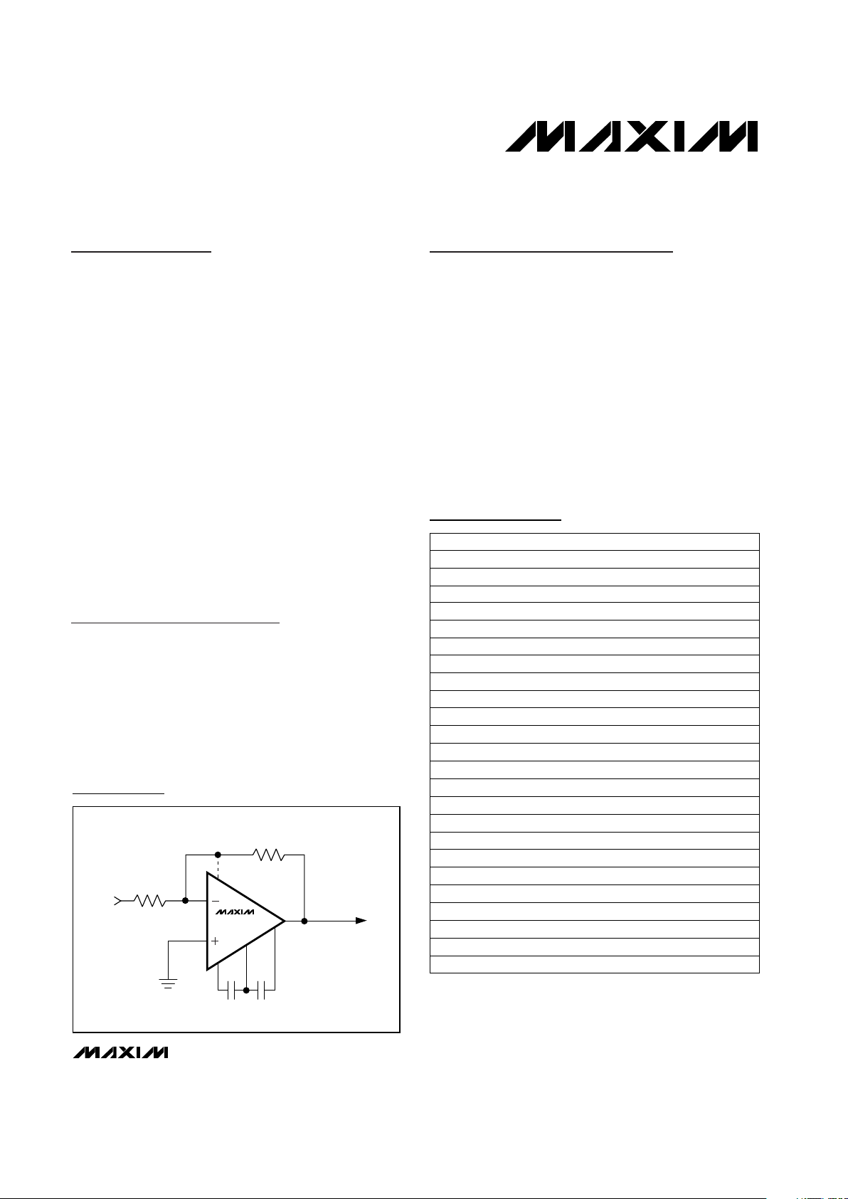
ICL7650
ICL7653
OUTPUT
INVERTING AMPLIFIER
WITH OPTIONAL CLAMP
INPUT
C
R
C
CLAMP
Typical Operating Circuit
19-0960; Rev 2; 1/00
Pin Configurations appear at end of data sheet.
Ordering Information
PART
ICL7650CSA
ICL7650CSD
ICL7650CPA 0°C to +70°C
0°C to +70°C
0°C to +70°C
TEMP. RANGE PIN-PACKAGE
8 SO
14 SO
8 Plastic DIP
ICL7650CPD
ICL7650CTV
ICL7650C/D 0°C to +70°C
0°C to +70°C
0°C to +70°C 14 Plastic DIP
8 TO-99
Dice
ICL7650IJA
ICL7650IJD -20°C to +85°C
-20°C to +85°C 8 CERDIP
14 CERDIP
ICL7650MTV
ICL7650MJD -55°C to +125°C
-55°C to +125°C 8 CERDIP
14 CERDIP
ICL7650BCSA
ICL7650BCSD 0°C to +70°C
0°C to +70°C 8 SO
14 SO
ICL7650BCPA
ICL7650BCPD 0°C to +70°C
0°C to +70°C 8 Plastic DIP
14 Plastic DIP
ICL7650BCTV
ICL7650BC/D 0°C to +70°C
0°C to +70°C 8 TO-99
Dice
ICL7653CSA
ICL7653CPA
ICL7653CTV
0°C to +70°C 8 SO
ICL7653BCSA
ICL7653BCPA
0°C to +70°C
0°C to +70°C 8 Plastic DIP
8 TO-99
0°C to +70°C
ICL7653IJA
ICL7653MTV -55°C to +125°C
-20°C to +85°C 8 CERDIP
8 CERDIP
0°C to +70°C 8 SO
8 Plastic DIP
ICL7653BCTV 0°C to +70°C 8 TO-99
For free samples and the latest literature, visit www.maxim-ic.com or phone 1-800-998-8800.
For small orders, phone 1-800-835-8769.
ICL7650/ICL7650B/ICL7653/ICL7653B
Chopper-Stabilized Op Amps
2 _______________________________________________________________________________________
ABSOLUTE MAXIMUM RATINGS
ELECTRICAL CHARACTERISTICS—ICL7650B/ICL7653B
(Circuit of Figure 1, V+ = +5V, V- = -5V, TA= +25°C, unless otherwise noted.)
Stresses beyond those listed under “Absolute Maximum Ratings” may cause permanent damage to the device. These are stress ratings only, and functional
operation of the device at these or any other conditions beyond those indicated in the operational sections of the specifications is not implied. Exposure to
absolute maximum rating conditions for extended periods may affect device reliability.
Total Supply Voltage (V+ to V-)..............................................18V
Input Voltage ........................................(V+ + 0.3V) to (V- - 0.3V)
Voltage on Oscillator Control Pins
(except EXT/CLOCK IN).............................................V+ to V-
Voltage on EXT/CLOCK IN ..................(V+ + 0.3V) to (V+ - 6.0V)
Duration of Output Short Circuit ....................................Indefinite
Current into Any Pin ............................................................10mA
Current into Any Pin while Operating (Note 1)...................100µA
Continuous Total Power Dissipation (T
A
= +70°C)
8-Pin SO (derate 5.88mW/°C above +70°C)...............471mW
8-Pin PDIP (derate 6.9mW/°C above +70°C)...............552mW
8-Pin CERDIP (derate 8.0mW/°C above +70°C).........640mW
8-Pin TO-99 (derate 6.7mW/°C above +70°C)............533mW
14-Pin SO (derate 8.3mW/°C above +70°C)...............667mW
14-Pin PDIP (derate 10.0mW/°C above +70°C)..........800mW
14-Pin CERDIP (derate 9.1mW/°C above +70°C).......727mW
Operating Temperature Ranges
ICL765_C_ _/ICL755_BC_ _ ...............................0°C to +70°C
ICL765_I__/ICL755_BI__ ................................-20°C to +85°C
ICL765_M__/ICL755_BM__ ..........................-55°C to +125°C
Storage Temperature Range .............................-65°C to +150°C
Junction Temperature......................................................+150°C
Lead Temperature (soldering, 10s) .................................+300°C
CL= 50pF, RL= 10kΩ
f = 10Hz
RS= 100Ω, f = 0 to 10Hz
V+ to V- = ±3V to ±8V
CMVR = -5V to +1.6V
RL= 100kΩ
RL= 10kΩ
RL= 10kΩ
Doubles every 10°
-20°C < TA< +85°C
TA= +25°C
-55°C < TA< +85°C
-55°C < TA< +125°C
TA= +25°C
TA= +25°C
CONDITIONS
µs0.2t
r
Rise Time
V/µs2.5SRSlew Rate
MHz2.0GBWUnity-Gain Bandwidth
pA/√Hz
0.01I
n
Input Noise Current
µVp-p2e
np-p
Input Noise Voltage
dB120 130PSRRPower-Supply Rejection Ratio
dB120 130CMRRCommon-Mode Rejection Ratio
V-5.0 -5.2 to +2.0 1.6CMVRCommon-Mode Voltage Range
±4.95
V
±4.7 ±4.85
V
OUT
Output Voltage Swing (Note 3)
V/V
1 · 1055 · 10
8
A
VOL
Large-Signal Voltage Gain
Ω
10
12
R
IN
Input Resistance
pA0.5I
OS
Input Offset Current (Note 2)
100
35
pA
1.5 10
I
BIAS
Input Bias Current
0.01 0.05
µV
±0.7 ±5
V
OS
Input Offset Voltage
±10
5.0
µV/°C
50
∆V
OS
∆T
Average Temperature Coefficient
of Input Offset Voltage
UNITSMIN TYP MAXSYMBOLPARAMETER
Note 1: Maxim recommends limiting the input current to 100µA to avoid latchup problems. A value of 1mA is typically safe; however,
this is not guaranteed.
TA= +25°C
0°C < TA< +70°C
-20°C < TA< +85°C
%20Overshoot
V4.5 16V+ to V-Operating Supply Range
No load mA2.0 3.5I
SUPP
Supply Current
ICL7650/ICL7650B/ICL7653/ICL7653B
Chopper-Stabilized Op Amps
_______________________________________________________________________________________ 3
ELECTRICAL CHARACTERISTICS—ICL7650/ICL7653
(Circuit of Figure 1, V+ = +5V, V- = -5V, TA= +25°C, unless otherwise noted.) (Note 5)
ELECTRICAL CHARACTERISTICS—ICL7650B/ICL7653B (continued)
(Circuit of Figure 1, V+ = +5V, V- = -5V, TA= +25°C, unless otherwise noted.)
Note 2: I
OS
= 2 · I
BIAS
Note 3: OUTPUT and CLAMP pins not connected.
Note 4: See Output Clamp section for details.
CONDITIONS UNITSMIN TYP MAXSYMBOLPARAMETER
-4.0V < V
OUT
< +4.0V pA1Clamp Off Current (Note 4)
No load
nV/
√month
100Offset Voltage vs. Time
0°C ≤ TA≤ +70°C
-20°C ≤ TA≤ +85°C
-55°C ≤ TA≤ +125°C
0°C ≤ TA≤ +70°C
RL= 100kΩ
RL= 10kΩ
-55°C ≤ TA≤ +125°C
ICL765_
TA= +25°C
ICL765_
(Note 6)
CONDITIONS
V
-5.0 -5.2 to +3.0 2.5
CMVRCommon-Mode Voltage Range
±4.95
V
±4.7 ±4.85
V
OUT
Output Voltage Swing (Note 3)
0.2 · 10
8
Ω
10
12
R
IN
Input Resistance
0.3 10
50 200
20 100
±10 ±50
µV
±0.7 ±5.0
V
OS
Input Offset Voltage
±1.0 ±10
±1.0 ±10
±1.0 ±10
UNITSMIN TYP MAXSYMBOLPARAMETER
ICL765_
ICL765_B, 0°C ≤ TA≤ +70°C
0.01 0.1
µV/°C
0.01 0.05
∆V
OS
∆T
Average Temperature Coefficient
of Input Offset Voltage (Note 6)
ICL765_
ICL765_B
0°C ≤ TA≤ +70°C
-20°C ≤ TA≤ +85°C
-55°C ≤ TA≤ +125°C
0.01 0.05
0.01 0.05
0.25 1.5
TA= +25°C
410
pAI
B
Input Bias Current
12 20ICL765_B
ICL765_
RL= 10kΩ, TA= +25°C
V/V
1 · 1085 · 10
8
A
VOL
Large-Signal Voltage Gain
0°C ≤ TA≤ +70°C
0.5 · 10
8
-20°C ≤ TA≤ +85°C
0.5 · 10
8
-20°C ≤ TA≤ +85°C -5.0 -5.2 to +3.0 2.5
-55°C ≤ TA≤ +125°C -4.5 -4.0 to +3.0 2.5
0°C ≤ TA≤ +70°C
-20°C ≤ TA≤ +85°C
-55°C ≤ TA≤ +85°C
+85°C ≤ TA≤ +125°C
RL= 100kΩ µA25 70 200Clamp On Current (Note 4)
Pins 12–14 open (DIP) Hz120 200 375f
ch
Internal Chopping Frequency
-30
-10
-20
1
0
3
2
4
2684 10121416
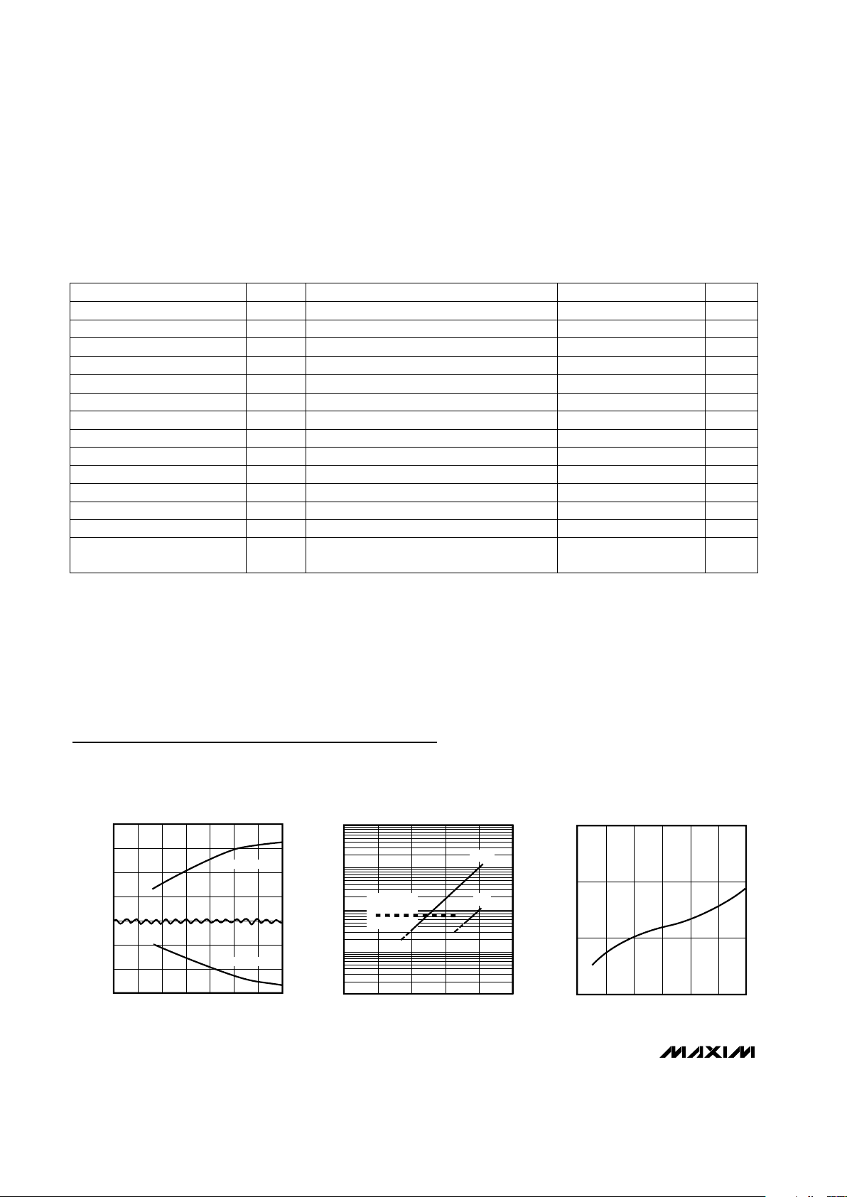
MAXIMUM OUTPUT CURRENT
vs. SUPPLY VOLTAGE
ICL7650toc01
TOTAL SUPPLY VOLTAGE (V)
MAXIMUM OUTPUT CURRENT (mA)
SOURCE CURRENT
SINK CURRENT
1k
100
10
1
0.1
25 7550 100 125 150
CLOCK RIPPLE REFERRED TO INPUT
vs. TEMPERATURE
ICL7650toc02
TEMPERATURE (°C)
CLOCK RIPPLE (µVp-p)
BROADBAND
NOISE
(A
V
= 1000)
0.1µF
1µF
0
1
2
3
48106 121416
SUPPLY CURRENT
vs. SUPPLY VOLTAGE
ICL7650toc03
TOTAL SUPPLY VOLTAGE (V)
SUPPLY CURRENT (mA)
Typical Operating Characteristics
(Circuit of Figure 1, V+ = +5V, V- = -5V, TA = +25°C, unless otherwise noted.)
ICL7650/ICL7650B/ICL7653/ICL7653B
Chopper-Stabilized Op Amps
4 _______________________________________________________________________________________
ELECTRICAL CHARACTERISTICS—ICL7650/ICL7653 (continued)
(Circuit of Figure 1, V+ = +5V, V- = -5V, TA= +25°C, unless otherwise noted.) (Note 5)
CL= 50pF, RL= 10kΩ
f = 10Hz
RS= 100Ω, f = 0 to 10Hz
V+ to V- = ±3V to ±8V
CMVR = -5V to +2.5V
%
CONDITIONS
µs0.2t
r
Rise Time
V/µs2.5SRSlew Rate
MHz2.0GBWUnity-Gain Bandwidth
pA/√Hz
0.01I
n
Input Noise Current
µVp-p2e
np-p
Input Noise Voltage
dB120 130PSRRPower-Supply Rejection Ratio
dB120 130CMRRCommon-Mode Rejection Ratio
20Overshoot
V4.5 16V+ to V-Operating Supply Range
No load mA1.2 2.0I
SUPP
Supply Current
UNITSMIN TYP MAXSYMBOLPARAMETER
Pins 13 and 14 open (DIP) Hz120 200 375f
CLKOUT
Internal Chopping Frequency
RL= 100kΩ µA25 70 200Clamp On Current (Note 4)
-4.0 ≤ V
OUT
≤ +4.0V pA1Clamp Off Current (Note 4)
nV/
√month
100Offset Voltage vs. Time
Note 3: OUTPUT and CLAMP pins not connected.
Note 4: See Output Clamp section for details.
Note 5: All pins are designed to withstand electrostatic discharge (ESD) levels in excess of 2000V (MIL STD 8838 Method 3015.1
test circuit).
Note 6: Sample tested. Limits are not used to calculate outgoing quality level.

ICL7650/ICL7650B/ICL7653/ICL7653B
Chopper-Stabilized Op Amps
_______________________________________________________________________________________ 5
0
1
2
3
-50 25 50-25 0 75 100 125
SUPPLY CURRENT vs.
AMBIENT TEMPERATURE
ICL7650toc04
AMBIENT TEMPERATURE (°C)
SUPPLY CURRENT (mA)
0
2
1
4
3
5
6
7
8
0231 45678
COMMON-MODE INPUT VOLTAGE RANGE
vs. SUPPLY VOLTAGE
ICL7650toc05
SUPPLY VOLTAGE (V)
COMMON-MODE INPUT VOLTAGE RANGE (V)
POSITIVE LIMIT
NEGATIVE LIMIT
0
-2
-6
-4
-8
-10
10 100 1k 10k
INPUT OFFSET VOLTAGE
vs. CHOPPING FREQUENCY
ICL7650toc06
CHOPPING FREQUENCY (CLOCK OUT) (Hz)
OFFSET VOLTAGE (µV)
3
1
2
-1
0
-2
-3
48106 121416
INPUT OFFSET VOLTAGE CHANGE
vs. SUPPLY VOLTAGE
ICL7650toc07
TOTAL SUPPLY VOLTAGE (V)
INPUT OFFSET VOLTAGE CHANGE (µV)
0
1
3
2
4
5
10 100 1k 10k
10Hzp-p NOISE VOLTAGE
vs. CHOPPING FREQUENCY
ICL7650toc08
CHOPPING FREQUENCY (CLOCK-OUT) (Hz)
DC TO 10Hz P-P NOISE VOLTAGE (µV)
20
60
40
100
80
140
120
160
0.01 1 100.1 100 1k 10k 100k
OPEN-LOOP GAIN AND PHASE SHIFT
vs. FREQUENCY
ICL7650toac09
FREQUENCY (Hz)
OPEN-LOOP GAIN (dB)
110
130
70
90
50
PHASE SHIFT (DEGREES)
RL = 10kΩ
C
EXT
= 0.1µF
20
60
40
100
80
140
120
160
0.01 1 100.1 100 1k 10k 100k
OPEN-LOOP GAIN AND PHASE SHIFT
vs. FREQUENCY
ICL7650toac10
FREQUENCY (Hz)
OPEN-LOOP GAIN (dB)
110
130
70
90
50
PHASE SHIFT (DEGREES)
RL = 10kΩ
C
EXT
= 1.0µF
-3
-2
-1
0
1
2
3
-1.0 0-0.5 0.5 1.0 1.5 2.0 2.5 3.0
VOLTAGE FOLLOWER LARGE-SIGNAL
PULSE RESPONSE
ICL7650toc11
TIME (µs)
OUTPUT VOLTAGE (V)
CLOCK OUT HIGH
CLOCK OUT LOW
-3
-2
-1
0
1
2
3
-1.0 0-0.5 0.5 1.0 1.5 2.0 2.5 3.0
VOLTAGE FOLLOWER LARGE-SIGNAL
PULSE RESPONSE
ICL7650toc12
TIME (µs)
OUTPUT VOLTAGE (V)
CLOCK OUT HIGH
CLOCK OUT LOW
Typical Operating Characteristics (continued)
(Circuit of Figure 1, V+ = +5V, V- = -5V, TA = +25°C, unless otherwise noted.)

ICL7650/ICL7650B/ICL7653/ICL7653B
Chopper-Stabilized Op Amps
6 _______________________________________________________________________________________
Detailed Description
Figure 2 shows the major elements of the ICL7650/
ICL7653. Two amplifiers are illustrated, the main amplifier and the nulling amplifier, both of which have offsetnull capability. The main amplifier is connected full time
from the input to the output. The nulling amplifier, under
control of the chopper-frequency oscillator and clock
circuit, alternately nulls itself and the main amplifier. This
nulling arrangement, which is independent of the output
level, operates over the full power-supply and commonmode ranges. The ICL7650/ICL7653 exhibit an exceptionally high CMRR, PSRR, and A
VOL
. Their nulling
connections, which are MOSFET back gates, have inherently high impedance. Two external capacitors provide
storage for the nulling potentials and the necessary
nulling-loop time constants.
The ICL7650/ICL7653 minimize chopper-frequency
charge injection at the input terminals by carefully balancing the input switches. Feed-forward injection into
the compensation capacitor, the main cause of output
spikes in this type of circuit, is also minimized.
Output Clamp (ICL7650 Only)
The output clamp reduces the overload recovery time
inherent with chopper-stabilized amplifiers. When tied to
the summing junction or inverting input pin, a current path
between this point and the output occurs just before the
output device saturates. This prevents uncontrolled input
differential and the consequent charge build-up on the
correction-storage capacitors, while causing only a slight
reduction in the output swing.
Intermodulation
Intermodulation effects can cause problems in older
chopper-stabilized amplifier modules. Intermodulation
occurs since the amplifier has a finite AC gain, and
therefore will have a small AC signal at the input. In a
chopper-stabilized module, this small AC signal is
detected, chopped, and fed into the offset-correction
circuit. This results in spurious outputs at the sum and
difference frequencies of the chopping and input signal
frequencies. Other intermodulation effects in chopperstabilized modules include gain and phase anomalies
near the chopping frequency.
These effects are substantially reduced in the
ICL7650/ICL7653, which add to the nulling circuit a
dynamic current that compensates for the AC signal on
the inputs. Unlike modules, the ICL7650/ICL7653 can
precisely compensate for the finite AC gain, since both
the AC gain rolloff and the intermodulation compensation
current are controlled by internal matched capacitors.
ICL7650
ICL7653
OUTPUT
C
C
R
C
0.1µF 0.1µF
R2
1M
R1
1M
ICL7650
INTERNAL
BIAS
EXT CLK IN
CLK OUT
NULL
C
EXTA
C
EXTB
CAP RETURN
B
A
C
P
A
+
-
N
OUTPUT
+IN
-IN
CLAMP
MAIN
+
-
B
C
INT/EXT
A
A
A = CLK OUT
A
EXT CLK IN
B
C
OSC
Figure 1. ICL7650 Test Circuit
Figure 2. Block Diagram

ICL7650/ICL7650B/ICL7653/ICL7653B
Chopper-Stabilized Op Amps
_______________________________________________________________________________________ 7
Nulling Capacitor Connection
Separate pins are provided for C
RETN
and CLAMP in
the ICL7650. If you do not need the clamp feature,
order the ICL7653; this device only offers the C
RETN
pin
and will produce slightly lower noise and improved AC
common-mode rejection. If you need to use the clamp
feature, order the ICL7650 and connect the external
capacitors to V-. To prevent load-current IR drops and
other extraneous signals from being injected into the
capacitors, use a separate PC board trace to connect
the capacitor commons directly to the V- pin. The outside foil of the capacitors should be connected to the
low-impedance side of the null storage circuit, V- or
C
RETN
. This will act as an ESD voltage shield.
Clock Operation
The ICL7650’s internal oscillator generates a 200Hz frequency, which is available at the CLK OUT pin. The
device can also be operated with an external clock, if
desired. An internal pull-up permits the INT/EXT pin to
be left open for normal operation. However, the internal
clock must be disabled and INT/EXT must be tied to V-
if an external clock is used. An external clock signal
may then be applied to the EXT CLK IN pin. The duty
cycle of the external clock is not critical at low frequencies. However, a 50% to 80% positive duty cycle is preferred for frequencies above 500Hz, since the
capacitors are charged only when EXT CLK IN is high.
This ensures that any transients have time to settle
before the capacitors are turned off. The external clock
should swing between ground and V+ for power supplies up to ±6V, and between V+ and (V+ - 6V) for
higher supply voltages.
To avoid a capacitor imbalance during overload, use a
strobe signal. Neither capacitor will be charged if a
strobe signal is connected to EXT CLK IN so that it is
low while the overload signal is being applied to the
amplifier. A typical amplifier will drift less than 10µVs
since the leakage of the capacitor pins is quite low at
room temperature. Relatively long measurements may
be made with little change in offset.
Applications Information
Device Selection
In applications that require lowest noise, Maxim’s
ICL7652 may be preferred over the ICL7650/ICL7653.
The ICL7650/ICL7653 offer a higher gain-bandwidth
product and lower input bias currents, while the
ICL7652 reduces noise by using larger input FETs.
These larger FETs, however, increase the leakage at
the ICL7652’s external null pins. Therefore, the
ICL7650/ICL7653 can operate to a higher temperature
with 0.1µF capacitors before the clock ripple (due to
leakage at the null capacitor pins) becomes excessive
and 1µF external capacitors are required.
Output Stage/Load Driving
The ICL7650/ICL7653 somewhat resemble a transconductance amplifier whose open-loop gain is proportional
to load resistance. This behavior is apparent when loads
are less than the high-impedance stage (approximately
18kΩ for one output circuit). The open-loop gain, for
example, will be 17dB lower with a 1kΩ load than with a
10kΩ load. This lower gain is of little consequence if the
amplifier is used strictly for DC since the DC gain is typically greater than 120dB, even with a 1kΩ load. For
wideband applications, however, the best frequency
response will be achieved with a load resistor of 10kΩ or
higher. The result will be a smooth 6dB per octave
response from 0.1Hz to 2MHz, with phase shifts of less
than 10° in the transition region where the main amplifier
takes over from the null amplifier.
Component Selection
C
EXTA
and C
EXTB
, the two required capacitors, have
optimum values depending on the clock or chopping
frequency. The correct value is 0.1µF for the preset
internal clock. When using an external clock, scale this
component value in proportion to the relationship
between the chopping frequency and the nulling time
constant. A low-leakage ceramic capacitor may prove
suitable for many applications; however, a high-quality
film-type capacitor (such as mylar) is preferred. For
lowest settling time at initial turn-on, use capacitors with
low dielectric absorption (such as polypropylene
types). With low-dielectric-absorption capacitors, the
ICL7650/ICL7653 will settle to 1µV offset in 100ms, but
several seconds may be required if ceramic capacitors
are used.
Thermoelectric Effects
Thermoelectric effects developed in thermocouple
junctions of dissimilar materials (metals, alloys, silicon,
etc.) ultimately limit precision DC measurements.
Unless all junctions are at the same temperature, thermoelectric voltages (typically around 10µV/°C, but up
to hundreds of µV/°C for some materials) will be generated. In order to realize the extremely low offset voltages that the chopper amplifier can provide, take
special precautions to avoid temperature gradients. To
eliminate air movement, enclose all components (particularly those caused by power-dissipating elements in
the system). Minimize power-supply voltages and
power dissipation, and use low-thermoelectric-coefficient connections where possible. It is advisable to
separate the device surrounding heat-dissipating elements, and to use high-impedance loads.

ICL7650/ICL7650B/ICL7653/ICL7653B
Chopper-Stabilized Op Amps
8 _______________________________________________________________________________________
Input Guarding
Low-leakage, high-impedance CMOS inputs allow the
ICL7650/ICL7653 to measure high-impedance sources.
Stray leakage paths can decrease input resistance and
increase input currents unless inputs are guarded.
Boards must be thoroughly cleaned with TCE or alcohol
and blown dry with compressed air. The board should
be coated with epoxy or silicone after cleaning to prevent contamination.
Leakage currents may cause trouble even with properly
cleaned and coated boards, particularly since the input
pins are adjacent to pins that are at supply potentials.
Leakage can be significantly reduced by using guard-
ing to decrease the voltage difference between inputs
and adjacent metal runs. Use a 10-lead pin circle, with
the leads of the device formed so that the holes adjacent to the inputs are empty when it is inserted in the
board to accomplish input guarding of the 8-pin TO-99
package. A conductive ring surrounding the inputs, the
“guard,” is connected to a low-impedance point that is
approximately the same voltage as the inputs. The
guard then absorbs the leakage current from the highvoltage pins. Typical guard connections are shown in
Figure 3.
OUTPUT
INVERTING AMPLIFIER
FOLLOWER
INPUT
R2
R1
R3*
R3*
OUTPUT
INPUT
USE R3 TO COMPENSATE FOR LARGE
SOURCE RESISTANCES, OR FOR CLAMP
OPERATION (FIGURE 5).
*
NONINVERTING AMPLIFIER
R3*
OUTPUT
INPUT
R2
R1
NOTE:
SHOULD BE LOW IMPEDANCE FOR
OPTIMUM GUARDING.
R1 R2
R1 + R2
BOTTOM VIEW
BOARD LAYOUT FOR INPUT GUARDING
WITH TO-99 PACKAGE.
1
V+
V-
GUARD
INPUTS
OUTPUT
EXTERNAL
CAPACITORS
EXTERNAL
CAPACITORS
87
6
5
4
3
2
Figure 3. Input Guard Connection

The 14-pin DIP configuration has been specifically
designed to ease input guarding. The pins adjacent to
the inputs are not used.
Pin Compatibility
The ICL7653’s pinout generally corresponds to that of
industry-standard 8-pin devices such as the LM741 or
LM101. However, its external null storage capacitors
are connected to pins 1 and 8; whereas most op amps
leave these pins open or use them for offset null or
compensation capacitors.
The OP05 and OP07 op amps can be converted for
ICL7650/ICL7653 operation. This can be accomplished
by removing the offset null potentiometer, which is connected from pins 1 and 8 to V+, and replacing it with
two capacitors connected from pins 1 and 8 to V-. For
LM108 devices, the compensation capacitor is
replaced by the external nulling capacitors. Pin 5 is the
output clamp connection on the ICL7650/ICL7653. By
removing any circuit connections from this pin, the
LM101/LM748/LM709 devices can undergo a similar
conversion.
Typical Applications
Figure 4 shows the ICL7650/ICL7653 automatically
nulling the offset voltage of a high-speed amplifier. The
ICL7650/ICL7653 continuously monitor the voltage at
the amplifier’s inverting input, integrate the error, and
drive the amplifier’s noninverting input to correct for the
offset voltage detected at the inverting input. The circuit’s DC offset characteristics are determined by the
ICL7650/ICL7653, and its AC performance is determined by the high-speed amplifier. While this circuit
continuously and automatically adjusts the amplifier’s
offset to less than 5µV, it does not correct for errors
caused by the input bias current, so the value of resistor R
F
should be as low as is practical. This technique
can be used with any op amp that is configured as an
inverting amplifier.
Figures 5 and 6 illustrate basic inverting and noninverting amplifier circuits. Both figures show an output
clamping circuit being used to enhance overload
recovery performance. Supply voltage (±8V max) and
output drive capability (10kΩ load for full swing) are the
only limitations to consider when replacing other op
amps with the ICL7650/ICL7653. Use a simple booster
circuit to overcome these limitations (Figure 7). This
enables the full output capabilities of the LM118 (or any
other standard device) to be combined with the input
capabilities of the ICL7650/ICL7653. Observe the loop
gain stability carefully when the feedback network is
added, particularly when a slower amplifier such as the
LM741 is used.
A lower voltage supply is required when mixing the
ICL7650/ICL7653 with circuits that operate at ±15V supplies. One approach is to use a highly efficient voltage
divider. This is illustrated in Figure 8, where the ICL7660
voltage converter is used to convert +15V to +7.5V.
ICL7650/ICL7650B/ICL7653/ICL7653B
Chopper-Stabilized Op Amps
_______________________________________________________________________________________ 9
HIGHSPEED
AMP
0.1µF
47Ω 10k
100k
R
F
ICL7650
ICL7653
V
OUT
R
IN
ICL7650
OUTPUT
(R1 || R2) ≥ 100kΩ
FOR FULL CLAMP EFFECT
INPUT
C
R
C
CLAMP
0.1µF 0.1µF
R2
R1
1k
NOTE: R1 || R2 INDICATES THE
PARALLEL COMBINATION OF
R1 || R2.
Figure 4. Nulling a High-Speed Amplifier
Figure 5. Inverting Amplifier with Optional Clamp

ICL7650/ICL7650B/ICL7653/ICL7653B
Chopper-Stabilized Op Amps
10 ______________________________________________________________________________________
-INPUT
+INPUT
V-
C
EXTA
C
EXTB
EXT/CLK IN
INT/EXT
INT/
CLK OUT
V+
OUTPUT
CLAMP
C
RETN
0.069"
(1.75mm)
0.090"
(2.29mm)
ICL7660
45
3
8
6
2
10µF
10µF
1M
+15V
+7.5V
0V
Chip Topography
Figure 8. Splitting +15V with an ICL7660, 95% Efficiency
(Same for -15V)
ICL7650
OUTPUT
INPUT
C
R
C
CLAMP
0.1µF 0.1µF
R3
R2
R1
NOTE: R1 || R2 INDICATES THE
PARALLEL COMBINATION OF
R1 || R2.
R3 + (R1 || R2) > 100kΩ
FOR FULL CLAMP EFFECT
ICL7650
IN
+
-
CLAMP
0.1µF
-7.5V
-15V
10k
10k
+15V
+7.5V
0.1µF
741
OUT
Figure 6. Noninverting Amplifier with Optional Clamp
Figure 7. Using an Industry-Standard 741 to Boost Output
Drive Capability

ICL7650/ICL7650B/ICL7653/ICL7653B
Chopper-Stabilized Op Amps
______________________________________________________________________________________ 11
TOP VIEW
OUTPUT
C
RETN
V-
1
2
87C
EXTB
V+-INPUT
+INPUT
C
EXTA
3
4
6
5
ICL7653
OUTPUT
CLAMPV-
1
2
87C
EXTB
V+-INPUT
+INPUT
C
EXTA
3
4
6
5
ICL7650
OUTPUT-INPUT
C
RETN
V+
+INPUT
C
EXTA
C
EXTB
V-
62
8
4
5
1 7
3
ICL7653
OUTPUT-INPUT
CLAMP
V+
+INPUT
C
EXTA
C
EXTB
V-
62
8
4
5
1 7
3
ICL7650
14
13
12
11
10
9
8
1
2
3
4
5
6
7
INT/EXT
EXT/CLK IN
INT/CLK OUT
V+-INPUT
N.C. (GUARD)
C
EXTA
C
EXTB
MAX7650
OUTPUT
CLAMP
C
RETN
V-
N.C. (GUARD)
+INPUT
N.C. = NO INTERNAL CONNECTION
SO/DIP/CERDIP
SO/DIP/CERDIP
SO/DIP/CERDIP
TO-99
TO-99
Pin Configurations

ICL7650/ICL7650B/ICL7653/ICL7653B
Chopper-Stabilized Op Amps
Maxim cannot assume responsibility for use of any circuitry other than circuitry entirely embodied in a Maxim product. No circuit patent licenses are
implied. Maxim reserves the right to change the circuitry and specifications without notice at any time.
12 ____________________Maxim Integrated Products, 120 San Gabriel Drive, Sunnyvale, CA 94086 408-737-7600
© 2000 Maxim Integrated Products Printed USA is a registered trademark of Maxim Integrated Products.
Package Information
SOICN.EPS
 Loading...