

August 1997
ICL7139, ICL7149
33/4 Digit,
Autoranging Multimeter
Features
• 13 Ranges - ICL7139
- 4 DC Voltage 400mV, 4V, 40V, 400V
- 1 AC Voltage 400V
- 4 DC Current 4mA, 40mA, 400mA, 4A
- 4 Resistance 4kΩ, 40kΩ, 400kΩ, 4MΩ
• 18 Ranges - ICL7149
- 4 DC Voltage 400mV, 4V, 40V, 400V
- 2 AC Voltage with Optional AC Circuit
- 4 DC Current 4mA, 40mA, 400mA, 4A
- 4 AC Current with Optional AC Circuit
- 4 Resistance 4kΩ, 40kΩ, 400kΩ, 4MΩ
• Autoranging - First Reading is Always on Correct Range
• On-Chip Duplex LCD Display Drive Including Three Decimal Points and 11 Annunciators
• No Additional Active Components Required
• Low Power Dissipation - Less than 20mW - 1000 Hour
Typical Battery Life
• Display Hold Input
• Continuity Output Drives Piezoelectric Beeper
• Low Battery Annunciator with On-Chip Detection
• Guaranteed Zero Reading for 0V Input on All Ranges
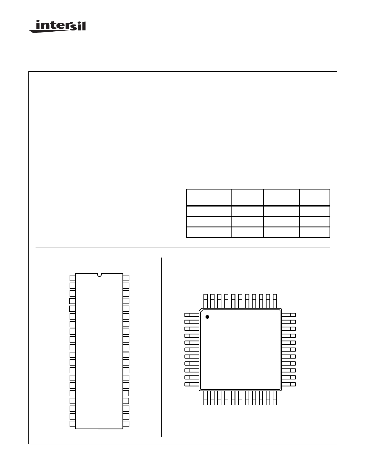
Pinouts
ICL7139, ICL7149 (PDIP)
TOP VIEW
Description
The Intersil ICL7139 and ICL7149 are high performance, low
power, auto-ranging digital multimeter lCs. Unlike other
autoranging multimeter ICs, the ICL7139 and ICL7149
always display the result of a conversion on the correct
range. There is no “range hunting” noticeable in the display.
The unit will autorange between the four different ranges. A
manual switch is used to select the 2 high group ranges. DC
current ranges are 4mA and 40mA in the low current group,
and 400mA and 4A in the high current group. Resistance
measurements are made on 4 ranges, which are divided into
two groups. The low resistance ranges are 4/40kΩ. The high
resistance ranges are 0.4/4MΩ. Resolution on the lowest
range is 1Ω.
Ordering Information
TEMP.
PART NUMBER
ICL7139CPL 0 to 70 40 Ld PDIP E40.6
ICL7149CPL 0 to 70 40 Ld PDIP E40.6
ICL7149CM44 0 to 70 44 Ld MQFP Q44.10x10
RANGE (oC) PACKAGE PKG. NO.
ICL7149 (MQFP)
TOP VIEW
BP2
BP1
V+
V
REF
LOΩ
HIΩ
DEINT
INT 1
C
AZ
C
INT
V/Ω/A
HOLD
1
2
3
4
V-
5
6
7
8
9
10
11
12
13
14
15
16
17
18
19
20
40
39
38
37
36
35
34
33
32
31
30
29
28
27
26
25
24
23
22
21
ADG
3/E3
B3/C
3
F2/DP
3
G2/E
2
A2/D
2
B2/C
2
F1/DP
2
G1/E
1
A1/D
1
B1/C
1
F0/DP
1
G0/E
0
A0/D
0
B0/C
0
LO BAT/V
MΩ/µA
Ω/A
k/m
OSC IN
OSC OUT
A2/D
G2/E
F2/DP
B3/C
ADG
3/E3
POL/AC
NC
BP2
BP1
V+
NC
2
2
/C
/DP
2
1
B
F
44 43 42 41 40
2
2
3
3
1
2
3
4
5
6
7
8
9
10
11
12 13 14 15 16 17
V-
REF
V
| Copyright © Intersil Corporation 1999
POL/AC
COMMON
INT V/Ω
TRIPLE POINT
BEEPER OUT
mA/µA
IΩ-DC/LOΩ-AC
CAUTION: These devices are sensitive to electrostatic discharge; follow proper IC Handling Procedures.
http://www.intersil.com or 407-727-9207
3-33
1
1
1
/E
/D
/C
1
1
1
G
A
B
HIΩ
LOΩ
DEINT
1
0
0
0
/E
/D
0
G
INT 1
0
A
INT V/Ω
/C
0
B
NC
2221201918
AZ
C
TRIPLE POINT
/DP
0
F
39 38 37 36 35 34
COMMON
LO BAT/V
33
32
31
30
29
28
27
26
25
24
23
INT
C
MΩ/µA
Ω/A
k/m
OSC IN
OSC OUT
HOLD
HIΩ-DC/LOΩ-AC
V/Ω/A
mA/µA
BEEPER OUT
NC
File Number 3088.1
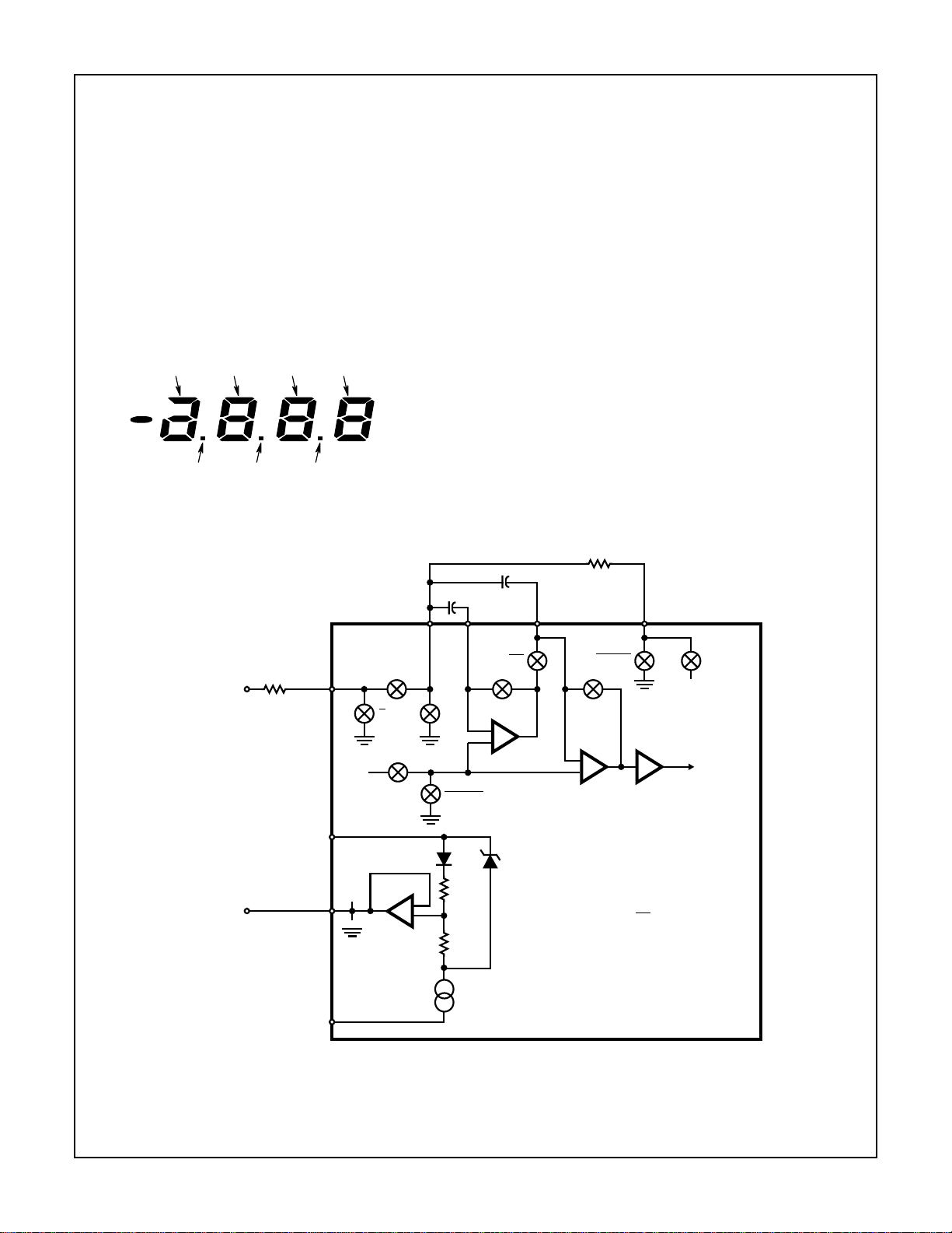
Functional Block Diagram
ICL7139, ICL7149
SWITCHES
CRYSTAL
OSC
DIGITAL COMMON
POWER
SUPPLY
SECTION
V+ V- COM
ANALOG SWITCHES, INTEGRATION
CONTROL LOGIC
INCLUDING
AUTORANGING LOGIC
COUNTERS
ANALOG SECTION
AND COMPARATOR
EXTERNAL
RESISTORS
AND CAPACITORS
BEEPER
DRIVER
DISPLAY
DRIVER
AND
LATCHES
PIEZO
ELECTRIC
BEEPER
DISPLAY
3-34
ICL7139, ICL7149
Absolute Maximum Ratings Thermal Information
Supply Voltage (V+ to V-) . . . . . . . . . . . . . . . . . . . . . . . . . . . . . . 15V
Reference Input Voltage (V
Analog Input Current (IN + Current or IN + Voltage) . . . . . . . 100µA
Clock Input Swing. . . . . . . . . . . . . . . . . . . . . . . . . . . . . . V+ to V+ -3
to COM) . . . . . . . . . . . . . . . . . . . 3V
REF
Operating Conditions
Temperature Range . . . . . . . . . . . . . . . . . . . . . . . . . . . .0oC to 70oC
CAUTION: Stresses above those listed in “Absolute Maximum Ratings” may cause permanent damage to the device. This is a stress only rating and operation
of the device at these or any other conditions above those indicated in the operational sections of this specification is not implied.
NOTE:
1. θJA is measured with the component mounted on an evaluation PC board in free air.
Thermal Resistance (Typical, Note 1) θJA (oC/W)
PDIP Package. . . . . . . . . . . . . . . . . . . . . . . . . . . . . . . 50
MQFP Package. . . . . . . . . . . . . . . . . . . . . . . . . . . . . . 80
Maximum Junction Temperature . . . . . . . . . . . . . . . . . . . . . . . 150oC
Maximum Storage Temperature Range . . . . . . . . . .-65oC to 150oC
Maximum Lead Temperature (Soldering 10s) . . . . . . . . . . . . . 300oC
(MQFP - Lead Tips Only)
Electrical Specifications V+ = 9V, T
Crystal = 120kHz. (See Figure 14)
PARAMETER TEST CONDITIONS MIN TYP MAX UNITS
Zero Input Reading VIN or IIN or RIN = 0.00 -00.0 - +00.0 V, I, Ω
Linearity (Best Straight Line) (Note 6) (Notes 1 and 8) -1
Accuracy DC V, 400V Range Only (Notes 1 and 8) - - ±1 % of RDG ±1
Accuracy DC V, 400V Range Excluded (Notes 1 and 8) - - ±0.30 % of RDG ±1
Accuracy Ω, 4K and 400K Range (Notes 1 and 8) - - ±0.75 % of RDG ±8
Accuracy Ω, 4K and 4M Range (Notes 1 and 8) - - ±1 % of RDG ±9
Accuracy DC I, Unadjusted for Full Scale (Notes 1 and 8) - - ±0.75 % of RDG ±1
Accuracy DC I, Adjusted for Full Scale (Notes 1 and 8) - ±0.2 - % of RDG ±1
Accuracy AC V At 60Hz (Notes 5, 7, and 8) - ±2 - % of RDG
Open Circuit Voltage for Ω Measurements R
Noise VIN = 0, DC V (Note 2, 95% of Time) - 0.1 - LSB
Noise VIN = 0, AC V (Note 2, 95% of Time) - 4 - LSB
Supply Current VIN = 0, DC Voltage Range - 1.5 2.4 mA
Analog Common (with Respect to V+) I
Temperature Coefficient of Analog Common I
Output Impedance of Analog Common I
Backplane/Segment Drive Voltage Average DC < 50mV 2.8 3.0 3.2 V
Backplane/Segment Display Frequency - 75 - Hz
Switch Input Current VIN = V+ to V- (Note 3) -50 - +50 µA
Switch Input Levels (High Trip Point) V+ - 0.5 - V+ V
Switch Input Levels (Mid Trip Point) V- + 3 - V+ - 2.5 V
Switch Input Levels (Low Trip Point) V- - V- + 0.5 V
Beeper Output Drive (Rise or Fall Time) C
Beeper Output Frequency - 2 - kHz
Continuity Detect Range = Low Ω, V
Power Supply Functional Operation V+ to V- 7 9 11 V
Low Battery Detect V+ to V- (Note 4) 6.5 7 7.5 V
NOTES:
1. Accuracy is defined as the worst case deviation from ideal input value including: offset, linearity, and rollover error.
2. Noise is defined as the width of the uncertainty window (where the display will flicker) between two adjacent codes.
3. Applies to pins 17-20.
4. Analog Common falls out of regulation when the Low Battery Detect is asserted, however the ICL7139 and ICL7149 will continue to
operate correctly with a supply voltage above 7V and below 11V.
5. For 50Hz use a 100kHz crystal.
6. Guaranteed by design, not tested.
7. ICL7139 only.
8. RDG = Reading.
= 25oC, V
A
UNKNOWN
COMMON
COMMON
COMMON
LOAD
adjusted for -3.700 reading on DC volts, test circuit as shown in Figure 3.
REF
-
= Infinity - V
< 10µA 2.7 2.9 3.1 V
< 10µA, Temp. = 0oC T o 70oC - -100 - ppm/oC
< 10µA-110Ω
= 10nF - 25 100 µs
= 1.00V - 1.5 - kΩ
REF
REF
+1 Counts
-V
3-35
Timing Waveform
UNDERRANGE
UNDERRANGE
UNDERRANGE
ICL7139, ICL7149
FIRST AUTO ZERO
FIRST INTEGRATE
FIRST DEINTEGRATE
AUTO ZERO
SECOND AUTO ZERO
SECOND INTEGRATE
SECOND DEINTEGRATE
AUTO ZERO
THIRD AUTO ZERO
THIRD INTEGRATE
THIRD DEINTEGRATE
AUTO ZERO
FOURTH AUTO ZERO
FOURTH INTEGRATE
FOURTH DEINTEGRATE
AUTO ZERO
0123456789101112131415161718192021222324
FIGURE 1. LINE FREQUENCY CYCLES (1 CYCLE = 1000 INTERNAL CLOCK PULSES = 2000 OSCILLATION CYCLES)
Pin Descriptions
I/O PIN NUMBER DESCRIPTION
O 1 Segment Driver POL/AC
O 2 Backplane 2
O 3 Backplane 1
I4V+
I5V-
I 6 Reference Input
O7LoΩ
O8HiΩ
I/O 9 Deintegrate
I/O 10 Analog Common
I 11 Int I
I 12 Int V/Ω
I 13 Triple Point
I 14 Auto Zero Capacitor (CAZ)
I 15 Integrate Capacitor (C
O 16 Beeper Output
I17mA/µA
I18Ω/V/A
I19HiΩ DC/LoΩ AC
INT
)
I/O PIN NUMBER DESCRIPTION
I 20 Hold
O 21 Oscillator Out
I 22 Oscillator In
O 23 Segment DRIVER k/m
O 24 Segment Driver Ω/A
O 25 Segment Driver M Ω/µA
O 26 Segment Driver Lo Bat/V
O 27 Segment Driver B0/C
O 28 Segment Driver A0/D
O 29 Segment Driver G0/E
O 32 Segment Driver A1/D
O 33 Segment Driver G1/E
O 34 Segment Driver F1/DP
O 35 Segment Driver B2/C
O 39 Segment Driver B3/C
O 40 Segment Driver ADG3/E
NOTE: For segment drivers, segments are listed as (segment for
backplane 1)/(segment for backplane 2). Example: pin 27; segment
B0 is on backplane 1, segment C0 is on backplane 2.
0
0
0
1
1
1
1
3
3
3-36
ICL7139, ICL7149
Detailed Description
General
The Functional Block Diagram shows the digital section
which includes all control logic, counters, and display drivers .
The digital section is powered by V+ and Digital Common,
which is about 3V below V+. The oscillator is also in the digital section. Normally 120kHz for rejection of 60Hz AC interference and 100kHz for rejection of 50Hz AC should be
used. The oscillator output is divided by two to generate the
internal master clock. The analog section contains the integrator, comparator, reference section, analog buffers, and
several analog switches which are controlled by the digital
logic. The analog section is powered from V+ and V-.
DIGIT 3 2 1 0
e
f
a
g
b kΩ MΩ
c mAV µA
d
LOW
BATT
AC
DP3 DP2 DP1
FIGURE 2. DISPLAY SEGMENT NOMENCLATURE
DC Voltage Measurement
Autozero
Only those portions of the analog section which are used
during DC voltage measurements are shown in Figure 3. As
shown in the timing diagram (Figure 1), each measurement
starts with an autozero (AZ) phase. During this phase, the
integrator and comparator are configured as unity gain buffers and their non-inverting inputs are connected to Common.
The output of the integrator, which is equal to its offset, is
stored on C
the comparator is stored in C
- the autozero capacitor. Similarly, the offset of
AZ
. The autozero cycle equals
lNT
1000 clock cycles which is one 60Hz line cycle with a 120kHz
oscillator, or one 50Hz line cycle with a 100kHz oscillator.
Range 1 Integrate
The ICL7139 and ICL7149 perform a full autorange search
for each reading, beginning with range 1. During the range 1
integrate period, internal switches connect the INT V/Ω
terminal to the Triple Point (Pin 13). The input signal is integrated for 10 clock cycles, which are gated out over a period
of 1000 clock cycles to ensure good normal mode rejection
of AC line interference.
V
COMMON
R
C
AZ
C
TRIPLE
POINT
REF
T
AZ
T
DEINT+
-
+
DEINT+
R
INTV
ANALOG
COMMON
INT V/Ω
V
V+
V-
IN
C
AZ
AZ
-
+
INTEGRATOR
80µA
INT
AZ
6.7V
DEINT
C
INT
COMPARATOR
R
DEINT
DEINT-
AZ
-
+
TO LOGIC SECTION
T = (INT)(AR)(
AR = AUTORANGE CHOPPER
AZ = AUTOZERO
INT = INTEGRATE
AZ)
V
DEINT-
REF
FIGURE 3. DETAILED CIRCUIT DIAGRAM FOR DC VOLTAGE MEASUREMENT
3-37

ICL7139, ICL7149
Range 1 Deintegrate
At the beginning of the deintegrate cycle, the polarity of the
voltage on the integrator capacitor (C
) is checked, and
INT
either the DElNT+ or DElNT- is asserted. The integrator
capacitor C
V
REF/RDElNT
When the voltage on C
V
of the comparator), the comparator output switches, and
OS
the current count is latched. If the C
is then discharged with a current equal to
INT
. The comparator monitors the voltage on C
is reduced to zero (actually to the
INT
voltage zero-crossing
INT
INT
does not occur before 4000 counts have elapsed, the overload flag is set. “OL” (overload) is then displayed on the LCD . If
the latched result is between 360 and 3999, the count is transferred to the output latches and is displayed. When the count
is less than 360, an underrange has occurred, and the
ICL7139 and ICL7149 then switch to range 2 - the 40V scale.
Range 2
The range 2 measurement begins with an autozero cycle
similar to the one that preceded range 1 integration. Range 2
cycle length however, is one AC line cycle, minus 360 clock
cycles. When performing the range 2 cycle, the signal is integrated for 100 clock cycles, distributed throughout one line
cycle. This is done to maintain good normal mode rejection.
Range 2 sensitivity is ten times greater than range 1 (100 vs
10 clock cycle integration) and the full scale voltage of
range 2 is 40V. The range 2 deintegrate cycle is identical to
the range 1 deintegrate cycle, with the result being displayed
only for readings greater than 360 counts. If the reading is
below 360 counts, the ICL7139 and ICL7149 again asserts
the internal underrange signal and proceeds to range 3.
Range 3
The range 3V or 4V full scale measurement is identical to the
range 2 measurement, except that the input signal is integrated during the full 1000 clock cycles (one line frequency
cycle). The result is displayed if the reading is greater than
.
360 counts. Underrange is asserted, and a range 4 measurement is performed if the result is below 360 counts.
Range 4
This measurement is similar to the range 1, 2 and 3 measurements, except that the integration period is 10,000 clock
cycles (10 line cycles) long. The result of this measurement
is transferred to the output latches and displayed even if the
reading is less than 360.
Autozero
After finding the first range for which the reading is above
360 counts, the display is updated and an autozero cycle is
entered. The length of the autozero cycle is variable which
results in a fixed measurement period of 24,000 clock cycles
(24 line cycles).
DC Current
Figure 4 shows a simplified block diagram of the analog
section of the ICL7139 and ICL7149 during DC current
measurement. The DC current measurements are very
similar to DC voltage measurements except: 1) The input
voltage is developed by passing the input current through a
0.1Ω (HI current ranges), or 9.9Ω (LOW current ranges)
LOW I
HIGH I
COMMON
INT I
R
INTI
9.9Ω
0.1Ω
ANALOG
COMMON
V+
V-
R
C
AZ
C
TRIPLE
POINT
I
V
REF
T
AZ
T
DEINT+
-
+
DEINT+
80µA
INT
C
AZ
AZ
AZ
-
+
INTEGRATOR
6.7V
DEINT
C
INT
COMPARATOR
R
DEINT
DEINT-
AZ
-
+
TO LOGIC SECTION
T = (INT)(AR)(
AR = AUTORANGE CHOPPER
AZ = AUTOZERO
INT = INTEGRATE
AZ)
DEINT-
V
REF
FIGURE 4. DETAILED CIRCUIT DIAGRAM FOR DC CURRENT MEASUREMENT
3-38

ICL7139, ICL7149
current sensing resistor; 2) Only those ranges with 1000 and
10,000 clock cycles of integration are used; 3) The R
lNT l
resistor is 1MΩ, rather than the 10MΩ value used for the
R
resistor.
lNT V
By using the lower value integration resistor, and only the 2
most sensitive ranges, the voltage drop across the current
sensing resistor is 40mV maximum on the 4mA and 400mA
ranges; 400mV maximum on the 40mA and 4A scales. With
some increase in noise, these “burden” voltages can be
reduced by lowering the value of both the current sense
resistors and the R
resistor proportionally. The DC
lNT l
current measurement timing diagram is similar to the DC
voltage measurement timing diagram, except in the DC
current timing diagram, the first and second integrate and
deintegrate phases are skipped.
AC Voltage Measurement for ICL7139
As shown in Figure 5, the AC input voltage is applied directly
to the ICL7139 input resistor. No separate AC to DC conversion circuitry is needed. The AC measurement cycle is
begun by disconnecting the integrator capacitor and using
the integrator as an autozeroed comparator to detect the
C
C
AZ
INT
TRIPLE POINT
C
AZ
positive-going zero crossing. Once synchronized to the AC
input, the autozero loop is closed and a normal
integrate/deintegrate cycle begins. The ICL7139 resynchronizes itself to the AC input prior to every reading. Because
diode D4 is in series with the integrator capacitor, only positive current from the integrator flows into the integrator
capacitor, C
. Since the voltage on C
lNT
is proportional to
lNT
the half-wave rectified average AC input voltage, a conversion factor must be applied to convert the reading to RMS.
This conversion factor is π/2√
2 = 1.1107, and the system
clock is manipulated to perform the RMS conversion. As a
result the deintegrate and autozero cycle times are reduced
by 10%.
AC Voltage Measurement for ICL7149
The ICL7149 is designed to be used with an optional AC to
DC voltage converter circuit. It will autorange through two
voltage ranges (400V and 40V), and the AC annunciator is
enabled. A typical averaging AC to DC converter is shown in
Figure 6, while an RMS to DC converter is shown in Figure
7. AC current can also be measured with some simple modifications to either of the two circuits in Figures 6 and 7.
R
DEINT
C
INT
DEINT
~
AC IN
~
R
INTV
COMMON
INT V/Ω
V+
5
ACINT
DEINT
V
REF
D2
D3
D4
DEINT-
AZ
ACS
-
+
COMPARATOR
S = AZ • ACS • ACINT
T = (INT + ACS) AZ AR
ACS = AC SYNC
AR = AUTORANGE CHOPPER
AZ = AUTOZERO
INT = INTEGRATE
D1
ACS
T
T
AZ
-
+
ACINT
AZ
-
+
INTEGRATOR
80µA
6.7V
V-
FIGURE 5. DETAILED CIRCUIT DIAGRAM FOR AC VOLTAGE MEASUREMENT FOR ICL7139 ONLY
3-39

0VAC - 400VAC
0Hz - 1000Hz
V
ICL7139, ICL7149
1.0µF
100kΩ
-
+
V
V
11
20MΩ
IN
100kΩ
50kΩ
4
5
-
ICL7652
+
1
7
10
2
8
43.2kΩ
5kΩ
FULL
SCALE
ADJUST
12
INT (V/Ω)
COM
FIGURE 6. AC VOLTAGE MEASUREMENT USING OPTIONAL AVERAGING CIRCUIT
V
0VAC - 400VAC
50Hz - 1000Hz
IN
20MΩ
4
5
0.1µF
10MΩ
+
V
11
-
ICL7652
+
1
0.1µF
-
V
7
10
2
8
0.1µF
2.2µF
2
+
1
AD736
8
V
7
4
0.1µF
+
3
5
+
10µF
2.2µF
6
ICL7149
10
COMMON
+
5kΩ
12
INT (V/Ω)
FULL
SCALE
ADJUST
+
V
30kΩ
10
COMMON
COM
4.99kΩ
-
V
FIGURE 7. AC VOLTAGE MEASUREMENT USING OPTIONAL RMS CONVERTER CIRCUIT
3-40
ICL7149

ICL7139, ICL7149
C
TRIPLE
POINT
AZ
C
C
AZ
INT
R
DEINT
C
INT
R
DEINT
INT V/Ω
R
INTV
R
X
R
KNOWN 1
R
KNOWN 2
COMMON
LOΩ
LOW Ω
HIΩ
LOW Ω
-
+
-
+
T
T
DEINT+
V
REF
AZ
FIGURE 8. DETAILED CIRCUIT DIAGRAM FOR RATIOMETRIC Ω MEASUREMENT
Ratiometric Ω Measurement
The ratiometric Ω measurement is performed by first
integrating the voltage across an unknown resistor, R
, then
X
effectively deintegrating the voltage across a known resistor
(R
KNOWN1
R
INTV
or R
KNOWN2
of Figure 8). The shunting effect of
does not affect the reading because it cancels exactly
between integration and deintegration. Like the current measurements, the Ω measurements are split into two sets of
ranges. LO Ω measurements use a 10kΩ reference resistor,
and the full scale ranges are 4kΩ and 40kΩ. HI Ω measurements use a 1MΩ reference resistor, and the full scale ranges
are 0.4MΩ and 4MΩ. The measurement phases and timing
are the same as the measurement phases and timing for DC
current except: 1) During the integrate phases the input voltage is the voltage across the unknown resistor R
, and; 2)
X
During the deintegrate phases, the input voltage is the voltage
across the reference resistor R
KNOWN1
or R
KNOWN2
.
Continuity Indication
When the ICL7139 and ICL7149 are in the LO Ω
measurement mode, the continuity circuit of Figure 9 will be
active. When the voltage across R
100mV, the beeper output will be on. When R
the beeper output will be on when R
LOΩ
R
KNOWN
R
UNKNOWN
FIGURE 9. CONTINUITY BEEPER DRIVE CIRCUIT
R
COM
HIΩ
X
-
+
+
-
V
X
is less than approximately
X
is less than 1kΩ.
X
-
+
LOΩ
V
REF
2kHz
VX = 100mV
KNOWN
V+
V+
is 10kΩ,
BEEPER
OUTPUT
DEINT+
AZ
AZ
-
+
INTEGRATOR
T = INT + DEINT
AZ = AUTOZERO
INT = INTEGRATE
AZ
-
+
COMPARATOR
TO LOGIC SECTION
Common Voltage
The analog and digital common voltages of the ICL7139 and
ICL7149 are generated by an on-chip resistor/ zener/ diode
combination, shown in Figure 10. The resistor values are
chosen so the coefficient of the diode voltage cancels the
positive temperature coefficient of the zener voltage. This
voltage is then buffered to provide the analog common and
the digital common voltages. The nominal voltage between
V+ and analog common is 3V. The analog common buffer
can sink about 20mA, or source 0.01mA, with an output
impedance of 10Ω. A pullup resistor to V+ may be used if
more sourcing capability is desired. Analog common may be
used to generate the reference voltage, if desired.
LO BAT
+
-
V+
6.7V
5K
125K
180K
-
+
80µA
3V
ANALOG
COMMON
P
(PIN 10)
+
-
3.1V
+
-
+
LOGIC
SECTION
DIGITAL
COMMON
(INTERNAL)
P
-
0.3V
+
V-
FIGURE 10. ANALOG AND DIGITAL COMMON VOLTAGE
GENERATOR CIRCUIT
Oscillator
The ICL7139 and ICL7149 use a parallel resonant-type
crystal in a Pierce oscillator configuration, as shown in
Figure 11, and requires no other external components. The
crystal eliminates the need to trim the oscillator frequency.
An external signal may be capacitively coupled in OSC IN,
with a signal level between 0.5V and 3V
. Because the
P-P
3-41
ICL7139, ICL7149
OSC OUT pin is not designed to drive large external loads,
loading on this pin should not exceed a single CMOS input.
The oscillator frequency is internally divided by two to generate the ICL7139 and ICL7149 clock. The frequency should
be 120kHz to reject 60Hz AC signals, and 100kHz to reject
50Hz signals.
OSC OUTOSC IN
5M
330K
10pF5pF
FIGURE 11. INTERNAL OSCILLATOR CIRCUIT DIAGRAM
Display Drivers
Figure 12 shows typical LCD Drive waveforms, RMS ON, and
RMS OFF voltage calculations. Duplex multiplexing is used to
minimize the number of connections between the ICL7139
and ICL7149 and the LCD. The LCD has two separate backplanes. Each drive line can drive two individual segments, one
referenced to each backplane. The ICL7139 and ICL7149
3
drive 3
/4 7-segment digits, 3 decimal points, and 11 annunciators. Annunciators are used to indicate polarity, low batter y
condition, and the range in use. Peak drive voltage across the
display is approximately 3V. An LCD with approximately
1.4V
threshold voltage should be used. The third voltage
RMS
level needed for duplex drive waveforms is generated through
an on-chip resistor string. The DC component of the drive
waveforms is guaranteed to be less than 50mV.
Ternary Input
The Ω/ Volts /Amps logic input is a ternar y, or 3-level input.
This input is internally tied to the common voltage through a
high-value resistor, and will go to the middle, or “Volts” state,
when not externally connected. When connected to V-,
approximately 5µA of current flows out of the input. In this
case, the logic level is the “Amps”, or low state. When connected to V+, about 5µA of current flows into the input. Here,
the logic level is the “Ω”, or high state. For other pins, see
Table 2.
TABLE 2. TERNARY INPUTS CONNECTIONS
PIN
NUMBER V+
OPEN
OR COM V-
17 mA µA Test
18 Ω V Amps
19 HiΩ/DC LoΩ/AC Test
20 Hold Auto Test
Component Selection
For optimum performance while maintaining the low-cost
advantages of the ICL7139 and ICL7149, care must be
taken when selecting external components. This section
reviews specifications and performance effects of various
external components.
BACKPLANE
SEGMENT ON
SEGMENT OFF
V
SEGMENT ON
V
SEGMENT OFF
V
V
O
V
O
V
O
2V
O
-2V
V
O
-V
V+
PEAK
PEAK/ 2
DCOM
PEAK
PEAK
(VOLTAGE ACROSS ON SEGMENT)
PEAK
PEAK
(VOLTAGE ACROSS OFF SEGMENT)
PEAK
PEAK
V
V
V
RMS ON → 2.37V
RMS OFF → 1.06V
FIGURE 12. DUPLEXED LCD DRIVE WAVEFORMS
RMS
RMS
PEAK
5
-- -V
PEAK
8
5
-- -V
PEAK
8
= 3V ±10%
ON=
OFF=
3-42

ICL7139, ICL7149
Integrator Capacitor, C
lNT
As with all dual-slope integrating convertors, the integration
capacitor must have low dielectric absorption to reduce
linearity errors. Polypropylene capacitors add undetectable
errors at a reasonable cost, while polystyrene and
polycarbonate may be used in less critical applications. The
ICL7139 and ICL7149 are designed to use a 3.3nF
(0.0033µF) C
an R
lNTV
50Hz line frequency rejection), C
with an oscillator frequency of 120kHz and
lNT
of 10MΩ. With a 100kHz oscillator frequency (for
lNT
and R
affects the
INTV
voltage swing of the integrator. Voltage swing should be as
high as possible without saturating the integrator. Saturation
occurs when the integrator output is within 1V of either V+ or
V -. Integ rator voltage swing should be about ±2V when using
standard component values. For different R
oscillator frequencies the value of C
can be calculated
lNT
lNTV
and
from:
C
Integrate Time()Integrate Current()×
--------------------------------------------------------------------------------------------------- -=
INT
Desired Integrator Swing()
10,000 x 2 x Oscillator Period()0.4V/R
-------------------------------------------------------------------------------------------------------------------------=
2V()
×
INTV
Integrator Resistors
The normal values of the R
lNT V
and R
resistors are
lNT l
10MΩ and 1MΩ respectively. Though their absolute values
are not critical, unless the value of the current sensing resistors are trimmed, their ratio should be 10:1, within 0.05%.
Some carbon composition resistors have a large voltage
coefficient which will cause linearity errors on the 400V scale.
Also, some carbon composition resistors are very noisy. The
class “A” output of the integrator begins to have nonlinearities
if required to sink more than 70µA (the sourcing limit is much
higher). Because R
input impedance of the meter is equal to R
Deintegration Resistor, R
drives a virtual ground point, the
lNT V
DElNT
lNT V
.
Unlike most dual-slope A/D converters, the ICL7139 and
ICL7149 use different resistors for integration and deintegration. R
should normally be the same value as R
DElNT
lNT V
and have the same temperature coefficient. Slight errors in
matching may be corrected by trimming the reference v oltage .
Autozero Capacitor, C
AZ
The CAZ is charged to the integrator’s offset voltage during
the autozero phases, and subtracts that voltage from the
input signal during the integrate phases. The integrator thus
appears to have zero offset voltage. Minimum C
determined by: 1) Circuit leakages; 2) C
AZ
value is
AZ
self-discharge;
3) Charge injection from the internal autozero switches.
To avoid errors, the C
voltage change should be less than
AZ
1/10 of a count during the 10,000 count clock cycle integration period for the 400mV range. These requirements set a
lower limit of 0.047µF for C
value. The upper limit on the value of C
but 0.1µF is the preferred
AZ
is set by the time
AZ
constant of the autozero loop, and the 1 line cycle time
period allotted to autozero. C
may be several 10s of µF
AZ
before approaching this limit.
The ideal C
is a low leakage polypropylene or Teflon
AZ
capacitor. Other film capacitors such as polyester, polystyrene, and polycarbonate introduce negligible errors. If a few
seconds of settling time upon power-up is acceptable, the
C
may be a ceramic capacitor, provided it does not have
AZ
excessive leakage.
Ohm Measurement Resistors
Because the ICL7139 and ICL7149 use a ratiometric ohm
measurement technique, the accuracy of ohm reading is pr imarily determined by the absolute accuracy of the
R
KNOWN1
and R
KNOWN2
. These should normally be 10kΩ
and 1MΩ, with an absolute accuracy of at least 0.5%.
Current Sensing Resistors
The 0.1Ω and 9.9Ω current sensing resistors convert the
measured current to a voltage, which is then measured
using R
the ratio between R
. The two resistors must be closely matched, and
lNT l
and these two resistors must be
lNT l
accurate - normally 0.5%. The 0.1Ω resistor must be capable of handling the full scale current of 4A, which requires it
to dissipate 1.6W.
Continuity Beeper
The Continuity Beeper output is designed to drive a piezoelectric transducer at 2kHz (using a 120kHz crystal), with a
voltage output swing of V+ to V-. The beeper output off state
is at the V+ rail. When crystals with different frequencies are
used, the frequency needed to drive the transducer can be
calculated by dividing the crystal frequency by 60.
Display
The ICL7139 and ICL7149 use a custom, duplexed drive display with range, polarity, and low battery annunciators. With
a 3V peak display voltage, the RMS ON voltage will be
2.37V minimum; RMS OFF voltage will be 1.06V maximum.
Because the display voltage is not adjustable, the display
should have a 10% ON threshold of about 1.4V. Most display
manufacturers supply a graph that shows contrast versus
RMS drive voltage. This graph can be used to determine
what the contrast ratio will be when driven by the ICL7139
,
and ICL7149. Most display thresholds decrease with
increasing temperature. The threshold at the maximum
operating temperature should be checked to ensure that the
“off” segments will not be turned “on” at high temperatures.
Crystal
The ICL7139 and ICL7149 are designed to use a parallel
resonant 120kHz or 100kHz crystal with no additional external components. The R
parameter should be less than
S
25kΩ to ensure oscillation. Initial frequency tolerance of the
crystal can be a relatively loose 0.05%.
Switches
Because the logic input draws only about 5µA, switches
driving these inputs should be rated for low current, or “dry”
operations. The switches on the e xternal inputs must be ab le
to reliably switch low currents, and be able to handle
voltages in excess of 400V
AC
.
3-43

ICL7139, ICL7149
Reference Voltage Source
A voltage divider connected to V+ and Common is the simplest source of reference voltage. While minimizing external
component count, this approach will provide the same voltage tempco as the ICL7139 and ICL7149 Common - about
100PPM/
o
C. To improve the tempco, an ICL8069 bandgap
reference may be used (see Figure 13). The reference voltage source output impedance must be ≤ R
V+
10K
10M
ICL8069
10K
1M
FIGURE 13. EXTERNAL VOLTAGE REFERENCE CONNECTION
TO ICL7139 AND ICL7149
10M
TRIPLE POINT
DEINTEGRATE
INTEGRATE VOLT/Ω
INTEGRATE CURRENT
REFERENCE INPUT
ANALOG COMMON
10MΩ
DElNT
0.1µF
/4000.
EXTERNAL
REFERENCE
3.3nF
120kHz
CRYSTAL
Applications, Examples, and Hints
3
A complete autoranging 3
/4 digit multimeter is shown in
Figure 14. The following sections discuss the functions of
specific components and various options.
Meter Protection
The ICL7139 and ICL7149 and their external circuitry should
be protected against accidental application of 110/220V AC
line voltages on the Ω and current ranges. Without the necessary precautions, both the ICL7139 and ICL7149 and their
external components could be damaged under such fault
conditions. For the current ranges, fast-blow fuses should be
used between S5A in Figure 14 and the 0.1Ω and 9.9Ω
shunt resistors. For the Ω ranges, no additional protection
circuitry is required. However, the 10kΩ resistor connected
to pin 7 must be able to dissipate 1.2W or 4.8W for short
periods of time during accidental application of 110V or
220V
line voltages respectively.
AC
21 22
C
OSC
INT
AZ
OUT
DISPLAY
OUTPUTS
BEEPER
ICL7139
ICL7149
HIΩ-DC/LOΩ-AC
INPUTS
V/Ω
A
COMMON
V+
µA
S4A
S5A
mA
V+
13 14 15
C
TRIPLE
POINT
9
12
7
8
11
10
18
17
DEINT
INT (V/Ω)
LOΩ
HIΩ
INT (I)
COMMON
V/Ω/A
mA/µA
10MΩ
V
10kΩ
Ω
A
1MΩ
mA
1MΩ
9.9Ω
0.1Ω
2W
V
S4B
A
µA
30K50K
Ω
V-
NOTES:
1. Crystal is a Statek or SaRonix CX-IV type.
2. Multimeter protection components have not been shown.
3. Display is from LXD, part number 38D8R02H (or Equivalent).
4. Beeper is from muRata, part number PKM24-4A0 (or Equivalent).
OSC
IN
DRIVE
V+
V
REF
HOLD
LO BAT
1-3
23-40
AC
16
4
+
1µF
5
V-
6
19
20
ON/OFF
S3
S3
BEEPER
+
9V
BATTERY
-
S1
V+
V+
S2 CLOSED: HIΩ-DC
S3 CLOSED: HOLD READING
10kΩ
4.7µF
TANT
mAVµA
kΩMΩ
PIN 4
10kΩ
+
ICL8069
PIN 10
FIGURE 14. BASIC MULTIMETER APPLICATION CIRCUIT FOR ICL7139 AND ICL7149
3-44

ICL7139, ICL7149
Printed Circuit Board Layout Considerations
Particular attention must be paid to rollover performance,
leakages, and guarding when designing the PCB for a
ICL7139 and ICL7149 based multimeter.
14 15131211109
FIGURE 15. PC BOARD LAYOUT
Rollover Performance, Leakages, and Guarding
Because the ICL7139 and ICL7149 system measures very
low currents, it is essential that the PCB have low leakage.
Boards should be properly cleaned after soldering. Areas of
particular impor tance are: 1) The INT V/Ω and INT l Pins; 2)
The Triple Point; 3) The R
and the CAZ pins.
DElNT
The conversion scheme used by the ICL7139 and ICL7149
changes the common mode voltage on the integrator and
the capacitors C
and C
AZ
during a positive deintegrate
lNT
cycle. Stray capacitance to ground is charged when this
occurs, removing some of the charge on C
and causing
lNT
rollover error . Rollo v er error increases about 1 count f or each
picofarad of capacitance between C
or the Triple Point
AZ
and ground, and is seen as a zero offset for positive voltages. Rollover error is not seen as gain error.
The rollover error causes the width of the +0 count to be
larger than normal. The ICL7139 and ICL7149 will thus read
zero until several hundred microvolts are applied in the positive direction. The ICL7139 and ICL7149 will read -1 when
approximately -100µV is applied.
The rollover error can be minimized by guarding the Triple
Point and C
nodes with a trace connected to the C
AZ
lNT
pin,
(see Figure 15) which is driven by the output of the integrator. Guarding these nodes with the output of the integrator
reduces the stray capacitance to ground, which minimizes
the charge error on C
and CAZ. If possible, the guarding
lNT
should be used on both sides of the PC board.
Stray Pickup
While the ICL7139 and ICL7149 have excellent rejection of
line frequency noise and pickup in the DC ranges, any stray
coupling will affect the AC reading. Generally, the analog circuitry should be as close as possible to the ICL7139 and
ICL7149. The analog circuitry should be removed or
shielded from any 120V AC power inputs, and any AC
sources such as LCD drive waveforms. Keeping the analog
circuit section close to the ICL7139 and ICL7149 will also
help keep the area free of any loops, thus reducing magnetically coupled interference coming from power transformers,
or other sources.
All Intersil semiconductor products are manufactured, assembled and tested under ISO9000 quality systems certification.
Intersil products are sold by description only. Intersil Corporation reserves the right to make changes in circuit design and/or specifications at any time without
notice. Accordingly, the reader is cautioned to verify that data sheets are current before placing orders. Information furnished by Intersil is believed to be accurate
and reliable. However, no responsibility is assumed by Intersil or its subsidiaries for its use; nor for any infringements of patents or other rights of third parties which
may result from its use. No license is granted by implication or otherwise under an y patent or patent rights of Intersil or its subsidiaries.
For information regarding Intersil Corporation and its products, see web site http://www.intersil.com
3-45
 Loading...