

Page 1
TM
ICL7135
Data Sheet December 2000
41/2 Digit, BCD Output, A/D Converter
The Intersil ICL7135 precision A/D converter, with its
multiplexed BCD output and digit drivers, combines dualslope conversion reliability with ±1in 20,000 count accuracy
and is ideally suited for the visual display DVM/DPM market.
The 2.0000V full scale capability, auto-zero, and autopolarity are combined with true ratiometric operation, almost
ideal differential linearity and true differential input. All
necessary active devices are contained on a single CMOS
lC, with the exception of display drivers, reference, and a
clock.
The ICL7135 brings together an unprecedented combination
of high accuracy, versatility, and true economy. It features
auto-zero to less than 10µV, zero drift of less than 1µV/
input bias current of 10pA (Max), and rollover error of less
than one count. The versatility of multiplexed BCD outputs is
increased by the addition of several pins which allow it to
operate in more sophisticated systems. These include
STROBE, OVERRANGE, UNDERRANGE, RUN/HOLD and
BUSY lines, making it possible to interface the circuit to a
microprocessor or UART.
o
C,
File Number 3093.2
Features
• Accuracy Guaranteed to ±1 Count Over Entire ±20000
Counts (2.0000V Full Scale)
• Guaranteed Zero Reading for 0V Input
• 1pA Typical Input Leakage Current
• True Differential Input
• True Polarity at Zero Count for Precise Null Detection
• Single Reference Voltage Required
• Overrange and Underrange Signals Available for AutoRange Capability
• All Outputs TTL Compatible
• Blinking Outputs Gives Visual Indication of Overrange
• Six Auxiliary Inputs/Outputs are Available for Interfacing to
UARTs , Microprocessors , or Other Circuitry
• Multiplexed BCD Outputs
Ordering Information
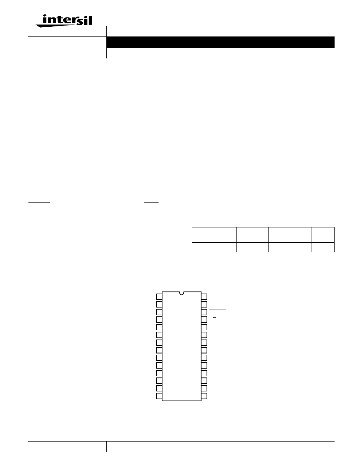
Pinout
REFERENCE
ANALOG COMMON
INT OUT
AZ IN
BUFF OUT
REF CAP -
REF CAP +
IN LO
IN HI
V+
(MSD) D5
(LSB) B1
B2
TEMP.
PART NUMBER
ICL7135CPI 0 to 70 28 Ld PDIP E28.6
ICL7135
(PDIP)
TOP VIEW
28
V-
1
2
3
4
5
6
7
8
9
10
11
12
13
14
UNDERRANGE
27
OVERRANGE
STROBE
26
H
25
R/
24
DIGITAL GND
23
POL
CLOCK IN
22
21
BUSY
20
(LSD) D1
D2
19
18
D3
17
D4
16
(MSB) B8
15
B4
RANGE (oC) PACKAGE
PKG.
NO.
1
1-888-INTERSIL or 321-724-7143 | Intersil and Design is a trademark of Intersil Corporation. | Copyright © Intersil Corporation 2000
CAUTION: These devices are sensitive to electrostatic discharge; follow proper IC Handling Procedures.
Page 2
Typical Application Schematic
ICL7135
V
REF
ANALOG
GND
100kΩ
SIGNAL
INPUT
SET V
IN
REF
100kΩ
= 1.000V
0.47µF
1µF
100K
0.1µF
-5V
27Ω
100kΩ
1µF
+5V
1
2
3
4
5
6
7
8
9
10
11
12
13
14
ICL7135
28
27
26
25
24
23
22
21
20
19
18
17
16
15
CLOCK IN
120kHz
0V
TRANSISTORS
6
SEVEN
DECODE
SEG.
ANODE
DRIVER
DISPLAY
2
Page 3
ICL7135
Absolute Maximum Ratings Thermal Information
Supply Voltage V+ . . . . . . . . . . . . . . . . . . . . . . . . . . . . . . . . . . . +6V
V- . . . . . . . . . . . . . . . . . . . . . . . . . . . . . . . . . . . -9V
Analog Input Voltage (Either Input) (Note 1) . . . . . . . . . . . . V+ to V-
Reference Input Voltage (Either Input). . . . . . . . . . . . . . . . . V+ to V-
Clock Input Voltage . . . . . . . . . . . . . . . . . . . . . . . . . . . . . GND to V+
Operating Conditions
Temperature Range. . . . . . . . . . . . . . . . . . . . . . . . . . . . 0oC to 70oC
CAUTION: Stresses above those listed in “Absolute Maximum Ratings” may cause permanent damage to the device. This is a stress only rating and operation of the
device at these or any other conditions above those indicated in the operational sections of this specification is not implied.
NOTES:
1. Input voltages may exceed the supply voltages provided the input current is limited to +100µA.
2. θJA is measured with the component mounted on a low effective thermal conductivity test board in free air. See Tech Brief TB379 for details.
Thermal Resistance (Typical, Note 2) . . . . . . . . . . . . . θJA (oC/W)
PDIP Package . . . . . . . . . . . . . . . . . . . . . . . . . . . . . 55
Maximum Junction Temperature . . . . . . . . . . . . . . . . . . . . . . .150oC
Maximum Storage Temperature Range. . . . . . . . . . -65oC to 150oC
Maximum Lead Temperature (Soldering 10s) . . . . . . . . . . . . .300oC
Electrical Specifications V+ = +5V, V- = -5V, T
PARAMETER TEST CONDITIONS
= 25oC, f
A
Set for 3 Readings/s, Unless Otherwise Specified
CLK
MIN TYP MAX UNITS
ANALOG (Notes 3, 4)
Zero Input Reading V
Ratiometric Error (Note 4) V
= 0V, V
lN
= V
lN
Linearity Over ± Full Scale (Error of Reading from Best Straight Line) -2V ≤ V
Differential Linearity (Difference Between Worse Case Step of
-2V ≤ V
= 1.000V -00000 +00000 +00000 Counts
REF
= 1.000V -3 0 +3 Counts
REF
≤ +2V - 0.5 1 LSB
IN
≤ +2V - 0.01 - LSB
IN
Adjacent Counts and Ideal Step)
Rollover Error (Difference in Reading for Equal Positive and
≡ +VlN≈ 2V - 0.5 1 LSB
-V
lN
Negative Voltage Near Full Scale)
Noise (Peak-to-Peak Value Not Exceeded 95% of Time), e
Input Leakage Current, I
ILK
N
Zero Reading Drift (Note 7) V
Scale Factor Temperature Coefficient, T
(Notes 5 and 7) VlN = +2V, 0oC to 70oC
C
VlN = 0V, Full scale = 2.000V - 15 - µV
VlN = 0V - 1 10 pA
= 0V, 0oC to 70oC - 0.5 2 µV/oC
lN
- 2 5 ppm/oC
Ext. Ref. 0ppm/oC
DIGITAL INPUTS
Clock In, Run/
Hold (See Figure 2) V
V
I
I
INH
INL
INL
INH
VIN = 0V - 0.02 0.1 mA
VIN = +5V - 0.1 10 µA
2.8 2.2 - V
- 1.6 0.8 V
DIGITAL OUTPUTS
All Outputs, V
B1, B2, B4, B8, D1, D2, D3, D4, D5, V
BUSY,
OL
OH
STROBE, OVERRANGE, UNDERRANGE, POLARITY, V
IOL = 1.6mA - 0.25 0.40 V
IOH = -1mA 2.4 4.2 - V
OHIOH
= -10µA 4.9 4.99 - V
SUPPLY
+5V Supply Range, V+ +4 +5 +6 V
-5V Supply Range, V- -3 -5 -8 V
+5V Supply Current, I+ fC = 0 - 1.1 3.0 mA
-5V Supply Current, I- f
Power Dissipation Capacitance, C
PD
= 0 - 0.8 3.0 mA
C
vs Clock Frequency - 40 - pF
CLOCK
Clock Frequency (Note 6) DC 2000 1200 kHz
NOTES:
1
3. Tested in 4
4. Tested with a low dielectric absorption integrating capacitor, the 27Ω INT OUT resistor shorted, and R
/2 digit (20.000 count) circuit shown in Figure 3. (Clock frequency 120kHz.)
= 0. See Component Value Selection
lNT
Discussion.
5. The temperature range can be extended to 70oC and beyond as long as the auto-zero and reference capacitors are increased to absorb the
higher leakage of the ICL7135.
6. This specification relates to the clock frequency range over which the lCL7135 will correctly perform its various functions See “Max Clock
Frequency” section for limitations on the clock frequency range in a system.
7. Parameter guaranteed by design or characterization. Not production tested.
3
Page 4
ICL7135
V
REF
100kΩ
ANALOG
GND
SIGNAL
INPUT
IN
100kΩ
REF
0.47µF
1µF
0.1µF
= 1.000V
-5V
27Ω
100kΩ
1µF
+5V
V-
1
REF
2
3
ANALOG GND
INT OUT
4
A-Z IN
5
BUF OUT
6
REF CAP 1
7
REF CAP 2
8
IN LO-
9
IN HI+
10
V+
11
MSD D5
12
LSB B1
13
B2
14
ICL7135
UNDERRANGE
OVERRANGE
STROBE
RUN/
HOLD
DIGITAL GND
POLARITY
CLOCK IN
BUSY
LSD DI
MSB B8
D2
D3
D4
B4
28
27
26
25
24
0V
23
CLOCK
22
IN
120kHz
21
20
19
18
17
16
15
PAD
SET V
100K
FIGURE 1. ICL7135 TEST CIRCUIT FIGURE 2. ICL7135 DIGITAL LOGIC INPUT
+
V
DIG GND
IN HI
ANALOG
COMMON
IN LO
C
REF
C
REF+
10
INT
AZ
3
INT
9
REF HI
2
87
AZ
DE(-) DE(+)
DE(+) DE(-)
A/Z, DE(±), ZI
A/Z
C
REF
-
V
INPUT
HIGH
1
R
INT
BUFFER
-
+
ZI
C
AZ
+
V
AUTO
ZERO
INTEGRAT OR
AZ
COMP ARATOR
INPUT
LOW
C
INT
INT
45611
-
+
+
ZEROCROSSING
DETECTOR
POLARITY
F/F
FIGURE 3. ANALOG SECTION OF ICL7135
4
Page 5
ICL7135
Detailed Description
Analog Section
Figure 3 shows the Block Diagram of the Analog Section for
the ICL7135. Each measurement cycle is divided into four
phases. They are (1) auto-zero (AZ), (2) signal-integrate
(INT), (3) de-integrate (DE) and (4) zero-integrator (Zl).
Auto-Zero Phase
During auto-zero, three things happen. First, inputhigh and low
are disconnected from thepins and internally shorted to analog
COMMON. Second, the reference capacitor is charged to the
reference voltage. Third, a feedback loop is closed around the
system to charge the auto-zero capacitor C
for offset voltages in the b uff er amplifier, integrator , and
comparator. Since the comparator is included in the loop, the
AZ accuracy is limited only by the noise of the system. In any
case, the offset referred to the input is less than 10µV.
Signal Integrate Phase
During signal integrate, the auto-zero loop is opened, the
internal short is removed, and the internal input high and low
are connected to the external pins. The converter then
integratesthe differential voltage between IN HIand IN LO fora
fixed time. This diff erential v oltage can be within a wide
common mode range; within one volt of either supply .If, on the
other hand, the input signal has no return with respect to the
converter power supply,IN LO can be tied to analog COMMON
to establish the correct common-mode voltage. At the end of
this phase, the polarity of the integrated signal is latched into
the polarity F/F.
De-Integrate Phase
The third phase is de-integrate or reference integrate. Input
low is internally connected to analog COMMON and input
high is connected across the previously charged reference
capacitor. Circuitry within the chip ensures that the capacitor
will be connected with the correct polarity to cause the integrator output to return to zero. The time required for the output to return to zero is proportional to the input signal.
Specifically the digital reading displayed is:
V
IN
---------------
OUTPUT COUNT 10,000
=
V
.
REF
Zero Integrator Phase
The final phase is zero integrator. First, input low is shorted
to analog COMMON. Second, a feedback loop is closed
around the system to input high to cause the integrator
output to return to zero. Under normal condition, this phase
lasts from 100 to 200 clock pulses, but after an overrange
conversion, it is extended to 6200 clock pulses.
to compensate
AZ
Howev er, since the integrator also swings with the common
mode voltage, care must be exercisedto assure theintegrator
output does not saturate. A worst case condition would be a
large positive common-mode voltage with a near full scale
negative differential input v oltage. The negative input signal
drives the integrator positive when most of its swing has been
used up by the positive common mode voltage. For these
critical applications the integrator swing can be reduced to
less than the recommended 4V full scale swing with some
loss of accuracy. The integrator output can swing within 0.3V
of either supply without loss of linearity.
Analog COMMON
Analog COMMON is used as the input low return during autozero and de-integrate. If IN LO is diff erent from analog
COMMON, a common mode voltage exists in the system and
is taken care of by the excellent CMRR of the converter.
Howev er, in most applications IN LO will be set at a fixed
known voltage (power supply common for instance). In this
application, analog COMMON should be tied to the same
point, thus removing the common mode voltage from the
converter. The reference voltage is referenced to analog
COMMON.
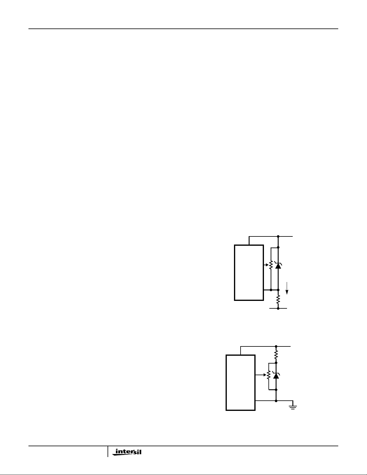
Reference
The reference input must be generated as a positive voltage
with respect to COMMON, as shown in Figure 4.
V+
6.8V
ZENER
V-
V+
6.8kΩ
ICL8069
1.2V
REFERENCE
I
Z
ICL7135
COMMON
V+
REF HI
ICL7135
REF HI
FIGURE 4A.
20kΩ
Differential Input
The input can accept differentialvoltages anywhere within the
common mode range of the input amplifier; or specifically
from 0.5V below the positive supply to 1V abov e the negative
supply. In this range the system has a CMRR of 86dB typical.
5
COMMON
FIGURE 4B.
FIGURE 4. USING AN EXTERNAL REFERENCE
Page 6

ICL7135
Digital Section
Figure 5 shows the Digital Section of the ICL7135. The
ICL7135 includes several pins which allow it to operate
conveniently in more sophisticated systems. These include:
Run/
HOLD (Pin 25)
When high (or open) the A/D will free-run with equally
spaced measurement cycles every 40,002 clock pulses. If
taken low, the converter will continue the full measurement
cycle that it is doing and then hold this reading as long as
R/
H is held low. A short positive pulse (greater than 300ns)
will now initiate a new measurement cycle, beginning with
between 1 and 10,001 counts of auto zero. If the pulse
occurs before the full measurement cycle (40,002 counts) is
completed, it will not be recognized and the converter will
simply complete the measurement it is doing. An external
indication that a full measurement cycle has been completed
is that the first strobe pulse (see below) will occur 101 counts
after the end of this cycle. Thus, if Run/
HOLD is low and has
been low for at least 101 counts, the converter is holding and
ready to start a new measurement when pulsed high.
STROBE (Pin 26)
This is a negative going output pulse that aids in transferring
the BCD data to external latches, UARTs, or
microprocessors. There are 5 negative going
STROBE
pulses that occur in the center of each of the digit drive
pulses and occur once and only once foreach measurement
cycle starting 101 clock pulses after the end of the full
measurement cycle. Digit 5 (MSD) goes high at the end of
the measurement cycle and stays on for 201 counts. In the
center of this digit pulse (to avoid race conditions between
changing BCD and digit drives) the first
negative for
1
/2clock pulse width. Similarly,after digit 5, digit
STROBE pulse goes
4 goes high (for 200 clock pulses) and 100 pulses later the
STROBE goes negative for the second time. This continues
through digit 1 (LSD) when the fifth and last
STROBE pulse
is sent. The digit drive will continue to scan (unless the
previous signal was overrange) but no additional
STROBE
pulses will be sent until a new measurement is available.
BUSY (Pin 21)
BUSY goes high at the beginning of signal integrate and
stays high until the first clock pulse after zero crossing (or
after end of measurement in the case of an overrange).The
internal latches are enabled (i.e., loaded) during the first
clock pulse after busyand are latched at the end of this clock
pulse. The circuit automatically reverts to auto-zero when
not BUSY, so it may also be considered a (
Zl + AZ) signal. A
very simple means for transmitting the data down a single
wire pair from a remote location would be to AND BUSY with
clock and subtract 10,001 counts from the number of pulses
received - as mentioned previously there is one “NO-count”
pulse in each reference integrate cycle.
OVERRANGE (Pin 27)
This pin goes positive when the input signal exceeds the
range (20,000) of the converter. The output F/F is set at the
end of BUSY and is reset to zero at the beginning of
reference integrate in the next measurement cycle.
UNDERRANGE (Pin 28)
This pin goes positive when the reading is 9% of range or
less. The output F/F is set at the end of BUSY (if the new
reading is 1800 or less) and is reset at the beginning of
signal integrate of the next reading.
POLARlTY (Pin 23)
This pin is positive for a positive input signal. It is valid even
fora zero reading. In other words,+0000 means the signal is
positive but less than the least significant bit. The converter
can be used as a null detector by forcing equal frequency of
(+) and (-) readings. The null atthis point shouldbe less than
0.1 LSB. This output becomes valid at the beginning of
reference integrate and remains correct until it is revalidated
for the next measurement.
ANALOG
SECTION
ZERO
CROSS.
DET.
+
POLARITY
V
11
POLARITY
DIGITAL CLOCK RUN/ BUSYOVER
23
FF
24 22 2725 28 26 21
GND IN
FIGURE 5. DIGITAL SECTION OF THE ICL7135
LATCH
6
D5
12
MSB LSB
HOLD
17
LATCH LATCH LATCH
CONTROL LOGIC
RANGE RANGE
18
MULTIPLEXER
LATCH
COUNTERS
UNDER
STROBE
19 20
D1D2D3D4
13
B1
14
B2
15
B4
16
B8
Page 7

ICL7135
Digit Drives (Pins 12, 17, 18, 19 and 20)
Each digit driveis a positive goingsignal that lasts for200 clock
pulses. The scan sequence is D5 (MSD), D4, D3, D2, and D1
(LSD). All five digits are scanned and this scan is continuous
unless an overrange occurs. Then all digit driv es are b lanked
from the end of the strobe sequence until the beginning of
ReferenceIntegratewhen D5 will start the scan again.This can
give a blinking displa y as a visual indication of overrange.
BCD (Pins 13, 14, 15 and 16)
The Binary coded Decimal bits B8, B4, B2, and B1 are
positive logic signals that go on simultaneously with the digit
driver signal.
Component Value Selection
For optimum performance of the analog section, care must
be taken in the selection of values for the integratorcapacitor
and resistor, auto-zero capacitor, reference voltage, and
conversion rate. These values must be chosen to suit the
particular application.
Integrating Resistor
The integrating resistor is determined by the full scale input
voltage and the output current of the buffer used to charge
the integrator capacitor. Both the buffer amplifier and the
integrator have a class A output stage with 100µA of
quiescent current. They can supply 20µA of drive current
with negligible non-linearity. Values of 5µA to 40µA give
good results, with a nominal of 20µA, and the exact value of
integrating resistor may be chosen by:
R
full scale voltage
------------------------------------------- -=
INT
20µA
Integrating Capacitor
The product of integrating resistor and capacitor should be
selected to give the maximum voltage swing which ensures
that the tolerance built-up will not saturate the integrator
swing (approx. 0.3V from either supply). For ±5V supplies
and analog COMMON tied to supply ground, a ±3.5V to ±4V
full scale integrator swing is fine, and 0.47µF is nominal. In
general, the value of C
10,000 clock period×
C
--------------------------------------------------------------------------------- -
=
INT
integrator output voltage swing
(10,000) (clock period) (20µA)
---------------------------------------------------------------------------------=
integrator output voltage swing
A very important characteristic of the integrating capacitor is
that it has low dielectric absorption to prevent roll-over or
ratiometric errors. A good test for dielectric absorption is to
use the capacitor with the input tied to the reference.
This ratiometric condition should read half scale 0.9999, and
any deviation is probably due to dielectric absorption.
Polypropylene capacitors give undetectable errors at
reasonable cost. Polystyrene and polycarbonate capacitors
may also be used in less critical applications.
.
is given by:
lNT
,
×
I
INT
.
Auto-Zero and Reference Capacitor
The physical size of the auto-zero capacitor has an influence
on the noise of the system. A larger capacitor value reduces
system noise. A larger physical size increases system noise.
The reference capacitor should be large enough such that
stray capacitance to ground from its nodes is negligible.
The dielectric absorption of the reference cap and auto-zero
cap are only important at power-on or when the circuit is
recovering from an overload. Thus, smaller or cheaper caps
can be used here if accurate readings are not required for
the first few seconds of recovery.
Reference Voltage
The analog input required to generate a full scale output is
V
lN
= 2V
REF
.
The stability of the reference voltage is a major factor in the
overallabsolute accuracy of the converter.For this reason, it
is recommended that a high quality reference be used where
high-accuracy absolute measurements are being made.
Rollover Resistor and Diode
A small rollover error occurs in the ICL7135, but this can be
easily corrected by adding a diode and resistor in series
between the INTegrator OUTput and analog COMMON or
ground. The value shown in the schematics is optimum for
the recommended conditions, but if integrator swing or clock
frequency is modified, adjustment may be needed. The
diode can be any silicon diode such as 1N914. These
components can be eliminated if rollover error is not
important and may be altered in value to correct other
(small) sources of rollover as needed.
Max Clock Frequency
The maximum conversion rate of most dual-slope A/D
converters is limited by the frequency response of the
comparator. The comparator in this circuit follows the
integrator ramp with a 3µs delay, and at a clock frequency of
160kHz (6µs period) half of the first referenceintegrate clock
period is lost in delay. This means that the meter reading will
change from 0 to 1 with a 50µV input, 1 to 2 with a 150µV
input, 2 to 3 with a 250µV input, etc. This transition at midpoint is considered desirable by most users; however, if the
clock frequency is increased appreciably above160kHz, the
instrument will flash “1” on noise peaks even when the input
is shorted.
For many dedicated applications where the input signal is
always of one polarity, the delay of the comparator need not
be a limitation. Since the non-linearity and noise do not
increase substantially with frequency, clock rates of up to
~1MHz may be used. For a fixed clock frequency, the extra
count or counts caused by comparator delay will be constant
and can be subtracted out digitally.
The clock frequency may be extended above 160kHz
without this error, however, by using a low value resistor in
7
Page 8

ICL7135
series with the integrating capacitor. The effect of the
resistor is to introduce a small pedestal voltage on to the
integrator output at the beginning of the reference integrate
phase. By careful selection of the ratio between this resistor
and the integrating resistor (a few tens of ohms in the
recommended circuit), the comparator delay can be
compensated and the maximum clock frequency extended
by approximately a factor of 3. At higher frequencies, ringing
and second order breaks will cause significant nonlinearities in the first few counts of the instrument. See
Application Note AN017.
The minimum clock frequency is established by leakage on
the auto-zero and reference caps. With most devices,
measurement cycles as long as 10s give no measurable
leakage error.
To achieve maximum rejection of 60Hz pickup, the signal
integrate cycle should be a multiple of 60Hz. Oscillator
frequencies of 300kHz, 200kHz, 150kHz, 120kHz, 100kHz,
40kHz, 33
rejection, oscillator frequencies of 250kHz, 166
1
/3kHz, etc. should be selected. For 50Hz
2
/3kHz,
125kHz, 100kHz, etc. would be suitable. Note that 100kHz
(2.5 readings/sec) will reject both 50Hz and 60Hz.
The clock used should be free from significant phase or
frequency jitter. Several suitable low-cost oscillators are
shown in the Typical Applications section. The multiplexed
output means that if the display takes significant current from
the logic supply, the clock should have good PSRR.
Zero-Crossing Flip-Flop
The flip-flop interrogates the data once every clock pulse
after the transients of the previous clock pulse and half-clock
pulse have died down. False zero-crossings caused by clock
pulses are not recognized. Of course, the flip-flop delays the
true zero-crossing by up to one count in every instance, and
if a correction were not made, the display would always be
one count too high. Therefore, the counter is disabled for
one clock pulse at the beginning of phase 3. This one-count
delay compensates for the delay of the zero-crossing
flip-flop, and allows the correct number to be latched into the
display. Similarly, a one-count delay at the beginning of
phase 1 gives an overload display of 0000 instead of 0001.
No delay occurs during phase 2, so that true ratiometric
readings result.
Evaluating The Error Sources
Errors from the “ideal” cycle are caused by:
INTEGRATOR
OUTPUT
BUSY
OVER-RANGE
WHEN APPLICABLE
UNDER-RANGE
WHEN APPLICABLE
DIGIT SCAN
FOR OVER-RANGE
STROBE
DIGIT SCAN
FOR OVER-RANGE
FIGURE 6. TIMING DIAGRAM FOR OUTPUTS
AUTO
SIGNAL
ZERO
10,001/
COUNTS
EXPANDED SCALE
1000
COUNTS
INT.
10,000/
COUNTS
FULL MEASUREMENT
CYCLE 40,002 COUNTS
BELOW
†/
REF INT ONE COUNT LONGER
AUTO ZERO
SIGNAL INTEGRATE
D5
D4
D3
D2
D1
REFERENCE
INTEGRATE
20,001/
COUNTS MAX.
D5
D4
D3
D2
D1
†FIRST D5 OF AZ AND
REFERENCE
INTEGRATE
1. Capacitor droop due to leakage.
2. Capacitor voltage change due to charge “suck-out” (the
reverse of charge injection) when the switches turn off.
3. Non-linearity of buffer and integrator.
4. High-frequency limitations of buffer,integrator,and
comparator.
5. Integrating capacitor non-linearity (dielectric absorption).
6. Charge lost by C
7. Charge lost by C
in charging C
REF
and C
AZ
to charge C
lNT
STRAY
.
STRAY
.
Each error is analyzed for its error contribution to the
converter in application notes listed on the back page,
specifically Application Note AN017 and Application Note
AN032.
Noise
The peak-to-peak noise around zero is approximately 15µV
(peak-to-peak value not exceeded 95% ofthe time). Near full
scale, this value increases to approximately 30µV. Much of
the noise originates in the auto-zeroloop,and is proportional
to the ratio of the input signal to the reference.
Analog And Digital Grounds
Extreme care must be taken to avoid ground loops in the
layout of ICL7135 circuits, especially in high-sensitivity
circuits. It is most important that return currents from digital
loads are not fed into the analog ground line.
8
Page 9

ICL7135
Power Supplies
The ICL7135 is designed to work from ±5V supplies.
However, in selected applications no negative supply is
required. The conditions to use a single +5V supply are:
1. The input signal can be referenced to the center of the
common mode range of the converter.
2. The signal is less than ±1.5V.
See “differential input” for a discussion of the effects this will
have on the integrator swing without loss of linearity.
Typical Applications
The circuits which follow show some of the wide variety of
possibilities and serve to illustrate the exceptional versatility
of this A/D converter.
Figure 7 showsthe complete circuit for a 4
full scale) A/D with LED readout using the ICL8069 as a
1.2V temperature compensated voltage reference. It uses
the band-gap principal to achieve excellent stability and low
noise at reverse currents down to 50µA. The circuit also
shows a typical R-C input filter. Depending on the
application, the time-constant of this filter can be made
faster, slower, or the filter deleted completely. The
LED is driven from the 7 segment decoder, with a zero
reading blanked by connecting a D5signalto RBl input of the
1
/2digit (±2.000V)
1
/2 digit
decoder.The 2-gate clock circuit should use CMOS gates to
maintain good power supply rejection.
A suitable circuit for driving a plasma-type display is shown
in Figure 8. The high voltage anode driver buffer is made by
Dionics. The 3 AND gates and caps driving “BI” are needed
for interdigit blanking of multiple-digit display elements, and
can be omitted if not needed. The 2.5kΩ and 3kΩ resistors
set the current levels in the display. A similar arrangement
can be used with Nixie
®
tubes.
The popular LCD displays can be interfacedto the outputs of
the ICL7135 with suitable display drivers, such as the
ICM7211A as shown in Figure 9. A standard CMOS 4030
QUAD XOR gate is used for displaying the
1
/2 digit, the
polarity, and an “overrange” flag. A similar circuit can be
used with the ICL7212A LED driver and the ICM7235A
vacuum fluorescent driver with appropriate arrangements
made for the “extra” outputs. Of course, another full driver
circuit could be ganged to the one shown if required. This
would be useful if additional annunciators were needed. The
Figure shows the complete circuit for a 4
1
/2 digit (±2.000V)
A/D.
Figure 10 shows a more complicated circuit for driving LCD
displays. Here the data is latched into the ICM7211 by the
STROBEsignal and “Overrange”isindicated by blanking the
4 full digits.
+5V
6.8kΩ
ICL8069 1
ANALOG
GND
100kΩ
SIGNAL
INPUT
(NOTE 1)
2
100K
0.1µF
V
1.000V
REF
27Ω
0.47µF
100kΩ
=
1µF
1µF
+5V
-5V
10kΩ
1
V-
2
REF
ANALOG
3
COMMON
4
INT OUT
5
AZ
6
BUF OUT
7
RC1
8
RC2
9
INPUT LO
10
INPUT HI
11
V+
12
D5
13
B1
14
B2
IN
ICL7135
UR
OR
STROBE
R/H
DIG. GND
POL
CLOCK
BUSY
D1
D2
D3
D4
B8
B4
5
28
150Ω
27
26
25
24
23
22
21
20
19
18
17
16
15
150Ω
4.7K
NOTE:
1. For finer resolution on scale factor adjust, use a 10 turn pot or a small pot in series with
a fixed resistor.
34
21
150Ω
47K
C
+5V
7447
A
B
C
D
E
F
G
RBI
RC NETWORK
R
ƒ
B1
B2
B4
B8
OSC
GEORGE SAME OFFER
= 0.45/RC
FIGURE 7. 41/2 DIGIT A/D CONVERTER WITH A MULTIPLEXED COMMON ANODE LED DISPLAY
9
Page 10

ICL7135
POL
HI VOLTAGE BUFFER D1 505
+5V
5K
2.5K
GATES
ARE
7409
POL D5
ICL7135
A
A
8880
RB0
G
G
47K
0.02µF
0.02µF
0.02µF
0.02µF
0.02µF
B8D1
B1
V+
DGND
RBI
BI
+5
0V
DM
D
V
PROG
+
+5
3K
0V
A
FIGURE 8. ICL7135 PLASMA DISPLAY CIRCUIT
1
/2 DIGIT LCD DISPLAY
4
1/4 CD4030
CD4011
5 BP
31 D1
32 D2
33 D3
34 D4
30 B3
29 B2
28 B1
27 B0
ICM7211A
23 POL
20 D1
19 D2
18 D3
17 D4
16 B8
15 B4
14 B2
13 B1
12 D5
26 STROBE
27 OR
ICL7135
1
/2 CD4030
+5V
+5V
1
/4 CD4030
BP
CD4081
CD4071
FIGURE 9. LCD DISPLAY WITH DIGIT BLANKING ON
OVERRANGE
A problem sometimes encountered with both LED and plasmatype displaydriving is that ofclocksource supply line variations.
Since the supply is shared with the display, any variation in
voltage due to the display reading ma y cause cloc k supply
voltage modulation. When in overrange the display alternates
between a blank display and the 0000 o v errange indication.
This shift occurs during the reference integrate phase of
conversion causing a low displa y reading just after o v err ange
recovery. Both of the above circuits ha v e considerab le current
flowing in the digital supply from drivers, etc. A clock source
using an LM311 voltage comparator with positive f eedbac k
(Figure 11) could minimize any clock frequency shift problem.
The ICL7135 is designed to work from ±5V supplies.
However, if a negative supply is not available, it can be
generated with an ICL7660 and two capacitors (Figure 12).
Interfacing with UARTs and
Microprocessors
Figure 13 shows a very simple interface between a
free-running ICL7135 and a UART. The five
STROBE pulses
start the transmission of the five data words. The digit 5 word is
0000XXXX, digit 4 is 1000XXXX, digit3 is 0100XXXX, etc. Also
the polarity is transmitted indirectly by using it to drive the Even
Parity Enable Pin (EPE). If EPE of the receiver is held lo w, a
parity flag at the receiver can be decoded as a positive signal,
no flag as negative. A complex arrangementis shown in Figure
14. Here the UART can instruct the A/D to begin a
measurement sequence by a word on RRl. The BUSY signal
resets the Data ReadyReset (DRR). Again
STROBEstarts the
transmit sequence. A quad 2 input multiplexer is used to
superimpose polarity,over-range ,andunder-range onto the D5
word since in this instance it is known that B2 = B4 = B8 = 0.
For correct operation it is important that the UART clock be fast
enough that each word is transmitted before the next
STROBE
pulse arrives. Parity is lock ed into the UART at load time but
does not change in this connection during an output stream.
Circuits to interface the ICL7135 directly with three popular
microprocessors are shown in Figure 15 and Figure 16. The
8080/8048 and the MC6800 groups with 8-bit buses need to
have polarity, over-range and under-range multiplexed onto
the Digit 5 Sword - as in the UART circuit. In each case the
microprocessor can instruct the A/D when to begin a
measurement and when to hold this measurement.
Application Notes
AnswerFAX
NOTE # DESCRIPTION
AN016 “Selecting A/D Converters” 9016
AN017 “The Integrating A/D Converter” 9017
AN018 “Do’s and Don’ts of Applying A/D
Converters”
AN023 “Low Cost Digital Panel Meter Designs” 9023
AN028 “Building an Auto-Ranging DMM Using
the 8052A/7103A A/D Converter Pair”
AN030 “The ICL7104 - A Binary Output A/D
Converter for Microprocessors”
AN032 “Understanding the Auto-Zero and
Common Mode Performance of the
ICL7136/7/9 Family”
DOC. #
9018
9028
9030
9032
10
Page 11

ANALOG
GND
100kΩ
INPUT
REF
VOLTAGE
100kΩ
0.1µF
27Ω
-5V
100kΩ
1µF
+5V
0.47µF
1µF
V-
1
REF
2
ANALOG
3
COMMON
INT OUT
4
AZ
5
6
BUF OUT
RC1
7
RC2
8
INPUT LO
9
10
INPUT HI
11
V+
12
D5
13
B1
14
B2
IN
ICL7135
UR
OR
STROBE
R/H
DIG. GND
POL
CLOCK
BUSY
D1
D2
D3
D4
B8
B4
ICL7135
1
/2 DIGIT LCD DISPLAY
4
+5V
28
27
26
25
24
23
22
21
20
19
18
17
16
15
1
1615 14 12 5 3 4
CD4054A
7 8 1311 10 9 2 6
120kC = 3 READINGS/SEC
CLOCK IN
300pF
5BP
31 D1
32 D2
33 D3
34 D4
30 B3
29 B2
28 B1
27 B0
35 V-
28 SEGMENTS D1-D4
BACKPLANE
ICM7211A
2,3,4
6-26
37-40
OSC 36
V+ 1
OPTIONAL
CAPACITOR
22-100pF
+5V
0V
+5V
FIGURE 10. DRIVING LCD DISPLAYS
+5V
1kΩ
1
7
30kΩ
390pF
10µF
2
+
-
ICL7660
3
4
+5V
8
7
6
5
10µF
V
OUT
-
+
0.22µF
16kΩ
16kΩ
2
3
8
+
LM311
-
56kΩ
4
1
FIGURE 11. LM311 CLOCK SOURCE FIGURE 12. GENERATING A NEGATIVE SUPPLY FROM +5V
= -5V
11
Page 12

ICL7135
TRO RRI DRR
EPE
1
D4
D5
IM6402/3
TBR
234
D2D3
ICL7135
1Y 2Y 3Y
74C157
1A 2A 3A
B4B2B1
B8
876D15
DR
TBRL
SELECT
1B 2B 3B
RUN/HOLD
ENABLE
POL
OVER
STROBE
BUSY
UNDER
NC
SERIAL OUTPUT
TO RECEIVING UART
TRO
EPE
1 234 56 87
D4 D3 D2 D1 B1 B2 B4
D5
POL
UART
IM6402/3
TBR
ICL7135
STROBE
RUN/
TBRL
B8
HOLD
+5V
FIGURE 13. ICL7135 TO UART INTERFACE FIGURE 14. COMPLEX ICL7135 TO UART INTERFACE
+5V
100pF 10K
EN
74C157
1B 2B 3B 1A 2A 3A
POL
SELECT
OVER
UNDER
ICL7135
RUN/
HOLD STROBE
1Y
1Y PA0
2Y
3Y
B1D5 B8 B4 B2
D1
D2
D3
D4
PA1
PA2
PA3
PA4
PA5
PA6
PA7
CA1 CA2
MC6820
MC680X
OR
MCS650X
EN
74C157
1B 2B 3B 1A 2A 3A
POL
SELECT
OVER
UNDER
ICL7135
RUN/
HOLD STROBE
1Y PA0
2Y
3Y
B1D5 B8 B4 B2
1Y
D1
D2
D3
D4
PA1
PA2
PA3
8255
(MODE1)
PA4
PA5
PA6
PA7
STBAPB0
80C48
8080
8085,
ETC.
FIGURE 15. ICL7135 TO MC6800, MCS650X INTERFACED FIGURE 16. ICL7135 TO MCS-48, -80, -85 INTERFACE
12
Page 13

Design Information Summary Sheet
• CLOCK INPUT
The ICL7135 does not have an internal oscillator. It
requires an external clock.
f
• CLOCK PERIOD
t
• INTEGRATION PERIOD
t
• 60/50Hz REJECTION CRITERION
t
• OPTIMUM INTEGRATION CURRENT
I
• FULL-SCALE ANALOG INPUT VOLTAGE
V
• INTEGRATE RESISTOR
R
(Typ) = 120kHz
CLOCK
= 1/f
CLOCK
= 10,000 x t
INT
INT/t60Hz
= 20µA
INT
lNFS
INT
CLOCK
or t
INT/t50Hz
(Typ) = 200mV or 2V
V
INFS
---------------- -=
I
INT
CLOCK
= Integer
ICL7135
• DISPLAY COUNT
V
IN
COUNT 10 000,
---------------- -
×=
V
REF
• CONVERSION CYCLE
t
CYC
when f
= t
CLOCK
CL0CK
x 40002
= 120kHz, t
CYC
= 333ms
• COMMON MODE INPUT VOLTAGE
(V- + 1V) < V
< (V+ - 0.5V)
lN
• AUTO-ZERO CAPACITOR
0.01µF < CAZ < 1µF
• REFERENCE CAPACITOR
0.1µF < C
REF
< 1µF
• POWER SUPPLY: DUAL ±5V
V+ = +5V to GND
V- = -5V to GND
• OUTPUT TYPE
4 BCD Nibbles with Polarity and Overrange Bits
• INTEGRATE CAPACITOR
t
()I
()
INT
C
INT
INT
--------------------------------=
V
INT
• INTEGRATOR OUTPUT VOLTAGE SWING
t
()I
()
INT
INT
V
•V
(V- + 0.5) < V
V
--------------------------------=
INT
INT
INT
C
INT
MAXIMUM SWING:
Typically = 2.7V
INT
< (V+ - 0.5V)
Typical Integrator Amplifier Output Waveform (INT Pin)
AUTO ZERO PHASE
(COUNTS)
30001 - 10001
INTEGRATE
PHASE FIXED
10000 COUNTS
There is no internal reference availab leon the ICL7135. An
external reference is required due to the ICL7135’s 4
1
/
2
digit resolution.
DE-INTEGRATE PHASE
1 - 20001 COUNTS
13
TOTAL CONVERSION TIME = 40002 x t
CLOCK
Page 14

Die Characteristics
ICL7135
DIE DIMENSIONS:
(120 mils x 130 mils) x 525µm ±25µm
METALLIZATION:
Type: Al
Thickness: 10k
Å ±1kÅ
Metallization Mask Layout
V+ IN HI IN LO
ICL7135
REF REF
CAP+ CAP+
PASSIVATION:
Type: Nitride/Silox Sandwich
Thickness: 8k Nitride over 7k Silox
BUFF
OUT
AZ
IN
INT OUT
ANALOG COMMON
REFERENCE
(MSD) D5
(LSB) B1
B2
B4
(MSB) B8
D4
D3
V-
UNDERRANGE
OVERRANGE
STROBE
BUSY(LSD)D1D2
GND
HDIGITALPOLCLOCK IN
R/
14
Page 15

Dual-In-Line Plastic Packages (PDIP)
ICL7135
N
D1
-C-
E1
-B-
A1
A2
E
A
L
e
C
C
L
e
A
C
e
B
INDEX
AREA
BASE
PLANE
SEATING
PLANE
D1
B1
1 2 3 N/2
-AD
e
B
0.010 (0.25) C AM BS
NOTES:
1. Controlling Dimensions:INCH.In caseofconflict betweenEnglishand
Metric dimensions, the inch dimensions control.
2. Dimensioning and tolerancing per ANSI Y14.5M-1982.
3. Symbols are defined in the “MO Series Symbol List” in Section 2.2 of
Publication No. 95.
4. Dimensions A, A1 and L are measured with the package seated in
JEDEC seating plane gauge GS-3.
5. D, D1, and E1 dimensions do not include mold flash or protrusions.
Mold flash or protrusions shall not exceed 0.010 inch (0.25mm).
6. E and are measured with the leads constrained to beperpendic-
e
A
ular to datum .
-C-
7. eBand eCare measuredatthelead tips with the leads unconstrained.
eC must be zero or greater.
8. B1 maximum dimensions do not include dambar protrusions. Dambar
protrusions shall not exceed 0.010 inch (0.25mm).
9. N is the maximum number of terminal positions.
10. Corner leads (1, N, N/2 and N/2 + 1) for E8.3, E16.3, E18.3, E28.3,
E42.6 will have a B1 dimension of 0.030 - 0.045 inch (0.76 - 1.14mm).
E28.6 (JEDEC MS-011-AB ISSUE B)
28 LEAD DUAL-IN-LINE PLASTIC PACKAGE
INCHES MILLIMETERS
SYMBOL
A - 0.250 - 6.35 4
A1 0.015 - 0.39 - 4
A2 0.125 0.195 3.18 4.95 -
B 0.014 0.022 0.356 0.558 B1 0.030 0.070 0.77 1.77 8
C 0.008 0.015 0.204 0.381 D 1.380 1.565 35.1 39.7 5
D1 0.005 - 0.13 - 5
E 0.600 0.625 15.24 15.87 6
E1 0.485 0.580 12.32 14.73 5
e 0.100 BSC 2.54 BSC -
e
A
e
B
0.600 BSC 15.24 BSC 6
- 0.700 - 17.78 7
L 0.115 0.200 2.93 5.08 4
N28 289
NOTESMIN MAX MIN MAX
Rev. 1 12/00
All Intersil semiconductor products are manufactured, assembled and tested under ISO9000 quality systems certification.
Intersil semiconductor products are sold by description only.Intersil Corporation reserves the right to make changes in circuit design and/or specifications at any time without notice. Accordingly, the reader is cautioned to verify that data sheets are current before placing orders. Information furnished by Intersil is believed to be accurate and
reliable. However, no responsibility is assumed by Intersil or its subsidiaries for its use; nor for any infringements of patents or other rights of third parties which may result
from its use. No license is granted by implication or otherwise under any patent or patent rights of Intersil or its subsidiaries.
For information regarding Intersil Corporation and its products, see web site www.intersil.com
Sales Office Headquarters
NORTH AMERICA
Intersil Corporation
P. O. Box 883, Mail Stop 53-204
Melbourne, FL 32902
TEL: (321) 724-7000
FAX: (321) 724-7240
15
EUROPE
Intersil SA
Mercure Center
100, Rue de la Fusee
1130 Brussels, Belgium
TEL: (32) 2.724.2111
FAX: (32) 2.724.22.05
ASIA
Intersil Ltd.
8F-2, 96, Sec. 1, Chien-kuo North,
Taipei, Taiwan 104
Republic of China
TEL: 886-2-2515-8508
FAX: 886-2-2515-8369
 Loading...