

Page 1
August 1997
ICL7129
41/2Digit LCD,
Single-Chip A/D Converter
Features
• ±19,999 Count A/D Converter Accurate to ±4 Count
•10µV Resolution on 200mV Scale
• 110dB CMRR
• Direct LCD Display Drive
• True Differential Input and Reference
• Low Power Consumption
• Decimal Point Drive Outputs
• Overrange and Underrange Outputs
• Low Battery Detection and Indication
• 10:1 Range Change Input
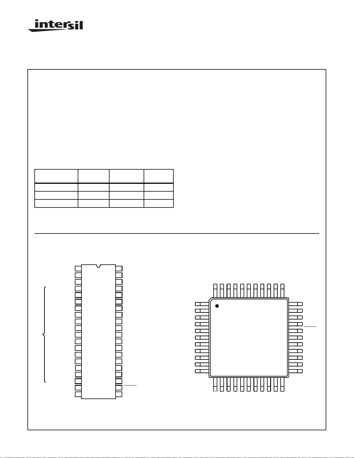
Ordering Information
TEMP.
PART NUMBER
RANGE (oC) PACKAGE PKG. NO.
ICL7129CPL 0 to 70 40 Ld PDIP E40.6
ICL7129RCPL 0 to 70 40 Ld PDIP E40.6
ICL7129CM44 0 to 70 44 Ld MQFP Q44.10x10
NOTE: “R” indicates device with reversed leads.
Pinouts
ICL7129 (PDIP)
TOP VIEW
Description
The Intersil ICL7129 is a very high performance 41/2-digit,
analog-to-digital converter that directly drives a multiplexed
liquid crystal display. This single chip CMOS integrated circuit requires only a few passive components and a reference
to operate. It is ideal for high resolution hand-held digital
multimeter applications.
The performance of the ICL7129 has not been equaled
before in a single chip A/D converter. The successive integr ation technique used in the ICL7129 results in accuracy better
than 0.005% of full scale and resolution down to 10µV/count.
The ICL7129, drawing only 1mA from a 9V battery, is well
suited for battery powered instruments. Provision has been
made for the detection and indication of a “LOW/BATTERY”
condition. Autoranging instruments can be made with the
ICL7129 which provides overrange and underrange outputs
and 10:1 range changing input. The ICL7129 instantly checks
for continuity, giving both a visual indication and a logic level
output which can enable an external audible transducer. These
features and the high performance of the ICL7129 make it an
extremely versatile and accurate instrument-on-a-chip .
ICL7129 (MQFP)
TOP VIEW
OSC2
1
OSC1
2
ANNUNCIATOR
B2, C2, LO BAT
DISPLA Y OUTPUT LINES
CAUTION: These devices are sensitive to electrostatic discharge; follow proper IC Handling Procedures.
http://www.intersil.com or 407-727-9207
OSC3
DRIVE
B
, C1, CONT
1
A
, G1, D
1
F1, E1, DP
A
, G2, D
2
F2, E2, DP
B3, C3, MINUS
A
, G3, D
3
F3, E3, DP
B4, C4, BC
A4, D4, G
F4, E4, DP
BP3
BP2
BP1
V
DISP
DP4/OR
3
4
5
1
6
1
7
8
2
9
2
10
11
3
12
3
13
5
14
4
15
4
16
17
18
19
20
40
DP
39
1
DP
38
2
37
RANGE
36
DGND
35
REF LO
REF HI
34
IN HI
33
32
IN LO
31
BUFF
C
30
REF-
C
29
REF+
28
COMMON
27
CONTINUITY
26
INT OUT
25
INT IN
24
V+
23
V-
22
LATCH/HOLD
DP
21
3
/UR
B
| Copyright © Intersil Corporation 1999
DGND
RANGE
OSC 2
OSC 1
OSC 3
ANNUNCE
DRIVE
, C1, CONT
1
3-31
DP
DP
2
1
NC
NC
IN HI
IN LO
REF HI
REF LO
44 43 42 41 40
1
2
3
4
5
6
7
8
9
10
11
12 13 14 15 16 17
1
1
, DP
1
, E
1
F
, LO BA T
, C
B
2
, D
2
, G
2
2
A
2
, D
, G
A
1
1
+
-
REF
REF
BUFF
C
39 38 37 36 35 34
2
, DP
2
, MINUS
, E
3
2
F
, C
3
B
C
COMMON
3
, D
3
, DP
, G
, E
3
A
F
CONTINUITY
3
5
, BC
3
4
, C
3
4
B
File Number 3085.1
INT IN
INT OUT
33
32
31
30
29
28
27
26
25
24
23
2221201918
4
4
, G
4
, DP
4
, D
, E
4
4
A
F
V+
VNC
NC
LATCH/
HOLD
/UR
DP
3
DP4/OR
V
DISP
BP1
BP2
BP3
Page 2
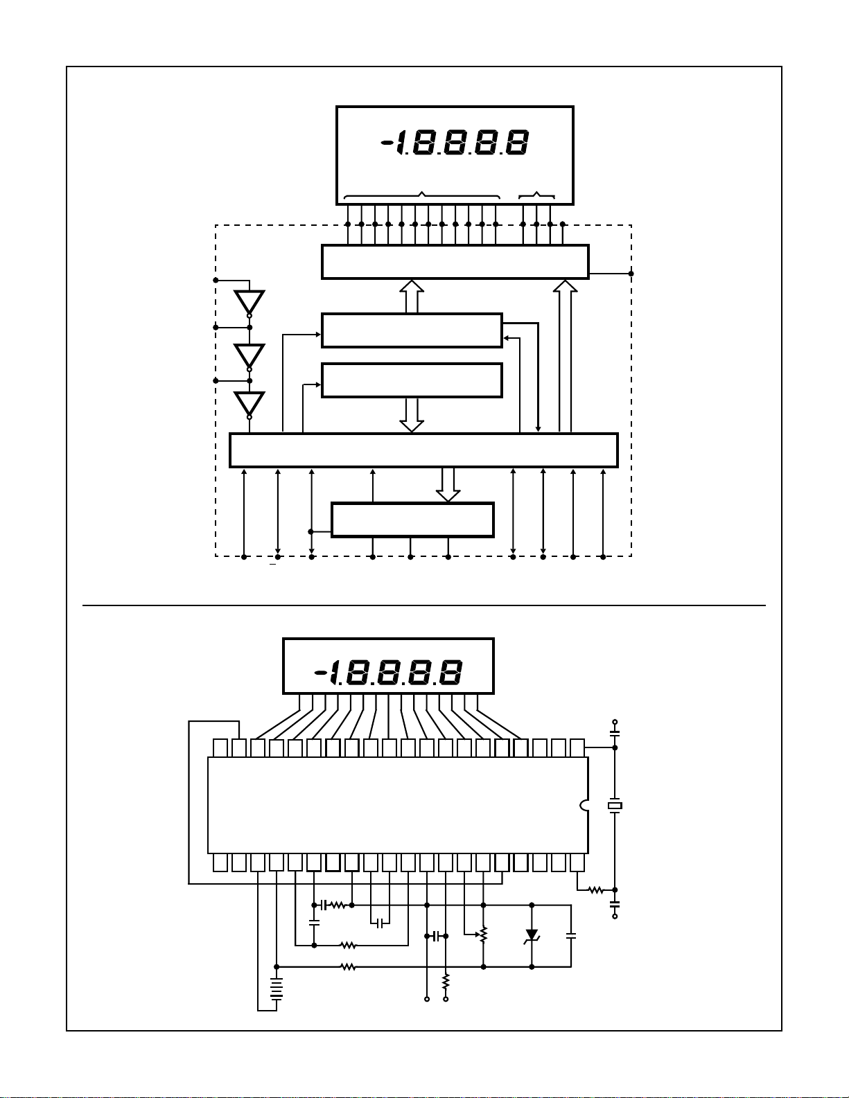
Functional Block Diagram
ICL7129
LOW BATTERY CONTINUITY
SEGMENT DRIVES
BACKPLANE
DRIVES
ANNUNCIATOR DRIVE
OSC1
OSC2
OSC3
Typical Application Schematic
LATCH, DECODE DISPLAY MULTIPLEXER
UP/DOWN RESULTS COUNTER
SEQUENCE COUNTER/DECODER
CONTROL LOGIC
ANALOG SECTION
DGNDV-V+CONTL/HRANGE
LOW BATTERY CONTINUITY
OR
DP
V
DISP
DP
DP
UR
DP
3
3
1
2
V+
5pF
13
14
15
16
17
18
19
20
10
11
12
7
8
9
4
5
6
1
2
3
ICL7129
28
27
26
25
24
23
22
21
31
30
29
34
33
32
37
36
35
40
39
38
(MICA)
120kHz
270K
560pF
(MICA)
1.2kΩ
150kΩ
10kΩ
+
1.0µF
20K
0.1µF
100kΩ
+
-
V
IN
ICL8069
6.8µF
0.1µF
+
9V
-
10pF
V+
3-32
Page 3
ICL7129
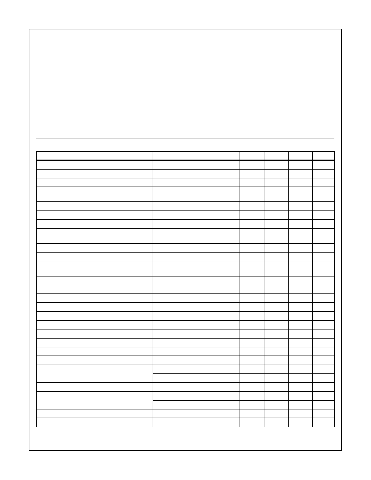
Absolute Maximum Ratings Thermal Information
Supply Voltage . . . . . . . . . . . . . . . . . . . . . . . . . . . . . . . . . . . . . . 15V
Reference Voltage (REF HI or REF LO). . . . . . . . . . . . . . . . V+ to V-
Input Voltage (Note 1), IN HI or IN LO . . . . . . . . . . . . . . . . . V+ to V-
V
. . . . . . . . . . . . . . . . . . . . . . . . . . . . . . . . . .DGND -0.3V to V+
DISP
Digital Input Pins
1, 2, 19, 20, 21, 22, 27, 37, 38, 39, 40 . . . . . . . . . . . . .DGND to V+
CAUTION: Stresses above those listed in “Absolute Maximum Ratings” may cause permanent damage to the device. This is a stress only rating and operation
of the device at these or any other conditions above those indicated in the operational sections of this specification is not implied.
NOTES:
1. Input voltages may exceed the supply voltages pro vided that input current is limited to 1400mA. Currents abo ve this value may result in
valid display readings but will not destroy the device if limited to ±1mA.
2. θJA is measured with the component mounted on an evaluation PC board in free air.
Thermal Resistance (Typical, Note 2) θJA (oC/W)
PDIP Package. . . . . . . . . . . . . . . . . . . . . . . . . . . . . . . 50
MQFP Package. . . . . . . . . . . . . . . . . . . . . . . . . . . . . . 80
Maximum Junction Temperature . . . . . . . . . . . . . . . . . . . . . 150oC
Maximum Storage Temperature Range . . . . . . . . . .-65oC to 150oC
Maximum Lead Temperature (Soldering 10s) . . . . . . . . . . . . . 300oC
(MQFP - Lead Tips Only)
Electrical Specifications V- to V+ = 9V, V
= 1.00V, TA = 25oC, f
REF
= 120kHz, Unless Otherwise Specified
CLK
PARAMETER TEST CONDITIONS MIN TYP MAX UNITS
Zero Input Reading VIN = 0V, 200mV Scale -0000 0000 +0000 Counts
Zero Reading Drift V
Ratiometric Reading V
Range Change Accuracy V
= 0V, 0oC To 70oC-±0.5 - µV/oC
IN
= V
IN
IN
= 1000mV, RANGE = 2V 9996 9999 10000 Counts
REF
= 0.10000V on Low,
0.9999 1.0000 1.0001 Ratio
Range ≈ VIN = 1.0000V on High Range
Rollover Error -V
= +VIN = 199mV - 1.5 3.0 Counts
IN
Linearity Error 200mV Scale - 1.0 - Counts
Input Common-Mode Rejection Ratio V
Input Common-Mode Voltage Range V
= 1V,VIN = 0V, 200mV Scale - 110 - dB
CM
= 0V, 200mV Scale - (V-) +1.5
IN
-V
(V+) -1.0
Noise (Peak-To-Peak V alue not Exceeded 95% of Time) V
Input Leakage Current V
Scale Factor Tempco V
= 0V 200mV Scale - 14 - µV
IN
= 0V, Pin 32, 33 - 1 10 pA
IN
= 199mV 0oC To 70oC
IN
External V
= 0ppm/oC
REF
- 2 7 ppm/oC
COMMON Voltage V+ to Pin 28 2.8 3.2 3.5 V
COMMON Sink Current ∆Common = + 0.1V - 0.6 - mA
COMMON Source Current ∆Common = -0.1V - 10 - µA
DGND VoItage V+ to Pin 36, V+ to V- = 9V 4.5 5.3 5.8 V
DGND Sink Current ∆DGND = +0.5V - 1.2 - mA
Supply Voltage Range V+ to V- (Note 3) 6 9 12 V
Supply Current Excluding COMMON Current V+ to V- = 9V - 1.0 1.5 mA
Clock Frequency (Note 3) - 120 360 kHz
V
Resistance V
DISP
to V+ - 50 - kΩ
DISP
Low Battery Flag Activation Voltage V+ to V- 6.3 7.2 7.7 V
CONTINUITY Comparator Threshold Voltages V
Pin 27 = HI 100 200 - mV
OUT
V
Pin 27 = LO - 200 400 mV
OUT
Pull-Down Current Pins 37, 38, 39 - 2 10 µA
“Weak Output” Current Sink/Source Pins 20, 21 Sink/Source - 3/3 - µA
Pin 27 Sink/Source - 3/9 - µA
Pin 22 Source Current -40-µA
Pin 22 Sink Current -3-µA
NOTE:
3. Device functionality is guaranteed at the stated Min/Max limits. However, accuracy can degrade under these conditions.
3-33
Page 4
Pin Descriptions
ICL7129
PIN SYMBOL DESCRIPTION
1 OSC
2 OSC
1
3
3 ANNUNCIATOR
DRIVE
4B
5A
6F
, C1, CONT Output to display segments.
1
, G1, D
1
, E1, DP
1
Input to first clock inverter.
Output of second clock inverter.
Backplane squarewave output for
driving annunciators.
Output to display segments.
1
Output to display segments.
1
7B2, C2, LO BATT Output to display segments.
8A
9F
, G2, D
2
, E2, DP
2
Output to display segments.
2
Output to display segments.
2
10 B3, C3, MINUS Output to display segments.
11 A3, G3, D
12 F3, E3, DP
13 B4, C4, BC
14 A4, D4, G
15 F4, E4, DP
16 BP
17 BP
18 BP
19 V
3
2
1
DlSP
Output to display segments.
3
Output to display segments.
3
Output to display segments.
5
Output to display segments.
4
Output to display segments.
4
Backplane #3 output to display.
Backplane #2 output to display.
Backplane #1 output to display.
Negative rail for display drivers.
20 DP4/OR INPUT: When HI, turns on most
significant decimal point.
OUTPUT: Pulled HI when result
count exceeds ±19,999.
21 DP3/UR INPUT: Second most significant
decimal point on when HI.
OUTPUT: Pulled HI when result
count is less than ±1,000.
22 LATCH/HOLD INPUT: When floating, A/D converter
operates in the free-run mode. When
pulled HI, the last displayed reading is
held. When pulled LO, the result
counter contents are shown
incrementing during the de-integrate
phase of cycle.
OUTPUT: Negative going edge
occurs when the data latches are
updated. Can be used for converter
status signal.
PIN SYMBOL DESCRIPTION
23 V- Negative power supply terminal.
24 V+ Positive power supply terminal, and
positive rail for display drivers.
25 INT IN Input to integrator amplifier.
26 INT OUT Output of integrator amplifier.
27 CONTINUITY INPUT: When LO, continuity flag on
the display is off. When HI,
continuity flag is on.
OUTPUT: HI when voltage between
inputs is less than +200mV. LO
when voltage between inputs is
more than +200mV.
28 COMMON Sets common-mode voltage of 3.2V
below V+ for DE, 10X, etc., Can be
used as pre-regulator for external
reference.
29 C
+ Positive side of external reference
REF
capacitor.
30 C
- Negative side of external reference
REF
capacitor.
31 BUFFER Output of buffer amplifier.
32 IN LO Negative input voltage terminal.
33 IN HI Positive input voltage terminal.
34 REF HI Positive reference voltage input
terminal.
35 REF LO Negative reference voltage input
terminal.
36 DGND Ground reference for digital section.
37 RANGE 3µA pull-down for 200mV scale.
Pulled HIGH externally for 2V scale.
38 DP
2
Internal 3µA pull-down. When HI,
decimal point 2 will be on.
39 DP
1
Internal 3µA pull-down. When HI,
decimal point 1 will be on.
40 OSC2 Output of first clock inverter. Input of
second clock inverter.
3-34
Page 5

ICL7129
Detailed Description
The ICL7129 is a uniquely designed single chip A/D converter.
It features a new “successive integration” technique to achieve
10µV resolution on a 200mV full-scale range. To achieve this
resolution a 10:1 improvement in noise performance over
previous monolithic CMOS A/D converters was accomplished.
Previous integrating converters used an external capacitor to
store an offset correction voltage. This technique worked well
but greatly increased the equivalent noise bandwidth of the
converter. The ICL7129 removes this source of error (noise) by
not using an auto-zero capacitor. Offsets are cancelled using
digital techniques instead. Savings in external parts cost are
realized as well as improved noise perf ormance and elimination
of a source of electromagnetic and electrostatic pick-up.
In the overall Functional Block Diagram of the ICL7129 the
heart of this A/D converter is the sequence counter/decoder
which drives the control logic and keeps track of the many
separate phases required for each conversion cycle. The
sequence counter is constantly running and is a separate
counter from the up/down results counter which is activated
only when the integrator is de-integrating. At the end of a conversion the data remaining in the results counter is latched,
decoded and multiplexed to the liquid crystal display.
The analog section block diagram shown in Figure 1
includes all of the analog switches used to configure the voltage sources and amplifiers in the different phases of the
cycle. The input and reference switching schemes are very
similar to those in other less accurate integrating A/D converters. There are 5 basic configurations used in the full conversion cycle. Figure 2 illustrates a typical waveform on the
integrator output. INT, INT
, and INT2 all refer to the signal
1
integrate phase where the input voltage is applied to the
integrator amplifier via the buffer amplifier. In this phase, the
integrator ramps over a fixed period of time in a direction
opposite to the polarity of the input voltage.
DE
, DE2, and DE3 are the de-integrate phases where the
1
reference capacitor is switched in series with the buffer amplifier and the integrator ramps back down to the level it started
from before integrating. However, since the de-integrate phase
can terminate only at a clock pulse transition, there is always a
small overshoot of the integrator past the starting point. The
ICL7129 amplifies this overshoot by 10 and DE
larly DE
’s overshoot is amplified by 10 and DE3begins. At the
2
end of DE3the results counter holds a number with 5
of resolution. This was obtained by feeding counts into the
results counter at the 3
1
/2 digit level during DE1, into the 41/
begins. Simi-
2
1
/2 digits
digit level during DE2and the 51/2 digit level for DE3. The
effects of offset in the buffer, integrator, and comparator can
now be cancelled by repeating this entire sequence with the
inputs shorted and subtracting the results from the original
reading. For this phase INT
switch is closed to give the same
2
common-mode voltage as the measurement cycle. This
assures excellent CMRR. At the end of the cycle the data in the
up/down results counter is accurate to 0.02% of full scale and is
sent to the display driver for decoding and m ultiple xing.
2
C
INT
INT, IN INT OUT
X10
-
+
INTEGRATOR
REST X10 DE2REST X10 DE
INTEGRATOR
RESIDUE
VOLTAGE
10
100
1000 CLOCKS
COMPARATOR 1
+
-
COMPARATOR 2
3
+
-
TO DIGITAL
SECTION
BUFFER
2
DE
1
2000
CLOCKS
R
INT
C
REF
REF HI REF LO
DE DE
INT
IN HI
COMMON
IN LO
ZERO-INTEGRATE
FIGURE 2. INTEGRAT OR WAVEFORM FOR NEGA TIVE INPUT VOLT AGE SHOWING SUCCESSIVE INTEGRATION PHASES AND
RESIDUE VOLTAGE
1
DE- DE+
DE+
INT1, INT
AND
2
LATCH
NOTE: Shaded area greatly expanded
in time and amplitude.
DE-
INT
INT
INTEGRATE
1000 CLOCKS
10,000 CLOCKS
-
+
BUFFER
Z1, X10
REST, INT
FIGURE 1. ANALOG BLOCK DIAGRAM
1
DE-INTEGRATE ZERO-INTEGRATE
3-35
Page 6

ICL7129
COMMON, DGND, and “Low Battery”
The COMMON and DGND (Digital GrouND) outputs of the
ICL7129 are generated from internal zener diodes
(Figure 3). COMMON is included primarily to set the common-mode voltage for battery operation or for any system
where the input signals float with respect to the power supplies. It also functions as a pre-regulator for an external precision reference voltage source. The v oltage betw een DGND
and V+ is the supply voltage for the logic section of the
ICL7129 including the display multiplexer and drivers. Both
COMMON and DGND are capable of sinking current from
external loads, but caution should be taken to ensure that
these outputs are not overloaded. Figure 4 shows the connection of external logic circuitry to the ICL7129. This connection will work providing that the supply current
requirements of the logic do not exceed the current sink
capability of the DGND pin. If more supply current is
required, the buffer in Figure 5 can be used to keep the loading on DGND to a minimum. COMMON can source approximately 12mA while DGND has no source capability.
24
V+
3.2V
28
COMMON
-
N
+
“LOW
BATTERY”
N
FIGURE 3. BIASING STRUCTURE FOR COMMON AND DGND
LOGIC
SECTION
5V
36
P
DGND
23
V-
V+
24
EXTERNAL
LOGIC
EXTERNAL
LOGIC
CURRENT
-
+
FIGURE 5. BUFFERED DGND
ICL7129
36
DGND
23
V-
The “LOW BATTERY” annunciator of the display is turned on
when the voltage between V+ and V- drops below 7.2V typically. The exact point at which this occurs is determined by
the 6.3V zener diode and the threshold voltage of the
N-Channel transistor connected to the V- rail in Figure 3. As
the supply voltage decreases, the N-Channel transistor
connected to the V-rail eventually turns off and the “LOW
BATTERY” input to the logic section is pulled HIGH, turning
on the “LOW BATTERY” annunciator.
I/O Ports
Four pins of the ICL7129 can be used as either inputs or outputs. The specific pin numbers and functions are described
in the Pin Description table. If the output function of the pin is
not desired in an application it can easily be overridden by
connecting the pin to V+ (HI) or DGND (LO). This connection
will not damage the device because the output impedance of
these pins is quite high. A simplified schematic of these
input/output pins is shown in Figure 6. Since there is approximately 500kΩ in series with the output driver, the pin (when
used as an output) can only drive very light loads such as
4000 series, 74CXX type CMOS logic, or other high input
impedance devices. The output drive capability of these four
pins is limited to 3µA, nominally, and the input switching
threshold is typically DGND + 2V.
V+
24
EXTERNAL
LOGIC
ICL7129
36
DGND
I
LOGIC
23
V-
FIGURE 4. DGND SINK CURRENT
≈500kΩ
DP4/OR PIN 20
DP3/UR PIN 21
LATCH/HOLD PIN 22
CONTINUITY PIN 27
FIGURE 6. “WEAK OUTPUT”
ICL7129
LATCH/HOLD, Overrange, and Underrange Timing
LATCH/HOLD output (pin 22) will be pulled low during
The
the last 100 clock cycles of each full conversion cycle. During this time the final data from the ICL7129 counter is
latched and transferred to the display decoder and multiplexer. The conversion cycle and
LATCH/HOLD timing are
directly related to the clock frequency. A full conversion cycle
takes 30,000 clock cycles which is equivalent to 60,000
oscillator cycles. OverRange (OR pin 20) and UnderRange
3-36
Page 7

ICL7129
(UR pin 21) outputs are latched on the falling edge of
LATCH/HOLD and remain in that state until the end of the
next conversion cycle. In addition, digits 1 through 4 are
blanked during overrange. All three of these pins are “weak
outputs” and can be overridden with external drivers or pullup resistors to enable their input functions as described in
the Pin Description table.
Instant Continuity
A comparator with a built-in 200mV offset is connected
directly between INPUT HI and INPUT LO of the ICL7129
(Figure 7). The CONTINUITY output (pin 27) will be pulled
high whenever the voltage between the analog inputs is less
than 200mV. This will also turn on the “CONTINUITY”
annunciator on the display. The CONTINUITY output may be
used to enable an external alarm or buzzer, thereby giving
the ICL7129 an audible continuity checking capability.
-
IN HI
COMMON
IN LO
200mV
-
+
V
CONTINUITY
FIGURE 7. “INSTANT CONTINUITY” COMPARATOR AND
OUTPUT STRUCTURE
500kΩ
-
+
+
BUFFER
TO DISPLAY
DRIVER
(NOT LATCHED)
Since the CONTINUITY output is one of the four “weak outputs” of the ICL7129, the “continuity” annunciator on the display can be driven by an external source if desired. The
continuity function can be overridden with a pull-down resistor
connected between CONTINUITY pin and DGND (pin 36).
Display Configuration
The ICL7129 is designed to drive a triplexed liquid crystal
display. This type of display has three backplanes and is driven
in a multiplexed format similar to the ICM7231 display driver
family. The specific display format is shown in Figure 8. Notice
that the polarity sign, decimal points, “LOW BATTERY”, and
“CONTINUITY” annunciators are directly driven by the
ICL7129. The individual segments and annunciators are
addressed in a manner similar to row-column addressing. Each
backplane (row) is connected to one-third of the total number of
segments. BP1 has all F, A, and B segments of the four least
significant digits. BP2 has all of the C, E, and G segments. BP3
has all D segments, decimal points, and annunciators. The segment lines (columns) are connected in groups of three bringing
all segments of the display out on just 12 lines.
Annunciator Drive
A special display driver output is provided on the ICL7129
which is intended to drive various kinds of annunciators on
custom multiplexed liquid crystal displays . The ANNUNClATOR
DRIVE output (pin 3) is a squarewave signal running at the
backplane frequency, approximately 100Hz. This signal
swings from V
to V+ and is in sync with the three back-
DISP
plane outputs BP1, BP2, and BP3. Figure 9 shows these
four outputs on the same time and voltage scales.
Any annunciator associated with any of the three backplanes
can be turned on simply by connecting it to the ANNUNClATOR DRIVE pin. To turn an annunciator off connect if to its
backplane. An example of a display and annunciator drive
scheme is shown in Figure 10.
F4, E4, DP4
A4, G4, D4
B4, C4, BC5
F3, E3, DP3
A3, G3, D3
B3, C3, MINUS
LOW BATTERY CONTINUITY
f
c
e
a
f
b
g
e
c
d
a
f
b
g
e
c
d
a
f
b
g
e
c
d
a
f
b
BP1
BP2
BP3
BACKPLANE
CONNECTIONS
g
e
c
d
LOW BATTERY CONTINUITY
f
c
e
FIGURE 8. TRIPLEXED LIQUID CRYSTAL DISPLAY LAYOUT FOR ICL7129
a
f
b
g
e
c
d
a
f
b
g
e
c
d
a
f
b
g
e
c
d
a
f
b
g
e
c
d
B1, C1, CONTINUITY
A1, G1, D1
F1, E1, DP1
B2, C2, LOW BATTERY
A2, G2, D2
F2, E2, DP2
3-37
Page 8

ICL7129
BP1
BP2
BP3
ON SEG.
FIGURE 9. TYPICAL BACKPLANE AND ANNUNCIATOR
DRIVE WAVEFORM
ANNUNCIATOR
µ
m
K
AMPS
VOLTS
M
Ω
BACKPLANE
ANNUNCIATOR
BACKPLANE
LOW BATTERY CONTINUITY
FIGURE 10. MULTIMETER EXAMPLE SHOWING USE OF
ANNUNCIATOR DRIVE OUTPUT
Display Temperature Compensation
For most applications an adequate display can be obtained b y
connecting V
(pin 19) to DGND (pin 36). In applications
DlSP
where a wide temperature range is encountered, the voltage
drive levels for some triplexed liquid crystal displays ma y need
to vary with temperature in order to maintain good display
contrast and viewing angle. The amount of temperature
compensation will depend upon the type of liquid crystal used.
Display manufacturers can supply the temperature compensation requirements for their displays. Figure 11 shows two
circuits that can be adjusted to give a temperature compensation of ≈ +10mV/
between DGND and V
o
C between V+ and V
should have a low turn-on voltage
DISP
. The diode
DISP
to assure that no forward current is injected into the chip if
V
is more negative than DGND.
DISP
Component Selection
There are only three passive components around the
ICL7129 that need special consideration in selection. They
are the reference capacitor , integr ator resistor, and integrator
capacitor. There is no auto-zero capacitor like that found in
earlier integrating A/D converter designs.
The integrating resistor is selected to be high enough to
assure good current Iinearity from the buffer amplifier and
integrator and low enough that PC board leakage is not a
problem. A value of 150kΩ should be optimum for most applications. The integrator capacitor is selected to give an optimum integrator swing at full-scale. A large integ rator s wing will
reduce the effect of noise sources in the comparator but will
affect rollover error if the swing gets too close to the positive
rail (≈0.7V). This gives an optimum swing of ≈2.5V at fullscale. For a 150kΩ integrating resistor and 2 conversions per
second the value is 0.1µF. For different conversion rates, the
value will change in inverse proportion. A second requirement
for good linearity is that the capacitor have low dielectric
absorption. Polypropylene caps give good performance at a
reasonable price. Finally the foil side of the cap should be
connected to the integrator output to shield against pickup.
The only requirement for the reference cap is that it be low
leakage. In order to reduce the effects of stray capacitance,
a 1µF value is recommended.
Clock Oscillator
The ICL7129 achieves its digital range changing by integrating the input signal for 1000 clock pulses (2,000 oscillator
cycles) on the 2V scale and 10,000 clock pulses on the
200mV scale. To achieve complete rejection of 60Hz on both
scales, an oscillator frequency of 120kHz is required, giving
two conversions per second.
V+
1N4148
5K
75K
FIGURE 11. TWO METHODS FOR TEMPERATURE COMPENSATING THE LIQUID CRYSTAL DISPLAY
39K
-
+
200K
ICL7611
24
19
V
DISP
ICL7129
36
DGND
23
V-
20K
39K
2N2222
19
36
18K
V
DISP
ICL7129
DGND
V+
24
23
V-
3-38
Page 9

Y
ICL7129
In low resolution applications, where the converter uses only
1
/2 digits and 100µV resolution, an R-C type oscillator is ade-
3
quate. In this application a C of 51pF is recommended and the
resistor value selected from f
the converter is used to its full potential (4
= 0.45/RC. However, when
OSC
1
/2 digits and 10µV
resolution) a crystal oscillator is recommended to prevent the
noise from increasing as the input signal is increased due to
frequency jitter of the R-C oscillator. Both R-C and crystal oscillator circuits are shown in Figure 12.
ICL7129
240
ICL7129
240
CRYSTAL MODE:
PARALLEL
R
V-
C
C
< 50kΩ
S
< 12pF
L
< 5pF
O
V+
1
75kΩ
1
27kΩ
120kHz5pF
51pF
10pF
FIGURE 12. RC AND CRYSTAL OSCILLATOR CIRCUITS
Powering the ICL7129
The ICL7129 may be operated as a battery powered hand-held
instrument or integrated into larger systems that have more
sophisticated power supplies. Figures 13, 14, and 15 show
various powering modes that may be used with the ICL7129.
The standard supply connection using a 9V battery is shown
in the Typical Application Schematic.
The power connection for systems with +5V and -5V supplies available is shown in Figure 13. Notice that measurements are with respect to ground. COMMON is also tied to
INLO to remove any common-mode voltage swing on the
integrator amplifier inputs.
+5V
24
V+
0.1µF
0.1µF
0.1µF
-5V
36
REF HI
REF LO
ICL7129
DGND
V-
FIGURE 13. POWERING THE ICL7129 FROM +5V AND -5V
COM
IN HI
IN LO
23
34
35
28
33
32
ICL8089
V
IN
It is important to notice that in Figure 13, digital ground of the
ICL7129 (DGND pin 36) is not directly connected to power
supply ground. DGND is set internally to approximately 5V
less than the V+ terminal and is not intended to be used as a
power input pin. It may be used as the ground reference for
external logic, as shown in Figure 4 and 5. In Figure 4, DGND
is used as the negative supply rail for external logic provided
that the supply current for the external logic does not cause
excessive loading on DGND. The DGND output can be buffered as shown in Figure 5. Here, the logic supply current is
shunted away from the ICL7129 keeping the load on DGND
low . This treatment of the DGND output is necessary to insure
compatibility when the external logic is used to interface
directly with the logic inputs and outputs of the ICL7129.
When a battery voltage between 3.8V and 6V is desired for
operation, a voltage doubling circuit should be used to bring
the voltage on the ICL7129 up to a lev el within the po w er supply voltage range. This operating mode is shown in Figure 14.
24
+
-
3.8V TO
6V
3
ICL7660
V+
REF HI
REF LO
ICL7129
36
DGND
8
2
+
4
10µF
5
10µF
+
V-
COM
IN HI
IN LO
23
34
35
28
33
32
+
V
IN
-
FIGURE 14. POWERING THE ICL7129 FROM A 3.8V T O 6V B ATTER
Again measurements are made with respect to COMMON
since the entire system is floating. Voltage doubling is
accomplished by using an ICL7660 CMOS voltage converter
and two inexpensive electrolytic capacitors . The same principle applies in Figure 15 where the ICL7129 is being used in
a system with only a single +5V power supply. Here measurements are made with respect to power supply ground.
+5V
24
V+
0.1µF
3
8
ICL7660
2
4
5
0.1µF
+
10µF
+
36
10µF
ICL7129
V-
FIGURE 15. POWERING THE ICL7129 FROM A SINGLE
POLARITY POWER SUPPLY
34
35
28
33
32
23
ICL8089
V
IN
+
-
3-39
Page 10

ICL7129
A single polarity power supply can be used to power the
ICL7129 in applications where battery operation is not
appropriate or convenient only if the power supply is isolated
from system ground. Measurements must be made with
respect to COMMON or some other voltage within its input
common-mode range.
Voltage References
The COMMON output of the ICL7129 has a temperature
coefficient of ±80ppm/
o
C typically. This voltage is only suitable as a reference voltage for applications where ambient
temperature variations are expected to be minimal. When
the ICL7129 is used in most environments, other voltage references should be considered. The diagram in the Typical
Application Schematic and Figure 15 show the ICL8069
1.2V band-gap voltage source used as the reference for the
ICL7129, and the COMMON output as its pre-regulator. The
reference voltage for the ICL7129 is set to 1.000V for both
2V and 200mV full-scale operation.
Multiple Integration A/D Converter
Equations
Oscillator Frequency
= 0.45/RC
f
OSC
C
> 50pF; R
OSC
f
(Typ) = 120kHz
OSC
or
f
= 120kHz Crystal (Recommended)
OSC
Oscillator Period
= 1/f
t
OSC
OSC
Integration Clock Period
CLOCK
= 2*t
OSC
t
Integration Period
t
t
= 1000*t
INT(2V)
INT(200mV)
= 10,000*t
60/50Hz Rejection Criterion
t
INT/t60Hz
or t
Optimum Integration Current
= 13µA
I
INT
Full Scale Analog Input Voltage
(Typ) = 200mV or 2V
V
INFS
ZERO-INTEGRATE
> 50kΩ
OSC
CLOCK
INT/t50Hz
LATCH
AND
CLOCK
= Integer
(Range = 1)
(Range = 0)
INT
1
INTEGRATE
DE
1
DE-INTEGRATE ZERO-INTEGRATE
Integrate Resistor
= V
R
INT
R
INFS/IINT
(Typ) = 150kΩ
INT
Integrate Capacitor
t
()I
()
INT
C
INT
INT
----------------------------------=
V
INT
Integrator Output Voltage Swing
t
()I
()
INT
V
INT
V
Maximum Swing: (V- + 0.5V) < V
INT
INT
----------------------------------=
C
INT
Display Count
V
IN
COUNT 10 000
(2V Range)
COUNT 10 000
(200mV Range)
Minimum V
REF
× Range =1(),=
× Range = 0(),=
: 500mV
---------------- -
V
REF
VIN10×
-----------------------
V
REF
Common Mode Input Voltage
(V- + 1V) < V
Auto Zero Capacitor: C
< (V+ - 0.5V)
IN
not used
AZ
Reference Capacitor: 0.1µF < C
V
COM
Biased Between V+ and V-.
V
≅ V+ -2.9V
COM
Regulation lost when V+ to V- < ≅6.4V.
If V
V
is externally pulled down to (V+ to V-)/2, the
COM
circuit will turn off.
COM
Power Supply: Single 9V
V+ - V- = 9V
Digital supply is generated internally
≅ V+ - 4.5V
V
GND
Display: Triplexed LCD
Continuity Output On if
V
INHI
to V
INLO
< 200mV
Conversion Cycle (In Both Ranges)
= t
t
CYC
REST X10 DE2REST X10 DE
CLOCK
x 30,000
3
REF
< 1µF
< (V+ - 0.7V)
INT
NOTE: Shaded area greatly expanded
in time and amplitude.
1000 CLOCKS
10,000 CLOCKS
CLOCKS
2000
3-40
INTEGRATOR
RESIDUE
VOLTAGE
1000 CLOCKS
Page 11

ICL7129
All Intersil semiconductor products are manufactured, assembled and tested under ISO9000 quality systems certification.
Intersil products are sold by description only. Intersil Corporation reserves the right to make changes in circuit design and/or specifications at any time without
notice. Accordingly, the reader is cautioned to verify that data sheets are current before placing orders. Information furnished by Intersil is believed to be accurate
and reliable. However, no responsibility is assumed by Intersil or its subsidiaries for its use; nor for any infringements of patents or other rights of third parties which
may result from its use. No license is granted by implication or otherwise under an y patent or patent rights of Intersil or its subsidiaries.
For information regarding Intersil Corporation and its products, see web site http://www.intersil.com
Sales Office Headquarters
NORTH AMERICA
Intersil Corporation
P. O. Box 883, Mail Stop 53-204
Melbourne, FL 32902
TEL: (407) 724-7000
FAX: (407) 724-7240
EUROPE
Intersil SA
Mercure Center
100, Rue de la Fusee
1130 Brussels, Belgium
TEL: (32) 2.724.2111
FAX: (32) 2.724.22.05
3-41
ASIA
Intersil (Taiwan) Ltd.
Taiwan Limited
7F-6, No. 101 Fu Hsing North Road
Taipei, Taiwan
Republic of China
TEL: (886) 2 2716 9310
FAX: (886) 2 2715 3029
 Loading...