

Page 1
ICL232
August 1997
+5V Powered, Dual RS-232 Transmitter/Receiver
Features
• Meets All RS-232C and V.28 Specifications
• Requires Only Single +5V Power Supply
• Onboard Voltage Doubler/Inverter
• Low Power Consumption
• 2 Drivers
- ±9V Output Swing for +5V lnput
- 300Ω Power-off Source Impedance
- Output Current Limiting
- TTL/CMOS Compatible
- 30V/µs Maximum Slew Rate
• 2 Receivers
- ±30V Input Voltage Range
-3kΩ to 7kΩ Input Impedance
- 0.5V Hysteresis to Improve Noise Rejection
• All Critical Parameters are Guaranteed Over the Entire
Commercial, Industrial and Military Temperature Ranges
Applications
• Any System Requiring RS-232 Communications Port
- Computer - Portable and Mainframe
- Peripheral - Printers and Terminals
- Portable Instrumentation
- Modems
• Dataloggers
Description
The ICL232 is a dual RS-232 transmitter/receiver interface
circuit that meets all ElA RS-232C and V.28 specifications. It
requires a single +5V power supply, and features two
onboard charge pump voltage converters which generate
+10V and -10V supplies from the 5V supply.
The drivers feature true TTL/CMOS input compatibility, slewrate-limited output, and 300Ω power-off source impedance.
The receivers can handle up to +30V, and ha v e a 3kΩ to 7kΩ
input impedance. The receivers also have hysteresis to
improve noise rejection.
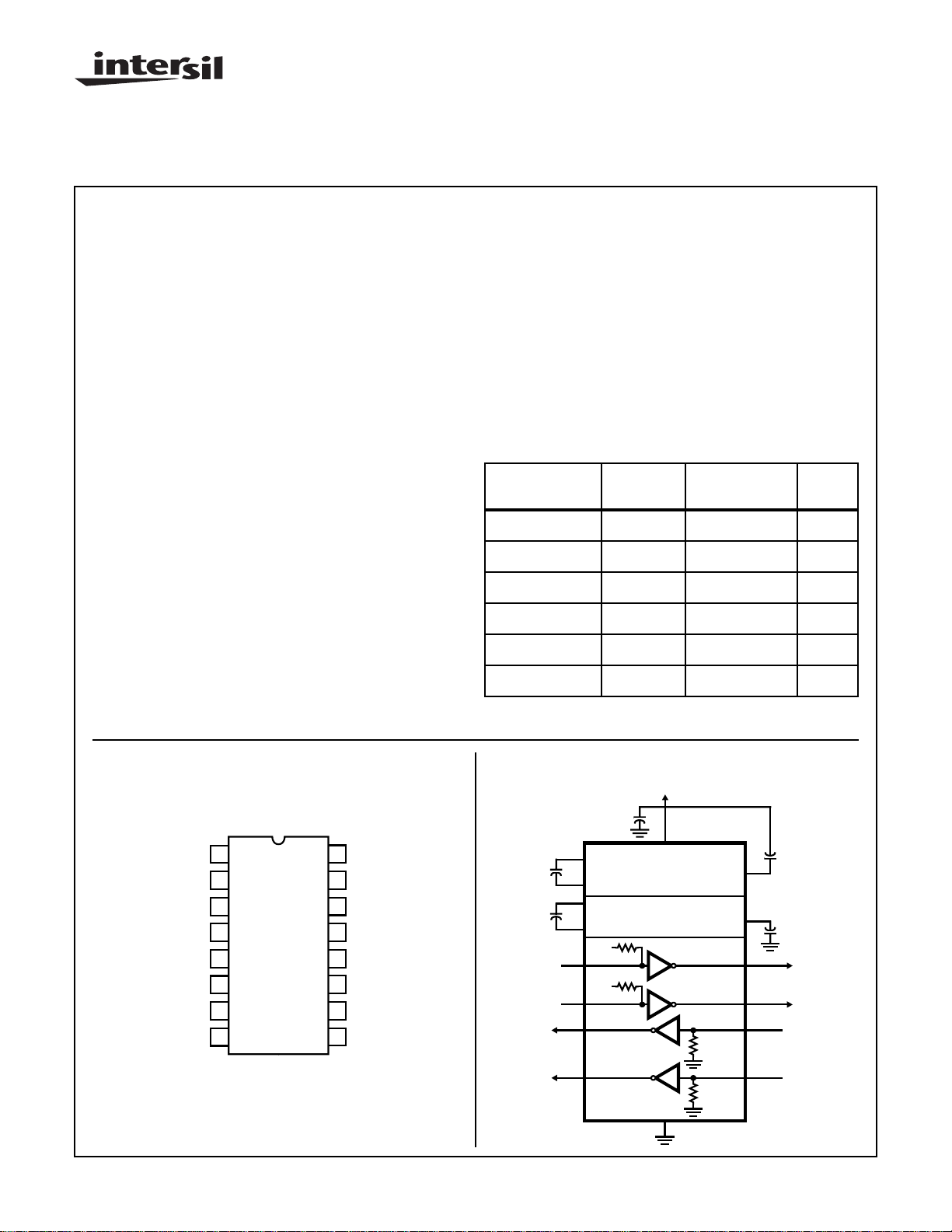
Ordering Information
TEMP.
PART NUMBER
RANGE (oC) PACKAGE
ICL232CPE 0 to 70 16 Ld PDIP E16.3
ICL232CBE 0 to 70 16 Ld SOIC M16.3
ICL232lPE -40 to 85 16 Ld PDIP E16.3
ICL232lJE -40 to 85 16 Ld CERDIP F16.3
ICL232lBE -40 to 85 16 Ld SOIC M16.3
ICL232MJE -55 to 125 16 Ld CERDIP F16.3
PKG.
NO.
Pinout
Functional Diagram
ICL232 (PDIP, CERDIP, SOIC)
TOP VIEW
C1+
1
V+
2
C1-
3
C2+
4
C2-
5
6
V-
T2
7
OUT
R2
8
IN
CAUTION: These devices are sensitive to electrostatic discharge; follow proper IC Handling Procedures.
http://www.intersil.com or 407-727-9207
| Copyright © Intersil Corporation 1999
16
V
CC
15
GND
14
T1
OUT
13
R1
IN
R1
12
OUT
T1
11
IN
T2
10
IN
9
R2
OUT
R1
R2
1µF
1µF
T1
T2
OUT
OUT
IN
IN
8-49
+5V
+
1.0µF
1
C1+
+
3
VOLTAGE INVERTER
C1-
4
C2+
+
5
VOLTAGE INVERTER
C2-
+5V
400kΩ
11
+5V
400kΩ
10
16
V
CC
+5V TO 10V
+10V TO -10V
T1
T2
R1
R2
15
5kΩ
5kΩ
V+
1µF
+
2
6
V-
1µF
+
14
7
1312
89
R1
R2
T1
T2
OUT
OUT
IN
IN
File Number 3020.5
Page 2
ICL232
Absolute Maximum Ratings Thermal Information
VCC to Ground . . . . . . . . . . . . . . . . . . . . . .(GND -0.3V) < VCC < 6V
V+ to Ground . . . . . . . . . . . . . . . . . . . . . . . (VCC -0.3V) < V+ < 12V
V- to Ground. . . . . . . . . . . . . . . . . . . . . . . -12V < V- < (GND +0.3V)
Input Voltages
T1IN, T2IN. . . . . . . . . . . . . . . . . . . . (V- -0.3V) < VIN < (V+ +0.3V)
R1IN, R2IN . . . . . . . . . . . . . . . . . . . . . . . . . . . . . . . . . . . . . . ±30V
Output Voltages
T1
, T2
R1
OUT
OUT
. . . . . . . . . . . . (V- -0.3V) < V
OUT
, R2
. . . . . . . . .(GND -0.3V) < V
OUT
RXOUT
< (V+ +0.3V)
TXOUT
< (VCC +0.3V)
Short Circuit Duration
T1
, T2
. . . . . . . . . . . . . . . . . . . . . . . . . . . . . . Continuous
OUT
, R2
. . . . . . . . . . . . . . . . . . . . . . . . . . . . . . Continuous
OUT
R1
OUT
OUT
Operating Conditions
Temperature Ranges
ICL232C . . . . . . . . . . . . . . . . . . . . . . . . . . . . . . . . . . .0oC to 70oC
ICL232I . . . . . . . . . . . . . . . . . . . . . . . . . . . . . . . . . . -40oC to 85oC
ICL232M . . . . . . . . . . . . . . . . . . . . . . . . . . . . . . . . -55oC to 125oC
CAUTION: Stresses above those listed in “Absolute Maximum Ratings” may cause permanent damage to the device. This is a stress only rating and operation
of the device at these or any other conditions above those indicated in the operational sections of this specification is not implied.
NOTE:
1. θJA is measured with the component mounted on an evaluation PC board in free air.
Thermal Resistance (Typical, Note 1) θJA (oC/W) θJC (oC/W)
CERDIP Package . . . . . . . . . . . . . . . . 80 18
PDIP Package. . . . . . . . . . . . . . . . . . . 100 N/A
SOIC Package. . . . . . . . . . . . . . . . . . . 100 N/A
Maximum Junction Temperature
Plastic Packages. . . . . . . . . . . . . . . . . . . . . . . . . . . . . . . . . 150oC
Ceramic Package . . . . . . . . . . . . . . . . . . . . . . . . . . . . . . . . 175oC
Maximum Storage Temperature Range . . . . . . . . . .-65oC to 150oC
Maximum Lead Temperature (Soldering 10s). . . . . . . . . . . . . 300oC
Electrical Specifications Test Conditions: V
= +5V ±10%, TA = Operating Temperature Range. Test Circuit as in Figure 8
CC
Unless Otherwise Specified
PARAMETER TEST CONDITIONS MIN TYP MAX UNITS
Transmitter Output Voltage Swing, T
OUT
T1
OUT
and T2
Loaded with 3kΩ
OUT
±5 ±9 ±10 V
to Ground
Power Supply Current, I
TIN, Input Logic Low, V
TIN, Input Logic High, V
Logic Pullup Current, I
CC
lL
lH
P
RS-232 Input Voltage Range, V
Receiver Input Impedance, R
IN
IN
Outputs Unloaded, TA = 25oC-510mA
- - 0.8 V
2.0 - - V
T1IN, T2IN = 0V - 15 200 µA
-30 - +30 V
VIN = ±3V 3.0 5.0 7.0 kΩ
Receiver Input Low Threshold, VlN (H-L) VCC = 5V, TA = 25oC 0.8 1.2 - V
Receiver Input High Threshold, VIN (L-H) VCC = 5V, TA = 25oC - 1.7 2.4 V
Receiver Input Hysteresis, V
TTL/CMOS Receiver Output Voltage Low, VOLI
TTL/CMOS Receiver Output Voltage High, VOHI
Propagation Delay, t
PD
HYST
= 3.2mA - 0.1 0.4 V
OUT
= -1.0mA 3.5 4.6 - V
OUT
RS-232 to TTL - 0.5 - µs
Instantaneous Slew Rate, SR CL = 10pF, RL = 3kΩ, TA = 25oC
0.2 0.5 1.0 V
- - 30 V/µs
(Notes 2, 3)
Transition Region Slew Rate, SR
T
RL = 3kΩ, CL = 2500pF Measured
-3-V/µs
from +3V to -3V or -3V to +3V
Output Resistance, R
OUT
RS-232 Output Short Circuit Current, I
SC
VCC = V+ = V- = 0V, V
T1
OUT
or T2
Shorted to GND - ±10 - mA
OUT
= ±2V 300 - - Ω
OUT
NOTES:
2. Guaranteed by design.
3. See Figure 4 for definition.
8-50
Page 3

Test Circuits
ICL232
-
1µF
C3
+
1µF
C1
1µF
C2
1µF C4
3kΩ
T2 OUTPUT
RS-232
±30V INPUT
C1+
1
+
-
+
-
V+
2
C1-
3
C2+
4
C2-
5
-
+
V-
6
T2
7
OUT
8
R2
IN
T1
R1
R2
V
CC
GND
OUT
R1
OUT
T1
T2
OUT
IN
IN
IN
FIGURE 1. GENERAL TEST CIRCUIT FIGURE 2. POWER-OFF SOURCE RESISTANCE
Typical Performance Curves
550
500
TA = 25oC
450
EXTERNAL SUPPLY LOAD
400
1kΩ BETWEEN V+ + GND
OR V- + GND
350
TRANSMITTER OUTPUT
OPEN CIRCUIT
300
250
V+, V- SUPPLY IMPEDANCES (Ω)
200
150
3456
V+ SUPPLY
INPUT SUPPLY VOLTAGE VCC (V)
FIGURE 3. V+, V- OUTPUT IMPEDANCES vs V
GUARANTEED
OPERATING
RANGE
16
15
14
13
12
11
10
9
V- SUPPLY
+4.5V TO
+5.5V INPUT
3kΩ
T1 OUTPUT
RS-232
±30V INPUT
TTL/CMOS
OUTPUT
TTL/CMOS
INPUT
TTL/CMOS
INPUT
TTL/CMOS
OUTPUT
CC
C1+
1
V+
2
C1-
3
C2+
4
C2-
5
6
VT2
7
R2
8
R
OUT
VIN = ±2V
OUT
IN
= VIN/I
A
T1
R1
R2
V
CC
GND
OUT
R1
OUT
T1
T2
OUT
T2
T1
IN
IN
IN
16
15
14
13
12
11
10
9
OUT
OUT
CONFIGURATION
10
9
8
7
6
5
OUTPUT VOLTAGE (|V|)
4
3
V- (VCC = 4.5V)
TA = 25oC
TRANSMITTER OUTPUTS
OPEN CIRCUIT
V+ (VCC = 4.5V)
|I
| (mA)
LOAD
V+ (VCC = 5V)
V- (VCC = 5V)
9876543210
FIGURE 4. V+, V- OUTPUT VOLTAGES vs LOAD CURRENT
10
Pin Descriptions
PDIP, CERDIP SOIC PIN NAME DESCRIPTION
1 1 C1+ External capacitor “+” for internal voltage doubler.
2 2 V+ Internally generated +10V (typical) supply.
3 3 C1- External capacitor “-” for internal voltage doubler.
4 4 C2+ External capacitor “+” internal voltage inverter.
5 5 C2- External capacitor “-” internal voltage inverter.
6 6 V- Internally generated -10V (typical) supply.
77T2
88R2
OUT
IN
9 9 R2out Receiver 2 TTL/CMOS output.
10 10 T2
11 11 T1
IN
IN
RS-232 Transmitter 2 output ±10V (typical).
RS-232 Receiver 2 input, with internal 5K pulldown resistor to GND.
Transmitter 2 TTL/CMOS input, with internal 400K pullup resistor to VCC.
Transmitter 1 TTL/CMOS input, with internal 400K pullup resistor to VCC.
8-51
Page 4

ICL232
Pin Descriptions
(Continued)
PDIP, CERDIP SOIC PIN NAME DESCRIPTION
12 12 R1
13 13 R1
14 14 T1
OUT
IN
OUT
Receiver 1 TTL/CMOS output.
RS-232 Receiver 1 input, with internal 5K pulldown resistor to GND.
RS-232 Transmitter 1 output ±10V (typical).
15 15 GND Supply Ground.
16 16 V
VOLTAGE DOUBLER
V
CC
GND
RC
OSCILLATOR
S1
S3
C1
C1-
CC
+
S2
+
C1
-
S4
Positive Power Supply +5V ±10%
GND
CC
S5
S7
V+ = 2V
+
C3
-
V
CC
VOLTAGE INVERTER
FIGURE 5. DUAL CHARGE PUMP
Detailed Description
The ICL232 is a dual RS-232 transmitter/receiver powered by
a single +5V power supply which meets all ElA RS232C specifications and features low power consumption. The functional
diagram illustrates the major elements of the ICL232. The circuit is divided into three sections: a voltage doubler/inverter,
dual transmitters, and dual receivers Voltage Converter.
An equivalent circuit of the dual charge pump is illustrated in
Figure 5.
The voltage quadrupler contains two charge pumps which use
two phases of an internally generated clock to generate +10V
and -10V. The nominal clock frequency is 16kHz. During
phase one of the clock, capacitor C1 is charged to V
During phase two, the voltage on C1 is added to V
producing a signal across C2 equal to twice V
time, C3 is also charged to 2V
, and then during phase one,
CC
. At the same
CC
it is inverted with respect to ground to produce a signal across
C4 equal to -2V
. The voltage converter accepts input
CC
voltages up to 5.5V. The output impedance of the doub ler (V+)
is approximately 200Ω, and the output impedance of the
inverter (V-) is approximately 450Ω. Typical graphs are
presented which show the voltage converters output vs input
voltage and output voltages vs load characteristics. The test
circuit (Figure 3) uses 1µF capacitors for C1-C4, however, the
value is not critical. Increasing the values of C1 and C2 will
lower the output impedance of the voltage doubler and
inverter, and increasing the values of the reservoir capacitors,
C3 and C4, lowers the ripple on the V+ and V- supplies.
T1IN, T2
IN
T1
, T2
OUT
OUT
Instantaneous
Slew Rate (SR)
FIGURE 6. SLEW RATE DEFINITION
90%
10%
t
f
(0.8) (VOH - VOL)
=
t
r
t
r
(0.8) (VOL - VOH)
or
V
OH
V
OL
t
f
Transmitters
The transmitters are TTL/CMOS compatible inverters which
translate the inputs to RS-232 outputs. The input logic threshold is about 26% of V
the input results in a voltage of between -5V and V- at the output, and a logic 0 results in a voltage between +5V and (V+
- 0.6V). Each transmitter input has an inter nal 400kΩ pullup
resistor so any unused input can be left unconnected and its
output remains in its low state. The output voltage swing
meets the RS-232C specification of ±5V minimum with the
worst case conditions of: both transmitters driving 3kΩ minimum load impedance, V
.
CC
operating temperature. The transmitters have an internally
,
CC
limited output slew rate which is less than 30V/µs. The outputs
are short circuit protected and can be shorted to ground indefinitely. The powered down output impedance is a minimum of
300Ω with ±2V applied to the outputs and V
V+
V
CC
T
XIN
GND < T
XIN
< V
CC
V-
FIGURE 7. TRANSMITTER
Receivers
The receiver inputs accept up to ±30V while presenting the
required 3kΩ to 7kΩ input impedance even it the pow er is off
(V
= 0V). The receivers have a typical input threshold of
CC
1.3V which is within the ±3V limits, known as the transition
region, of the RS-232 specification. The receiver output is
0V to V
. The output will be low whenever the input is
CC
greater than 2.4V and high whenever the input is floating or
driven between +0.8V and -30V. The receivers feature 0.5V
hysteresis to improve noise rejection.
+
C2
C2-
S6
+
C2
-
S8
, or 1.3V for VCC = 5V. A logic 1 at
CC
= 4.5V, and maximum allowable
CC
400kΩ
300Ω
+
C4
-
= 0V.
CC
V- < V
T
OUT
TOUT
GND
V- = -(V+)
< V+
8-52
Page 5

ICL232
V
CC
R
-30V < R
XIN
GND
XIN
< +30V
5kΩ
GND < V
R
OUT
ROUT
< V
CC
FIGURE 8. RECEIVER
T1IN, T2
IN
OR
, R2
R1
IN
IN
T1
, T2
OUT
OUT
OR
, R2
R1
OUT
OUT
t
PHL
Average Propagation Delay =
t
PLH
t
PHL +tPLH
2
V
OH
V
OL
FIGURE 9. PROPAGATION DELAY DEFINITION
Applications
The ICL232 may be used for all RS-232 data terminal and
communication links. It is particularly useful in applications
where ±12V power supplies are not available for conventional RS-232 interface circuits. The applications presented
represent typical interface configurations.
A simple duplex RS-232 port with CTS/RTS handshaking is
illustrated in Figure 10. Fixed output signals such as DTR
(data terminal ready) and DSRS (data signaling rate select)
is generated by driving them through a 5kΩ resistor
connected to V+.
+5V
16
1
+
C1
3
1µF
INPUTS
OUTPUTS
TTL/CMOS
C2
1µF
-
+
-
TD
RTS
RD
CTS
ICL232
4
5
T1
11
R2
T2
R1
10
12
9
FIGURE 10. SIMPLE DUPLEX RS-232 PORT WITH CTS/RTS
HANDSHAKING
C3
-
1µF
+
5kΩ
2
6
-
C4
1µF
+
14
TD (2) TRANSMIT DATA
7
RTS (4) REQUEST TO SEND
13
RD (3) RECEIVE DATA
8
CTS (5) CLEAR TO SEND
SIGNAL GROUND (7)15
CTR (20) DATA
TERMINAL READY
5kΩ
DSRS (24) DATA
SIGNALING RATE
SELECT
RS-232
INPUTS AND OUTPUTS
In applications requiring four RS-232 inputs and outputs
(Figure 11), note that each circuit requires two charge pump
capacitors (C1 and C2) but can share common reservoir
capacitors (C3 and C4). The benefit of sharing common reservoir capacitors is the elimination of two capacitors and the
reduction of the charge pump source impedance which
effectively increases the output swing of the transmitters.
INPUTS
OUTPUTS
TTL/CMOS
INPUTS
OUTPUTS
TTL/CMOS
C1
1µF
TD
RTS
RD
CTS
2µF
C1
1µF
DTR
DSRS
DCD
R1
1
+
-
C4
+
+
-
ICL232
3
T1
11
10
12
R2
9
-
V- V+
6
ICL232
1
3
T1
11
10
12
R2
9
R1
R1
4
+
C2
5
1µF
-
14
T2
T2
TD (2) TRANSMIT DAT A
7
RTS (4) REQUEST TO SEND
13
RD (3) RECEIVE DAT A
8
CTS (5) CLEAR TO SEND
15
26
C3
+
-
µF
2
2
16
4
+
C2
5
1µF
-
DTR (20) DAT A TERMINAL
14
READY
7
DSRS (24) DAT A SIGNALING
RATE SELECT
13
DCD (8) DAT A CARRIER
DETECT
8
R1 (22) RING INDICATOR
+5V
RS-232
INPUTS AND
OUTPUTS
SIGNAL GROUND (7)15
FIGURE 11. COMBINING TWO ICL232s FOR 4 PAIRS OF RS-232 INPUTS AND OUTPUTS
8-53
Page 6

ICL232
All Intersil semiconductor products are manufactured, assembled and tested under ISO9000 quality systems certification.
Intersil products are sold by description only. Intersil Corporation reserves the right to make changes in circuit design and/or specifications at any time without
notice. Accordingly, the reader is cautioned to verify that data sheets are current before placing orders. Information furnished by Intersil is believed to be accurate
and reliable. However, no responsibility is assumed by Intersil or its subsidiaries for its use; nor for any infringements of patents or other rights of third parties which
may result from its use. No license is granted by implication or otherwise under an y patent or patent rights of Intersil or its subsidiaries.
For information regarding Intersil Corporation and its products, see web site http://www.intersil.com
Sales Office Headquarters
NORTH AMERICA
Intersil Corporation
P. O. Box 883, Mail Stop 53-204
Melbourne, FL 32902
TEL: (407) 724-7000
FAX: (407) 724-7240
EUROPE
Intersil SA
Mercure Center
100, Rue de la Fusee
1130 Brussels, Belgium
TEL: (32) 2.724.2111
FAX: (32) 2.724.22.05
8-54
ASIA
Intersil (Taiwan) Ltd.
Taiwan Limited
7F-6, No. 101 Fu Hsing North Road
Taipei, Taiwan
Republic of China
TEL: (886) 2 2716 9310
FAX: (886) 2 2715 3029
 Loading...