Silicon Bipolar MMIC 5 GHz
Active Double Balanced
Mixer/IF Amp
Technical Data
IAM-81028
Features
• 8 dB RF-IF Conversion Gain
From 0.05 - 5 GHz
• IF Output from DC to 1 GHz
• Low Power Dissipation:
60 mW at V
• Single Polarity Bias Supply:
V
= 4 to 8 V
CC
•
Load-Insensitive Performance
• Conversion Gain Flat Over
Temperature
•
Low LO Power Requirements:
-5 dBm Typical
• Low RF to IF Feedthrough,
Low LO Leakage
• Hermetic Ceramic Surface
Mount Package
= 5 V Typ.
CC
Description
The IAM-81028 is a complete lowpower-consumption doublebalanced active mixer housed in a
miniature ceramic hermetic
surface mount package. It is
designed for narrow or wide
bandwidth commercial, industrial
and military applications having
RF inputs up to 5 GHz and IF
outputs from DC to 1 GHz.
Operation at RF and LO
frequencies less than 50 MHz can
be achieved using optional
external capacitors to ground.
The IAM-81028 is particularly well
suited for applications that
require load-insensitive conversion gain and good spurious signal
suppression with minimum LO
and bias power consumption.
Typical applications include
frequency down conversion,
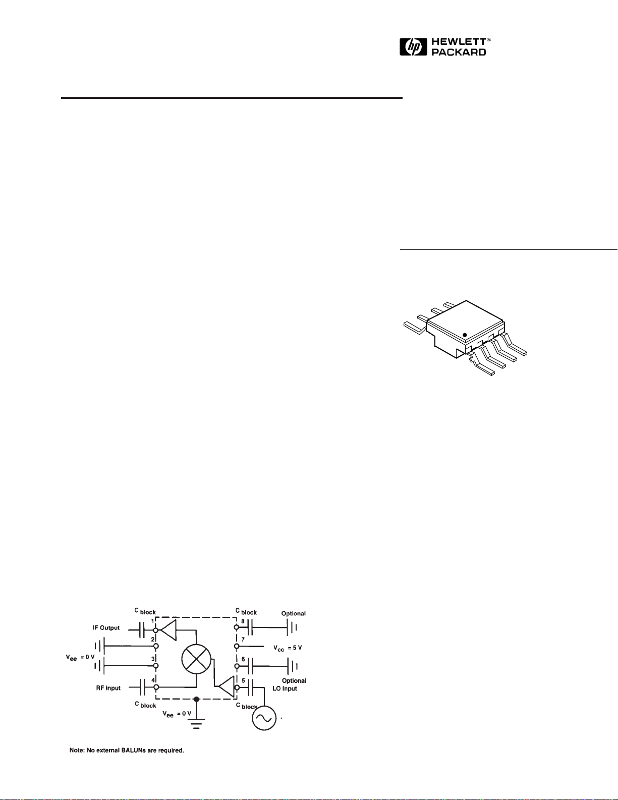
Typical Biasing Configuration and
Functional␣ Block␣ Diagram
28 Package
PIN 1
modulation, demodulation and
phase detection for fiber-optic,
GPS satellite navigation, mobile
radio, and battery powered
communications receivers.
The IAM series of Gilbert
multiplier-based frequency
converters is fabricated using
HP’s 10 GHz, fT, 25 GHz f
ISOSATTM-I silicon bipolar process. This process uses nitride self
alignment, submicrometer
lithography, trench isolation, ion
implantation, gold metallization
and polyimide inter-metal
dielectric and scratch protection
to achieve excellent performance,
uniformity and reliability.
MAX
7-123
5965-9108E

Absolute Maximum Ratings
Absolute
Parameter Maximum
Device Voltage 15 V
Power Dissipation
RF Input Power +14 dBm
LO Input Power +14 dBm
Junction Temperature 200°C
Storage Temperature -65°C to 200°C
[2,3]
300 mW
[1]
Thermal Resistance:
[2,4]
θjc = 50°C/W
Notes:
1. Permanent damage may occur if any of
these limits are exceeded.
2. T
= 25°C.
CASE
3. Derate at 20 mW/°C for TC > 185°C.
4. See MEASUREMENTS section “Thermal
Resistance” in Communications
Components Catalog, for more
information.
Electrical Specifications
T
= 25°C
A
[1]
Parameters and Test Conditions:
Symbol VCC = 5 V, Z
G
C
f
RF RF Bandwidth IF = 250 MHz GHz 4.5
3dB
Conversion Gain RF = 2 GHz, LO = 1.75 GHz dB 7.0 8.5 10
= 50 Ω , LO = -5 dBm, RF = -20 dBm Units Min. Typ. Max.
O
(GC 3 dB Down)
f
IF IF Bandwidth LO = 2 GHz GHz 0.6
3dB
(GC 3 dB Down)
P
1dB
IF Output Power at RF = 2 GHz, LO = 1.75 GHz dBm -6
1 dB Gain Compression
IP
3
IF Output Third Order RF = 2 GHz, LO = 1.75 GHz dBm 3
Intercept Point
NF SSB Noise Figure RF = 2 GHz, LO = 1.75 GHz dB 17
VSWR RF Port VSWR f = 0.05 to 5 GHz 1.5:1
LO Port VSWR f = 0.05 to 5 GHz 1.5:1
IF Port VSWR f < 1 GHz 1.5:1
RF
LO
LO
I
CC
Note:
1. The recommended operating voltage range for this device is 4 to 8 V. Typical performance as a function of voltage is on the following
page.
RF Feedthrough at IF Port RF = 2 GHz, LO = 1.75 GHz dBc -25
if
LO Leakage at IF Port LO = 1.75 GHz dBm -25
if
LO Leakage at RF Port LO = 1.75 GHz dBm -35
rf
Supply Current mA 10 12.5 16
7-124

Typical Performance, T
= 25° C, V
A
CC
= 5 V
RF: -20 dBm at 2 GHz, LO: -5 dBm at 1.75 GHz
(unless otherwise noted)
(dB)
C
G
10
5
0
15
10
(dB)
C
G
5
0
IF = 70 MHz
5
0
(dBm)
1 dB
IF P
–5
–10
02 46 810
G
Figure 1. Conversion Gain, IF P
and ICC Current vs. VCC Bias Voltage.
IF = 1 GHz
C
VCC (V)
I
CC
P
1 dB
1 dB
4:1
RF
LO
IF
3:1
VSWR
2:1
30
20
(mA)
CC
I
10
0
15
10
(dB)
C
G
5
0
5
0
G
(dBm)
1 dB
IF P
–5
–10
–55 –25 +25 +85 +125
C
P
1 dB
TEMPERATURE (°C)
I
CC
Figure 2. Conversion Gain, IF P
and ICC Current vs. Case Temperature.
10
8
6
(dB)
C
G
4
2
20
15
10
5
1 dB
(mA)
CC
I
–5
0.1 0.2 0.5 1.0 2.0 5.0 10
RF FREQUENCY (GHz)
Figure 3. Typical RF to IF Conversion
Gain vs. RF Frequency, TA = 25°C
(Low Side LO).
10
LO = 2 GHz
8
6
(dB)
C
4
G
2
0
–2
0.01 0.1 1.0 2.0
LO = 4 GHz
High Side LO
Low Side LO
FREQUENCY, RF–LO (GHz)
Figure 6. RF to IF Conversion Gain
vs. IF Frequency.
1:1
0.1 1.0 10
FREQUENCY (GHz)
Figure 4. RF, LO and IF Port VSWR
vs. Frequency.
0
RF to IF
LO to IF
LO to RF
–10
–20
RF to IF (dBc)
LO to RF and IF (dBm)
–30
–40
0.1 1.0 10
FREQUENCY (GHz)
Figure 7. RF Feedthrough Relative to
IF Carrier, dBm LO to RF and IF
Leakage vs. Frequency.
0
–15 –5 0–10 5
LO POWER (dBm)
Figure 5. RF to IF Conversion Gain
vs. LO Power.
—
21
35
>75
>75
>75
>75
>75
>75
>75
>75
>75
>75
>75
>75
>75
0
12
1
2
3
HARMONIC LO ORDER
4
5
0
13
41
36
28
27
49
45
35
48
48
39
71
53
57
49
72
63
62
012345
HARMONIC RF ORDER
Xmn = Pif – P(m*rf – n*lo)
Figure 8. Harmonic Intermodulation
Suppression (dB Below Desired Output)
RF at 1 GHz, LO at 0.752 GHz, IF at 0.248 GHz.
7-125

Package Dimensions
28 Package
1
2
3
4
8
1.27 (0.050) TYP.
7
6
5
TOP VIEW
4.57 ± 0.13
(0.180 ± 0.005 SQ)
5.33 ± 0.25
(0.210 ± 0.010)
8° MAX.
END VIEW
0.13 ± 0.05
(0.005 ± 0.002)
2.54 ± 0.25
(0.100 ± 0.010)
10.16 ± 0.25
(0.400 ± 0.010)
DIMENSIONS ARE IN MILLIMETERS (INCHES)
Package marking code is “M810”
0.38 ± 0.08
(0.015 ± 0.003)
0.76 ± 0.13
(0.030 ± 0.005)
0.08 ± 0.08
(0.003 ± 0.003)
(0.070 ± 0.010)
1.78 ± 0.25
2.08 ± 0.25
(0.082 ± 0.010)
SIDE VIEW
7-126
 Loading...