

Datasheet IA82050-PDW28C-01, IA82050-PDW28I-01, IA82050-PLC28C-01, IA82050-PLC28I-01 Datasheet (INOVC)
Page 1
IA82050 Data Sheet
ASYNCHRONOUS SERIAL CONTROLLER As of Production Ver. 01
FEATURES
• Form, Fit, and Function Compatible with the Intel 82050 and 82510
• Packaging options available: 28 Pin Plastic DIP and 28 Lead Plastic Leaded
Chip Carrier
• Asynchronous Serial Channel Operation
• Separate Transmit and Receive FIFOs with Programmable Threshold
• Programmable Baud Rate Generators up to 288K Baud
• Special Protocol Features
- Control Character Recognition
- Auto Echo and Loopback Modes
- 9-Bit Protocol Support
- 5 to 9 Bit Character Format
The IA82050 is a "plug-and-play" drop-in repla cement for the original IC. innovASIC produces replacement ICs
using its MILESTM, or Managed IC Lifetime Extension System, cloning technology. This technology produces
replacement ICs far more complex than "emulation" while ensuring they are compatible with the original IC.
MILESTM captures the design of a clone so it can be produced even as silicon technology advances. MILESTM
also verifies the clone against the original IC so that even the "undocumented features" are duplicated. This data
sheet documents all necessary engineering information about the IA82050 including functional and I/O
descriptions, electrical characteristics, and applicable timing.
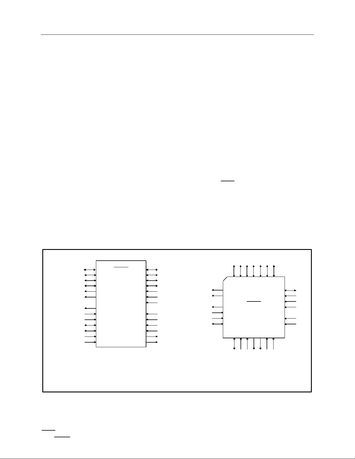
IA82050 Package Pinout
(17)
(16)
RTSn
DTRn or TB
D1
(18)
RESET
CSn
(25)
(24)
(23)
(22)
(21)
(20)
(19)
D0
A2
A1
A0
VDD
RDn
WRn
IA82050
(1)D4
(2)D5
28 Pin DIP
(3)D6
(4)D7
(5)INT
(6)TXD
(7)VSS
(8)X2 or OUT2n
(9)X1 or CLK
(10)SCLK or RIn
(11)DSRn or TA or OUT0n
(12)DCDn or ICLK or OUT1n
(13)RXD
(14)CTSn
(28) D3
(27) D2
(26) D1
(25) D0
(24) A2
(23) A1
(22) A0
(21) VDD
(20) RDn
(19) WRn
(18) CSn
(17) RESET
(16) RTSn
(15) DTRn or TB
(4)D7(3)D6(2)D5(1)D4(28)D3(27)D2(26)
(5)INT
(6)TXD
(7)VSS
(8)X2 or OUT2n
(9)X1 or CLK
(10)SCLK or RIn
(11)DSRn or TA or OUT0n
IA82050
28 Pin LCC
(15)
(14)
(13)
(12)
RXD
CTSn
DCDn or ICLK or OUT1n
Copyright 2001 ENG211010326-00 www.innovasic.com
innovASIC Customer Support:
The End of Obsolescence Page 1 of 11 1-888-824-4184
Page 2
IA82050 Data Sheet
ASYNCHRONOUS SERIAL CONTROLLER As of Production Ver. 01
DESCRIPTION
The IA82050 is an asynchronous serial controller that provides a CPU interface to one transmit
and one receive channel. It is Form, Fit, and Function compatible with the Intel 82050 and
82510. Configuration registers are used to control the serial channel, interrupts, and modes of
operation. The CPU controls this device via address and data lines with read/write control. The
CPU also uses this interface to read and write data to receive and transmit data through the serial
channel. FIFOs and various serial modes can be used to help off-load the CPU from transmitting
and receiving data. An interrupt line provides an indication to the CPU that the device requires
servicing. The device can be configured for 8250A/16450 compatibility.
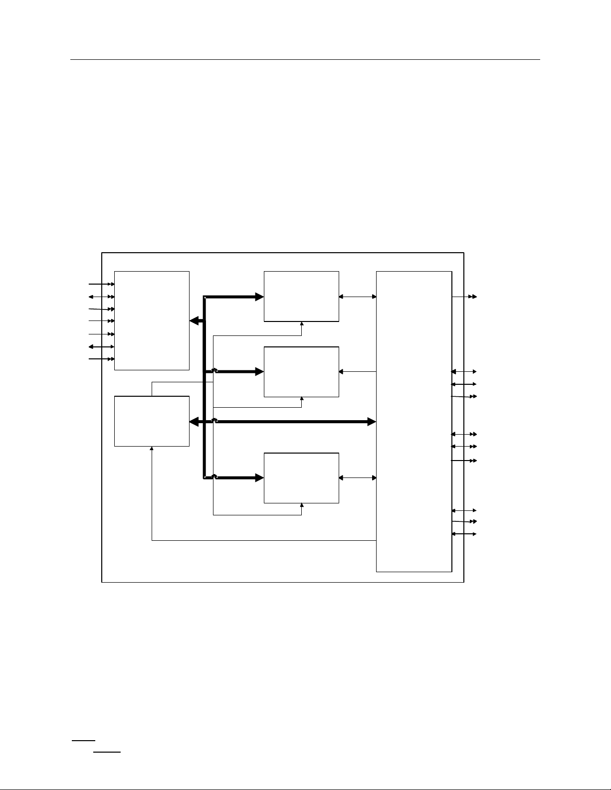
Functional Block Diagram
A(2:0)
D(7:0)
RDn
WRn
CSn
INT
RESET
BUS INTERFACE
(Reset Logic,
Registers,
Interrupt Generation,
TIMING
(Baud Rate
Generators A & B,
Clocking
CONFIG., STATUS, RXDATA
TXDATA
IA82050
TRANSMITTER
RECEIVER
TXD
RXD
CTSn
RTSn
PIN
CONFIGURATION
DSRn or TA or OUT0n
DCDn or ICLK or OUT1n
DTRn or TB
MODEM
X1 or CLK
X2 or OUT2n
SCLK or RIn
Copyright 2001 ENG211010326-00 www.innovasic.com
innovASIC Customer Support:
The End of Obsolescence Page 2 of 11 1-888-824-4184
Page 3

IA82050 Data Sheet
ASYNCHRONOUS SERIAL CONTROLLER As of Production Ver. 01
Functional Overview
Transmitter
The Transmit function consists of a 4 × 11 bit FIFO, and a Transmit Engine. The 4 × 11 FIFO is
configurable as any depth between one and four words inclusive. The transmit engine is
responsible for reading the data out of the FIFO and placing it in the proper order on the TXD pin.
The transmit engine is highly configurable to be compatible with numerous formats, including
16450 and 8250 modes of communication. Transmit Communication parameters that can be
programmed include:
• Parity modes
• Stop Bits
• Character Length
• FIFO Depth
• Clocking Options
• RTS and CTS modes
See the Register Description for more details.
Receiver
The Receiver function consists of a 4 × 11 configurable FIFO and a Receive Engine. The receive
engine is responsible for sampling the data on the RXD input pin, formatting the data, and placing
the data in the FIFO. The receive engine is highly configurable with parameters that include:
• Parity modes
• Stop Bits
• Character Length
• FIFO Depth
• Clocking Options
• Address Matching Options
• Control Character Detection
• RTS and CTS modes
See the Register Description for more details.
Bus Interface
The Bus Interface is a simple interface that allows a micro-processor or micro-controller to read
and write the IA82050 Registers. It consists of the following I/O lines:
• A0, A1, A2 : 3 Bit Address
• D0-D7 : 8 Bit Data
• RDn: Active Low Read Enable
• WRn: Active Low Write Enable
• CSn: Active Low Chip Select
• INT: Interrupt Output
• RESET: Chip Reset
Copyright 2001 ENG211010326-00 www.innovasic.com
innovASIC Customer Support:
The End of Obsolescence Page 3 of 11 1-888-824-4184
Page 4
IA82050 Data Sheet
ASYNCHRONOUS SERIAL CONTROLLER As of Production Ver. 01
Register Description
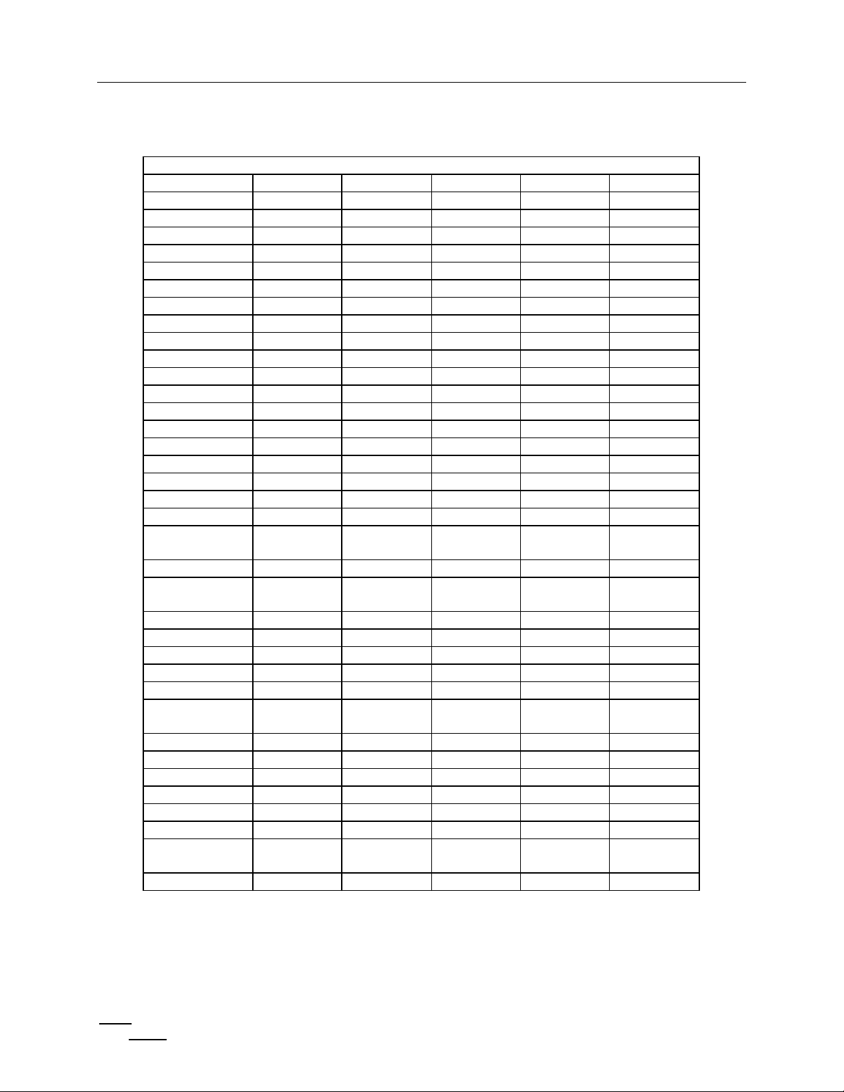
Table 1 – IA82050 Register Summary
Register ADDR Bank DLAB Mode Default
ACR0 111 00 X R/W 00000000
ACR1 101 10 X R/W 00000000
BACF 001 11 0 R/W 00000100
BAH 001 00 1 R/W 00000000
BAL 000 00 1 R/W 00000010
BANK 010 X X W 00000000
BBCF 011 11 X R/W 10000100
BBH 001 11 1 R/W 00000000
BBL 000 11 1 R/W 00000101
CLCF 000 11 0 R/W 00000000
FLR 100 01 X R 00000000
FMD 001 10 X R/W 00000000
GER 001 00 0 R/W 00000000
GIR_BANK 010 X X R 00000001
GSR 111 01 X R 00010010
ICM 111 01 X W N/A
IMD 100 10 X R/W 00001100
LCR 011 00 X R/W 00000000
LSR 101 00 X R/W 01100000
MCR 100
100
MIE 101 11 X R/W 00001111
MSR 110
110
PMD 100 11 X R/W 11111100
RCM 101 01 X W N/A
RIE 110 10 X R/W 00011110
RMD 111 10 X R/W 00000000
RST 101 01 X R 00000000
RXDATA 000
RXF 001 01 X R Unknown
TCM 110 01 X W N/A
TMCR 011 01 X W N/A
TMD 011 10 X R/W 00000000
TMIE 110 11 X R/W 00000000
TMST 011 01 X R 00110000
TXDATA 000
TXF 001 01 X W N/A
00
01
00
01
00
01
00
01
X
X
X
X
0
X
0
X
R/W
W
R/W
R
R Unknown
W N/A
00000000
00000000
Copyright 2001 ENG211010326-00 www.innovasic.com
innovASIC Customer Support:
The End of Obsolescence Page 4 of 11 1-888-824-4184
Page 5

IA82050 Data Sheet
ASYNCHRONOUS SERIAL CONTROLLER As of Production Ver. 01
AC/DC Parameters
Absolute maximum ratings:
Supply Voltage, VDD…………………………….…-0.3V to +6.0V
Input Voltage, VIN…………………………………-0.3V to VDD +0.3V
Input Pin Current, IIN…………………………….±10 mA, 25° C
Operating Temperature Range……………………..-40° C to +85°C
Ambient temperature under bias........................……..-40°C to +85°C *
Storage temperature.......................................…........….- 55°C to +150°C
Lead Temperature………………………………….+300°C, 10 sec.
Power dissipation..............................................................155 mW, 125°C, 25MHz, 15% Toggle
Stresses beyond those listed under “absolute maximum ratings” may cause permanent damage to the device. Operating the device beyond the conditions
indicated in the “recommended operating conditions” section is not recommended. Operation at the “absolute maximum ratings” may adversely affect
device reliability.
* The input and output parametric values in section VII-B, parts 1, 2, and 3, are directly related to ambient
temperature and DC supply voltage. A temperature or supply voltage range other than those specified in the
Operating Conditions above will affect these values and pa rt performance is not guaranteed by innovASIC.
Copyright 2001 ENG211010326-00 www.innovasic.com
innovASIC Customer Support:
The End of Obsolescence Page 5 of 11 1-888-824-4184
Page 6

IA82050 Data Sheet
OH
Static IDD current is exclusive of input/output drive requirements and is
ASYNCHRONOUS SERIAL CONTROLLER As of Production Ver. 01
DC Characteristics
Symbol Parameter Notes Min Max Unit
V
V
V
V
V
I
I
I
I
I
I
I
C
C
C
IL
IH1
IH2
OL
OH
LI
LO
CC
PU
STBY
OHR
OLR
IN
IO
XTAL
Input Low Voltage (1) -0.5 0.7 V
Input High Voltage-Cerdip (1) 2.1 VDD+.07 V
Input High Voltage-LCC (2) 2.1
VDD+.07
V
Output Low Voltage (2), (8) 0.4 V
Output High Voltage (3), (8) 2.4 V
Input Leakage Current (4) ±1 µA
3-State Leakage Current (5)
Power Supply Current (6)
Strapping Pullup Resistor (12)
Standby Supply Current (9)
RTSn, DTRn Strapping Current (10)
RTSn, DTRn Strapping Current (11)
Input Capacitance (7)
I/O Capacitance (7)
X1, X2 Load
±1
1.12
-283 -137
100
1.92
N/A
5
6
6
µA
mA/MHz
A
µA
mA
mA
pF
pF
pF
NOTES:
1. Does not apply to CLK/X1 pin, when configured as crystal oscillator input (X1).
2. @ IOL = 1.92 mA
3. @ I
= 1.92 mA
4. 0< VIN < VCC .
5. 0.4V < V
6. VDD = 5.5V, VIL= 0.7V (max), VIH = VDD - 0.7V (min), Typ. Val = 1.12 mA/MHz (Not Tested), Ext. 1X CLK, IOL = IOH = 0.
< VCC - 0.4V
OUT
7. Freq. = 1MHz.
8. Does not apply to OUT2/X2 pin, when configured as crystal oscillator output (X2).
9. Freq. = 1MHz. But, input clock not running.
measured with the clocks stopped and all inputs tied to VDD or VSS, configured
to draw minimum current.
10. Applies only during hardware reset for clock configuration options. Strapping current for logic HIGH.
11. Applies only during hardware reset for clock configuration options. Strapping current for logic LOW
12. Inputs (RTSn, DTRn, TB) with Pullups tested @ Vin = 0.0V VDD = 5.5V
Copyright 2001 ENG211010326-00 www.innovasic.com
innovASIC Customer Support:
The End of Obsolescence Page 6 of 11 1-888-824-4184
Page 7

IA82050 Data Sheet
ASYNCHRONOUS SERIAL CONTROLLER As of Production Ver. 01
AC Characteristics
Parameter Min Max Notes
CLK period 54 ns 250 ns Divide by Two
CLK period 54 ns 108 ns No Divide by
CLK Low Time 25 ns
CLK High Time 25 ns
10 ns Divide by Two
Measured between 0.3 * VDD
CLK Rise Time
10 ns Divide by Two
CLK Fall Time
CLK Rise Time 15 ns No Divide by
CLK Fall Time 15 ns No Divide by
Crystal Frequency 1 Mhz 20 Mhz
Reset Width 8 * Clock Period
RTS/DTR Low Setup
to Reset inactive
RTS/DTR Low Hold
after Reset inactive
RDn Active Width
Address/CSn Setup
Time to RDn Active
Address/CSn Hold
after RDn Inactive
RDn or WRn Inactive
to Active Delay
Data Out Float Delay
after RDn Inactive
WRn Active Width
Address CSn Setup
Time to WRn Active
Address and CSn hold
Time after WRn
Data in Setup Time to
WRn Inactive
Data In Hold Time after
WRn Inactive
SCLK Period 216 ns 16x Clocking Mode
SCLK Period 3500 ns 1x Clocking Mode
RXD Setup Time to
SCLK High
RXD Hold Time after
SCLK High
TXD Valid after SCLK
Low
TXD Delay after RXD 170 ns Remote Loopback
6 * Clock Period
Clock Period – 20 ns
2* clock period +
65 ns
7 ns
0 ns
Clock Period +
15 ns
40 ns
2 * Clock Period
+ 15 ns
7 ns
0 ns
90 ns
12 ns
250 ns
250 ns
170 ns
and 0.7 * VDD
Measured between 0.3 * VDD
and 0.7 * VDD
Copyright 2001 ENG211010326-00 www.innovasic.com
innovASIC Customer Support:
The End of Obsolescence Page 7 of 11 1-888-824-4184
Page 8

IA82050 Data Sheet
D
ASYNCHRONOUS SERIAL CONTROLLER As of Production Ver. 01
Packaging Information
PLCC Package
PIN 1
2 PLCS
1.22/1.07
E3
IDENTIFIER & ZONE
E
E1
D1
D3
TOP VIEW
BOTTOM VIEW
.81 / .66
SEATING PLANE
A
A1
e
.51 MIN.
.53 / .33
R 1.14 / .64
.10
LEAD COUNT
28 (in Millimeters)
Symbol
A 4.20 4.57
A1 2.29 3.04
D1 11.43 11.58
D2 9.91 10.92
D3 7.62 BSC
E1 11.43 11.58
E2 9.91 10.92
MIN MAX
D2 / E2
SIDE VIEW
Copyright 2001 ENG211010326-00 www.innovasic.com
E3 7.62 BSC
e 1.27 BSC
D 12.32 12.57
E 12.32 12.57
innovASIC Customer Support:
The End of Obsolescence Page 8 of 11 1-888-824-4184
Page 9

IA82050 Data Sheet
TOP
ASYNCHRONOUS SERIAL CONTROLLER As of Production Ver. 01
PDIP Package
E1 E
LEAD 1
IDENTIFIER
1
LEAD COUNT
DIRECTION
eA
eB
SIDE VIEW (WIDTH)
C
Lead Count
D
B
B1
e
A
Symbol
A - .200
A1 .015 -
B .015 .020
A1
L
B1 .050 .070
C .008 .012
D 1.380 1.470
E .580 .610
E1 .520 .560
e .100 TYP
28 (in Inches)
MIN MAX
SIDE VIEW (LENGTH)
eA .580 -
eB - .686
L .100 MIN
B2 - -
S - -
Copyright 2001 ENG211010326-00 www.innovasic.com
innovASIC Customer Support:
The End of Obsolescence Page 9 of 11 1-888-824-4184
Page 10

IA82050 Data Sheet
ASYNCHRONOUS SERIAL CONTROLLER As of Production Ver. 01
Ordering Information
Production Version 01
Order Number Environment Package Type
IA82050-PDW28I-01
IA82050-PDW28C-01
IA82050-PLC28I-01 Industrial
IA82050-PLC28C-01
Industrial
Commercial
Commercial
28 Lead Plastic DIP, 600 mil wide
28 Lead Plastic Leaded Chip Carrier
Copyright 2001 ENG211010326-00 www.innovasic.com
innovASIC Customer Support:
The End of Obsolescence Page 10 of 11 1-888-824-4184
Page 11

IA82050 Data Sheet
ASYNCHRONOUS SERIAL CONTROLLER As of Production Ver. 01
ERRATA
Production Version 01
1. Issue: Issuing more than one command via the Receive Command register (RCM) may
result in an unintended lock of the RX FIFO.
Workaround: If multiple commands via the RCM are required, execute them individually.
2. Issue: In semi-automatic and automatic transmit mode, RTS will assert at the same time as
the beginning of the start bit on TXD. If RTS is used to turn on the TXD line driver, the
width of the start bit could be distorted.
Workaround: Manual assertion of RTS and initiation of the transmit will avoid this issue.
Copyright 2001 ENG211010326-00 www.innovasic.com
innovASIC Customer Support:
The End of Obsolescence Page 11 of 11 1-888-824-4184
 Loading...