

Datasheet IA8044-PDW40I-01, IA8044-PLC40I-01, IA8344-PDW40I-01, IA8344-PLC40I-01 Datasheet (INOVC)
Page 1

IA8044/IA8344 Data Sheet
SDLC COMMUNICATIONS CONTROLLER
Copyright 2003 ENG210010112-00 www.innovasic.com
innovASIC Customer Support:
The End of Obsolescence Page 1 of 49 1-888-824-4184
FEATURES
• Form, Fit, and Function Compatible with the Intel 8044/8344
• Packaging options available: 40 Pin Plastic Dual In-Line Package (PDIP),
44 Pin Plastic Leaded Chip Carrier (PLCC)
• 8-Bit Control Unit
• 8-Bit Arithmetic-Logic Unit with 16-Bit multiplication and division
• 12 MHz clock
• Four 8-Bit Input / Output ports
• Two 16-Bit Timer/Counters
• Serial Interface Unit with SDLC/HDLC compatibility
• 2.4 Mbps maximum serial data rate
• Two Level Priority Interrupt System
• 5 Interrupt Sources
• Internal Clock prescaler and Phase generator
• 192 Bytes of Read/Write Data Memory Space
• 64kB External Program Memory Space
• 64kB External Data Memory Space
• 4kB Internal ROM (IA8044 only)
IA8044/IA8344 Variants
IA8044
4kB internal ROM with R0117 version 2.3 firmware, 192 byte internal RAM,
64kB external program and data space.
IA8344 192 byte internal RAM, 64kB external program and data space.
The IA8044/IA8344 is a "plug-and-play" drop-in replacement for the original IC. InnovASIC
produces replacement ICs using its MILESTM, or Managed IC Lifetime Extension System, cloning
technology. This technology produces replacement ICs far more complex than "emulation" while
ensuring they are compatible with the original IC. MILESTM captures the design of a clone so it can
be produced even as silicon technology advances. MILESTM also verifies the clone against the
original IC so that even the "undocumented features" are duplicated. This data sheet documents all
necessary engineering information about the IA8044/IA8344 including functional and I/O
descriptions, electrical characteristics, and applicable timing.
innovASIC
Page 2
IA8044/IA8344 Data Sheet
SDLC COMMUNICATIONS CONTROLLER
Copyright 2003 ENG210010112-00 www.innovasic.com
innovASIC Customer Support:
The End of Obsolescence Page 2 of 49 1-888-824-4184
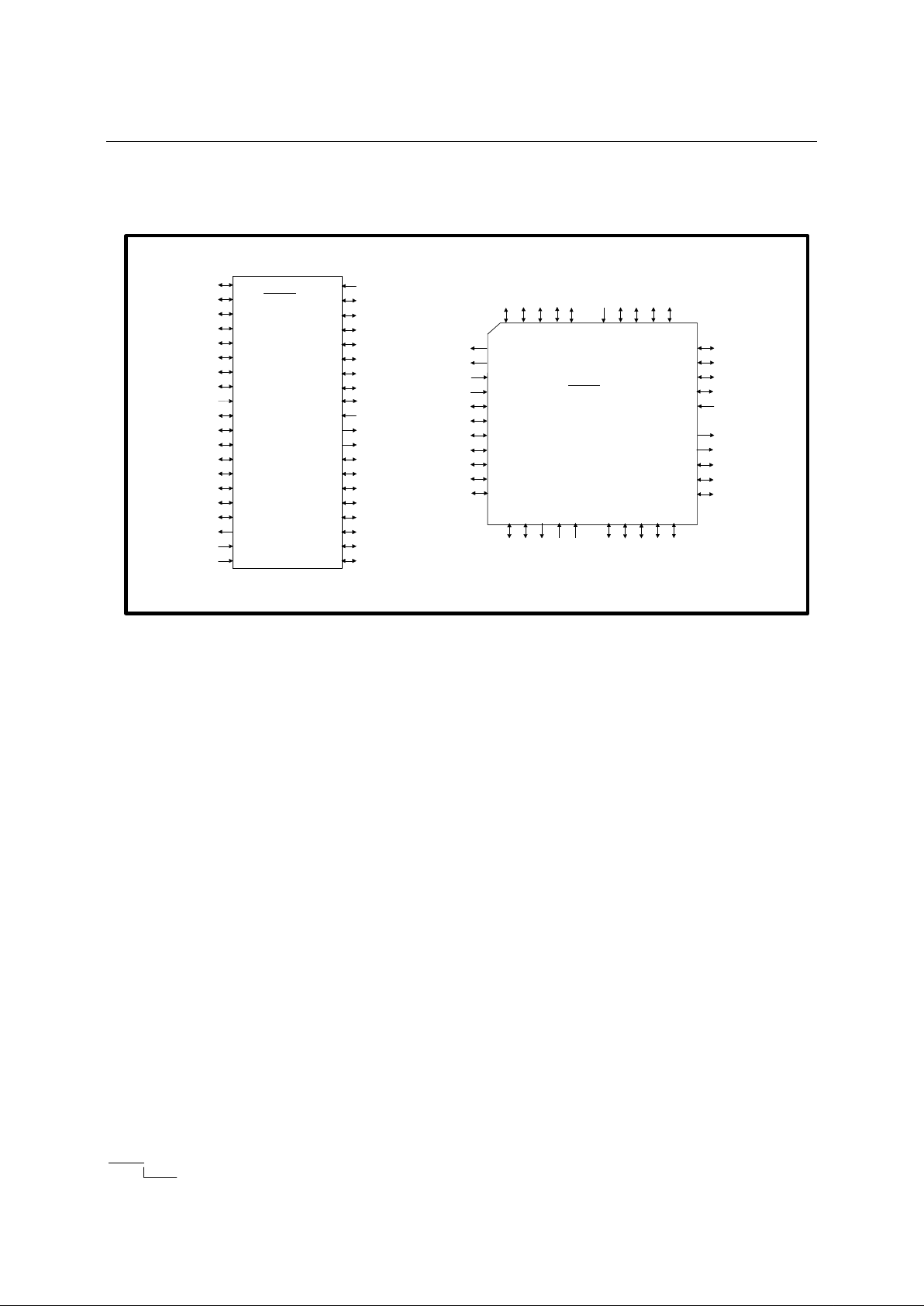
Package Pinout
(6)P1.5
(1)P1.0
(2)P1.1
(3)P1.2
(4)P1.3
(5)P1.4
(7)(RTS) P1.6
(8)
(9)RST
(10)
(11)
(12)(INT0) P3.2
(13)
(INT1) P3.3
(14)
40 Pin DIP
IA8X44
P0.7 (AD7)
EA
ALE
PSEN
(20)VSS
(15)
(SCLK/T1) P3.5
(16)
(WR) P3.6
(17)
(RD) P3.7
(18)
XTAL2
(19)XTAL1
(21)
(22)
(23)
(24)
P2.1 (A9)
P2.0 (A8)
(40)
(39)
(38)
(37)
(36)
(35)
(34)
(33)
(32)
(31)
(30)
(29)
(28)
(27)
(26)
(25)
(T0) P3.4
P2.3 (A11)
P2.2 (A10)
P2.5 (A13)
P2.4 (A12)
P2.7 (A15)
P2.6 (A14)
P0.5 (AD5)
P0.6 (AD6)
P0.3 (AD3)
P0.4 (AD4)
P0.1 (AD1)
P0.2 (AD2)
VCC
P0.0 (AD0)
(CTS) P1.7
(RXD) P3.0
(TXD) P3.1
P1.3
P1.4
P3.6
P2.6
44 Pin LCC
IA8X44
(12)N.C.
(7)P1.5
(8)P1.6
(9)P1.7
(10)RST/VPD
(11)P3.0
(13)P3.1
(14)P3.2
(15)P3.3
(16)P3.4
(17)P3.5
P0.4
ALE
N.C.
EA
P0.6
P0.5
XTAL2
P3.7
(6)
(5)
(4)
(3)
(2)
(1)
(44)
(43)
(42) P0.1
(41) P0.2
(40) P0.3
(34)
(39)
(38)
(37)
(36)
(35)
(33)
(32)
(31)
(30)
(29)
(18)
(19)
(20)
(21)
(22)
(23)
(24)
(25)
(26)
(27)
(28)
VCC
P0.0
P1.0
N.C.
P1.2
P1.1
VSS
XTAL1
P2.0
N.C.
P2.2
P2.1
P2.4
P2.3
P2.5
P2.7
PSEN
P0.7
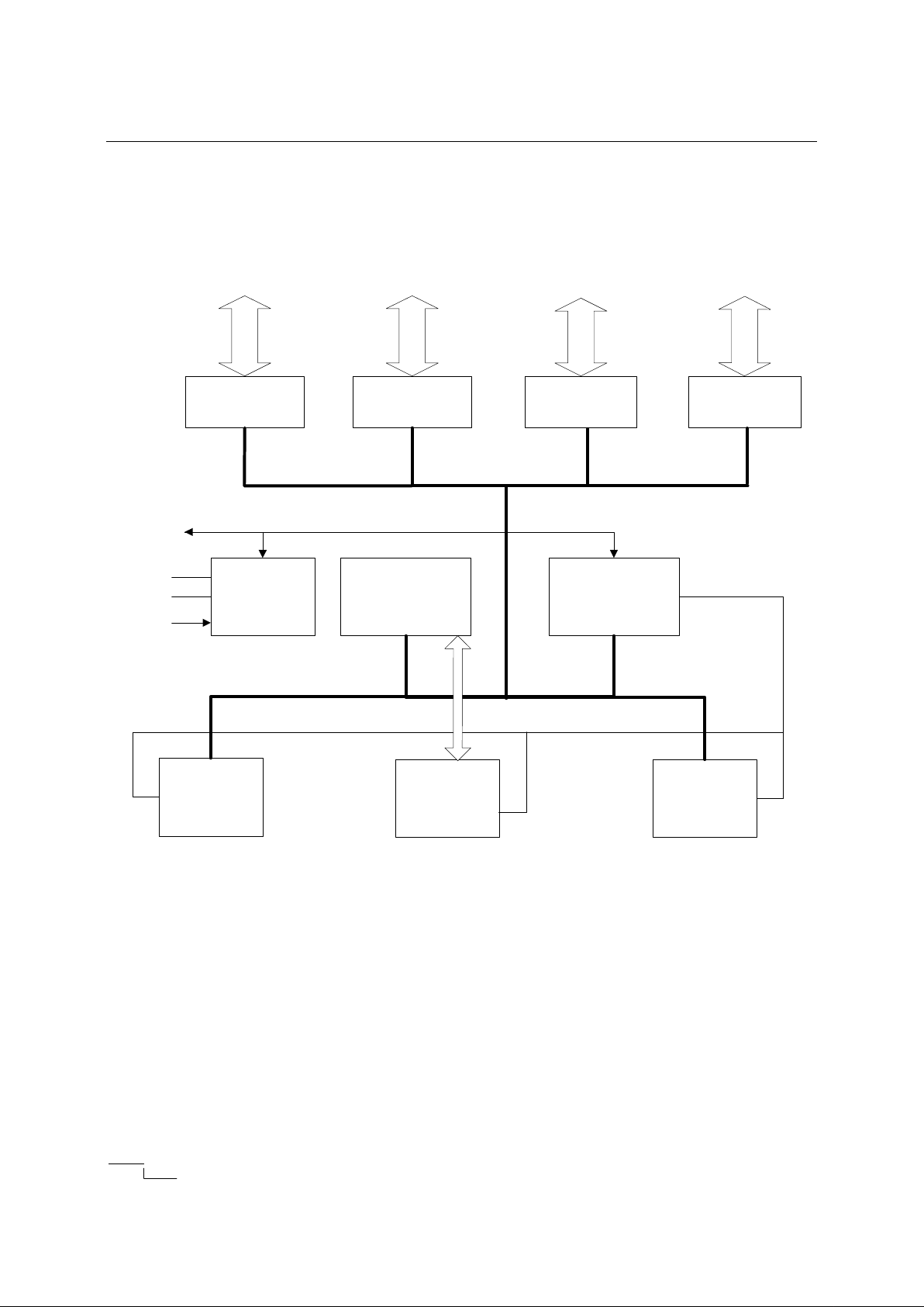
DESCRIPTION
The IA8044/IA8344 is a form, fit and function compatible part to the Intel 8X44 SDLC
communications controller. The IA8044/IA8344 is a Fast Single-Chip 8-Bit Microcontroller with an
integrated SDLC/HDLC serial interface controller. The IA8044/IA8344 is a fully functional 8-Bit
Embedded Controller that executes all ASM51 instructions and has the same instruction set as the
Intel 80C51. The IA8044/IA8344 can access the instructions from two types of program memory,
serves software and hardware interrupts, provides an interface for serial communications and a timer
system. The IA8044/IA8344 is fully compatible with the Intel 8X44 series. The functional block
diagram is shown below.
Page 3
IA8044/IA8344 Data Sheet
SDLC COMMUNICATIONS CONTROLLER
Copyright 2003 ENG210010112-00 www.innovasic.com
innovASIC Customer Support:
The End of Obsolescence Page 3 of 49 1-888-824-4184
Functional Block Diagram
192x8Dual Port
RAM
C8051
CPU
Interrupts
Timers
Port 0
ADDR/DATA/IO
Port 2
ADDR/DATA/IO
Port 1
SPCL FUNC/IO
Port 3
SPCL FUNC/IO
SIU
Control
Address/Data
Clock Gen.
& Timing
XTAL
Reset
Memory
Control
I/O for Memory, SIU, DMA, Interrupts, Timers
Page 4
IA8044/IA8344 Data Sheet
SDLC COMMUNICATIONS CONTROLLER
Copyright 2003 ENG210010112-00 www.innovasic.com
innovASIC Customer Support:
The End of Obsolescence Page 4 of 49 1-888-824-4184
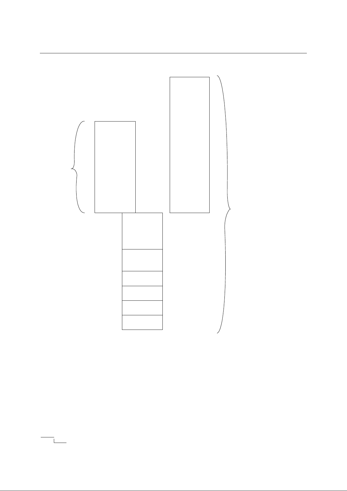
I/O Characteristics
The table below describes the I/O characteristics for each signal on the IC. The signal names
correspond to the signal names on the pinout diagrams provided. The table below provides the I/O
description of the IA8044 and the IA8344.
Name Type Description
RST I Reset. This pin when held high for two machine cycles while
the oscillator is running will cause the chip to reset.
ALE O Address Latch Enable. Used to latch the address on the falling
edge for external memory accesses.
PSEN O Program Store Enable. When low acts as an output enable for
external program memory.
EA I External Access. When held low EA will cause the
IA8044/IA8344 to fetch instructions from external memory.
P0.7 – P0.0 I/O Port 0. 8 bit I/O port and low order multiplexed address/data
byte for external accesses.
P1.7 – P1.0 I/O Port 1. 8-bit I/O port. Two bits have alternate functions, P1.6
(RTS) and P1.7 (CTS).
P2.7 – P2.0 I/O Port 2. 8-bit I/O port. It also functions as the high order
address byte during external accesses.
P3.7 – P3.0 I/O Port 3. 8-bit I/O port. Port 3 bits also have alternate functions
as described below.
P3.0 – RXD. Receive data input for SIU or direction control
for P3.1 dependent upon datalink configuration.
P3.1 – TXD. Transmit data output for SIU or data
input/output dependent upon datalink configuration. Also
enables diagnostic mode when cleared.
P3.2 – INT0. Interrupt 0 input or gate control input for counter
0.
P3.3 – INT1. Interrupt 1 input or gate control input for counter
1.
P3.4 – T0. Input to counter 0.
P3.5 – SCLK/T1. SCLK input to SIU or input to counter 1.
P3.6 – WR. External memory write signal.
P3.7 – RD. External memory read signal.
XTAL1 I Crystal Input 1. Connect to VSS when external clock is used on
XTAL2. May be connected to a crystal (with XTAL2), or may
be driven directly with a clock source (XTAL2 not connected).
XTAL2 O Crystal Input 2. May be connected to a crystal (with XTAL1),
or may be driven directly with an inverted clock source (XTAL1
tied to ground).
VSS P Ground.
VCC P +5V power.
Page 5
IA8044/IA8344 Data Sheet
SDLC COMMUNICATIONS CONTROLLER
Copyright 2003 ENG210010112-00 www.innovasic.com
innovASIC Customer Support:
The End of Obsolescence Page 5 of 49 1-888-824-4184
Memory Organization
Program Memory
Program Memory includes interrupt and Reset vectors. The interrupt vectors are spaced at 8byte intervals, starting from 0003H for External Interrupt 0.
Reset Vectors
These locations may be used for program code, if the corresponding interrupts are not used
(disabled). The Program Memory space is 64K, from 0000H to FFFFH. The lowest 4K of program
code (0000H to 0FFFH) can be fetched from external or internal Program Memory. This selection is
made by strapping pin ‘EA’ (External Address) to GND or VCC. If during reset, ‘EA’ is held low,
all the program code is fetched from external memory. If, during reset, ‘EA’ is held high, the lowest
4K of program code (0000H to 0FFFH) is fetched from internal memory (ROM). Program
memory addresses above 4K (0FFFH) will cause the program code to be fetched from external
memory regardless of the setting of ‘EA’.
Data Memory
External Data Memory
The IA8044/IA8344 Microcontroller core incorporates the Harvard architecture, with separate
code and data spaces. The code from external memory is fetched by ‘psen’ strobe, while data
is read from RAM by bit 7 of P3 (read strobe) and written to RAM by bit 6 of P3 (write strobe). The
External Data Memory space is active only by addressing through use of the MOVX instruction and
the 16-bit Data Pointer Register (DPTR). A smaller subset of external data memory (8 bit
addressing) may be accessed by using the MOVX instruction with register indexed addressing.
Internal Data Memory
The Internal Data Memory address is always 1 byte wide. The memory space is 192 bytes
large (00H to BFH), and can be accessed by either direct or indirect addressing. The Special
Function Registers occupy the upper 128 bytes. This SFR area is available only by direct
addressing. Internal memory that overlaps the SFR address space is only accessible by indirect
addressing.
Location Service
0003H External Interrupt 0
000BH Timer 0 overflow
0013H External Interrupt 1
001BH Timer 1 overflow
0023H SIU Interrupt
Page 6
IA8044/IA8344 Data Sheet
SDLC COMMUNICATIONS CONTROLLER
Copyright 2003 ENG210010112-00 www.innovasic.com
innovASIC Customer Support:
The End of Obsolescence Page 6 of 49 1-888-824-4184
Internal Memory
8044 Internal Data Memory Addresses
00h to FFh
80h
FFh
80h
BFh
Indirect
Addressing
RAM
00h
07h
08h
17h
18h
1Fh
20h
2Fh
30h
7Fh
10h
0Fh
Register Bank 0
Register Bank 1
Register Bank 2
Register Bank 3
Bit Addressable
Memory
Internal Data Ram
Direct Addressing
Special Function
Registers
Addressable
BITS in SFRs
(128 BITS)
Page 7

IA8044/IA8344 Data Sheet
SDLC COMMUNICATIONS CONTROLLER
Copyright 2003 ENG210010112-00 www.innovasic.com
innovASIC Customer Support:
The End of Obsolescence Page 7 of 49 1-888-824-4184
Bit Addressable Memory
Both the internal RAM and the Special Function Registers have locations that are bit addressable in
addition to the byte addressable locations.
SFR Bit Addressable Locations
Byte Address bit 7 bit 6 bit 5 bit 4 bit 3 bit 2 bit 1 bit 0 Register
F0h F7h F6h F5h F4h F3h F2h F1h F0h B
E0h E7h E6h E5h E4h E3h E2h E1h E0h ACC
D8h DFh DEh DDh DCh DBh DAh D9h D8h NSNR
D0h D7h D6h D5h D4h D3h D2h D1h D0h PSW
C8h CFh CEh CDh CCh CBh CAh C9h C8h STS
B8h - - - BCh BBh BAh B9h B8h IP
B0h B7h B6h B5h B4h B3h B2h B1h B0h P3
A8h AFh - - ACh ABh AAh A9h A8h IE
A0h A7h A6h A5h A4h A3h A2h A1h A0h P2
90h 97h 96h 95h 94h 93h 92h 91h 90h P1
88h 8Fh 8Eh 8Dh 8Ch 8Bh 8Ah 89h 88h TCON
80h 87h 86h 85h 84h 83h 82h 81h 80h P0
Internal RAM Bit Addressable Locations
Byte Address bit 7 bit 6 bit 5 bit 4 bit 3 bit 2 bit 1 bit 0
30h-BFh Upper Internal Ram locations
2Fh 7Fh 7Eh 7Dh 7Ch 7Bh 7Ah 79h 78h
2Eh 77h 76h 75h 74h 73h 72h 71h 70h
2Dh 6Fh 6Eh 6Dh 6Ch 6Bh 6Ah 69h 68h
2Ch 67h 66h 65h 64h 63h 62h 61h 60h
2Bh 5Fh 5Eh 5Dh 5Ch 5Bh 5Ah 59h 58h
2Ah 57h 56h 55h 54h 53h 52h 51h 50h
29h 4Fh 4Eh 4Dh 4Ch 4Bh 4Ah 49h 48h
28h 47h 46h 45h 44h 43h 42h 41h 40h
27h 3Fh 3Eh 3Dh 3Ch 3Bh 3Ah 39h 38h
26h 37h 36h 35h 34h 33h 32h 31h 30h
25h 2Fh 2Eh 2Dh 2Ch 2Bh 2Ah 29h 28h
24h 27h 26h 25h 24h 23h 22h 21h 20h
23h 1Fh 1Eh 1Dh 1Ch 1Bh 1Ah 19h 18h
22h 17h 16h 15h 14h 13h 12h 11h 10h
21h 0Fh 0Eh 0Dh 0Ch 0Bh 0Ah 09h 08h
20h 07h 06h 05h 04h 03h 02h 01h 00h
18h-1Fh Register Bank 3
10h-17h Register Bank 2
08h-0Fh Register Bank 1
00h-07h Register Bank 0
Page 8

IA8044/IA8344 Data Sheet
SDLC COMMUNICATIONS CONTROLLER
Copyright 2003 ENG210010112-00 www.innovasic.com
innovASIC Customer Support:
The End of Obsolescence Page 8 of 49 1-888-824-4184
Instruction Set
The 8X44 architecture and instruction set are identical to the 8051’s. The following tables give a
survey of the instruction set of the IA8044/IA8344 Microcontroller core.
Arithmetic Operations
Mnemonic
Description
Byte
Cycle
ADD A,Rn
Add register to accumulator
1 1
ADD A, direct
Add direct byte to accumulator
2 1
ADD A,@Ri
Add indirect RAM to accumulator
1 1
ADD A,#data
Add immediate data to accumulator
2 1
ADDC A,Rn
Add register to accumulator with carry flag
1 1
ADDC A,direct
Add direct byte to A with carry flag
2 1
ADDC A,@Ri
Add indirect RAM to A with carry flag
1 1
ADDC A,#data
Add immediate data to A with carry flag
2 1
SUBB A,Rn Subtract register from A with borrow 1 1
SUBB A,direct Subtract direct byte from A with borrow 2 1
SUBB A,@Ri Subtract indirect RAM from A with borrow 1 1
SUBB A,#data Subtract immediate data from A with borrow 2 1
INC A Increment accumulator 1 1
INC Rn Increment register 1 1
INC direct Increment direct byte 2 1
INC @ Ri Increment indirect RAM 1 1
DEC A Decrement accumulator 1 1
DEC Rn Decrement register 1 1
DEC direct Decrement direct byte 2 1
DEC @Ri Decrement indirect RAM 1 1
INC DPTR Increment data pointer 1 2
MUL A,B Multiply A and B 1 4
DIV A,B Divide A by B 1 4
DA A Decimal adjust accumulator 1 1
Page 9

IA8044/IA8344 Data Sheet
SDLC COMMUNICATIONS CONTROLLER
Copyright 2003 ENG210010112-00 www.innovasic.com
innovASIC Customer Support:
The End of Obsolescence Page 9 of 49 1-888-824-4184
Logic Operations
Mnemonic
Description
Byte Cycle
ANL A,Rn
AND register to accumulator
1 1
ANL A,direct
AND direct byte to accumulator
2 1
ANL A,@Ri
AND indirect RAM to
accumulator 1 1
ANL A,#data
AND immediate data to accumulator
2 1
ANL direct,A
AND accumulator to direct byte
2 1
ANL direct,#data
AND immediate data to direct byte
3 2
ORL A,Rn OR register to accumulator 1 1
ORL A,direct OR direct byte to accumulator 2 1
ORL A,@Ri OR indirect RAM to accumulator 1 1
ORL A,#data OR immediate data to accumulator 2 1
ORL direct,A OR accumulator to direct byte 2 1
ORL direct,#data OR immediate data to direct byte 3 2
XRL A,Rn Exclusive OR register to accumulator 1 1
XRL A,direct Exclusive OR direct byte to accumulator 2 1
XRL A,@Ri Exclusive OR indirect RAM to accumulator 1 1
XRL A,#data Exclusive OR immediate data to accumulator 2 1
XRL direct,A Exclusive OR accumulator to direct byte 2 1
XRL direct,#data Exclusive OR immediate data to direct byte 3 2
CLR A Clear accumulator 1 1
CPL A Complement accumulator 1 1
RL A Rotate accumulator left 1 1
RLC A Rotate accumulator left through carry 1 1
RR A Rotate accumulator right 1 1
RRC A Rotate accumulator right through carry 1 1
SWAP A Swap nibbles within the accumulator 1 1
Page 10

IA8044/IA8344 Data Sheet
SDLC COMMUNICATIONS CONTROLLER
Copyright 2003 ENG210010112-00 www.innovasic.com
innovASIC Customer Support:
The End of Obsolescence Page 10 of 49 1-888-824-4184
Data Transfer
Mnemonic
Description
Byte
Cycle
MOV A,Rn Move register to accumulator 1 1
MOV A,direct Move direct byte to accumulator 2 1
MOV A,@Ri Move indirect RAM to accumulator 1 1
MOV A,#data Move immediate data to accumulator 2 1
MOV Rn,A Move accumulator to register 1 1
MOV Rn,direct Move direct byte to register 2 2
MOV Rn,#data Move immediate data to register 2 1
MOV direct,A Move accumulator to direct byte 2 1
MOV direct,Rn Move register to direct byte 2 2
MOV direct,direct Move direct byte to direct byte 3 2
MOV direct,@Ri Move indirect RAM to direct byte 2 2
MOV direct,#data Move immediate data to direct byte 3 2
MOV @Ri,A Move accumulator to indirect RAM 1 1
MOV @Ri,direct Move direct byte to indirect RAM 2 2
MOV @ Ri, #data Move immediate data to indirect RAM 2 1
MOV DPTR, #data16 Load data pointer with a 16-bit constant 3 2
MOVC A,@A + DPTR
Move code byte relative to DPTR to accumulator 1 2
MOVC A,@A + PC Move code byte relative to PC to accumulator 1 2
MOVX A,@Ri Move external RAM (8-bit addr.) to A 1 2
MOVX A,@DPTR Move external RAM (16-bit addr.) to A 1 2
MOVX @Ri,A Move A to external RAM (8-bit addr.) 1 2
MOVX @DPTR,A Move A to external RAM (16-bit addr.) 1 2
PUSH direct Push direct byte onto stack 2 2
POP direct Pop direct byte from stack 2 2
XCH A,Rn Exchange register with accumulator 1 1
XCH A,direct Exchange direct byte with accumulator 2 1
XCH A,@Ri Exchange indirect RAM with accumulator 1 1
XCHD X,@ Ri Exchange low-order nibble indir. RAM with A 1 1
Page 11
IA8044/IA8344 Data Sheet
SDLC COMMUNICATIONS CONTROLLER
Copyright 2003 ENG210010112-00 www.innovasic.com
innovASIC Customer Support:
The End of Obsolescence Page 11 of 49 1-888-824-4184
Boolean Manipulation
Mnemonic
Description
Byte Cycle
CLR C Clear carry flag 1 1
CLR bit Clear direct bit 2 1
SETB C Set carry flag 1 1
SETB bit Set direct bit 2 1
CPL C Complement carry flag 1 1
CPL bit Complement direct bit 2 1
ANL C,bit
AND direct bit to carry flag
2 2
ANL C,bit
AND complement of direct bit to carry
2 2
ORL C,bit OR direct bit to carry flag 2 2
ORL C,bit OR complement of direct bit to carry 2 2
MOV C,bit Move direct bit to carry flag 2 1
MOV bit,C Move carry flag to direct bit 2 2
Program Branches
Mnemonic
Description
Byte Cycle
ACALL addr11
Absolute
subroutine call 2 2
LCALL addr16 Long subroutine call 3 2
RET Return from subroutine 1 2
RETI Return from interrupt 1 2
AJMP addr11
Absolute jump
2 2
LJMP addr16 Long jump 3 2
SJMP rel Short jump (relative addr.) 2 2
JMP @A + DPTR
Jump
indirect relative to the DPTR 1 2
JZ rel
Jump if accumulator is zero
2 2
JNZ rel
Jump if accumulator is not zero
2 2
JC rel
Jump if carry flag is set
2 2
JNC rel
Jump if carry flag is not set
2 2
JB bit,rel
Jump if direct bit is set
3 2
JNB b
it,rel
Jump if direct bit is not set
3 2
JBC bit,rel
Jump if direct bit is set and clear bit
3 2
CJNE A,direct,rel Compare direct byte to A and jump if not equal 3 2
CJNE A,#data,rel Compare immediate to A and jump if not equal 3 2
CJNE Rn,#data rel Compare immed. to reg. and jump if not equal 3 2
CJNE @Ri,#data,rel Compare immed. to ind. and jump if not equal 3 2
DJNZ Rn,rel Decrement register and jump if not zero 2 2
DJNZ direct,rel Decrement direct byte and jump if not zero 3 2
NOP No operation 1 1
Page 12
IA8044/IA8344 Data Sheet
SDLC COMMUNICATIONS CONTROLLER
Copyright 2003 ENG210010112-00 www.innovasic.com
innovASIC Customer Support:
The End of Obsolescence Page 12 of 49 1-888-824-4184
Special Function Registers
The IA8044/IA8344 contains the following special function registers:
Symbol Register Description Byte
Address(Hex)
Bit Addresses (Hex)
(MSB - LSB)
ACC Accumulator E0h E7h – E0h
B B register F0h F7h – F0h
PSW Program Status Word D0h D7h – D0h
SP Stack Pointer 81h DPH Data Pointer High Byte 82h DPL Data Pointer Low Byte 83h P0 Port 0 80h 87h – 80h
P1 Port 1 90h 97h – 90h
P2 Port 2 A0h A7h – A0h
P3 Port 3 B0h B7h – B0h
IP Interrupt Priority B8h BCh – B8h
IE Interrupt Enable A8h AFh,ACh – A8h
TMOD Timer/Counter Mode 89h TCON Timer/Counter Control 88h 8Fh – 88h
TH0 Timer/Counter 0 high byte 8Ch TL0 Timer/Counter 0 low byte 8Ah TH1 Timer/Counter 1 high byte 8Dh TL1 Timer/Counter 1 low byte 8Bh SMD Serial Mode C9h STS SIU Status and Command C8h CFh – C8h
NSNR SIU Send/Receive Count D8h DFh – D8h
STAD SIU Station Address CEh TBS Transmit Buffer Start Address DCh TBL Transmit Buffer Length DBh TCB Transmit Control Byte DAh RBS Receive Buffer Start Address CCh RBL Receive Buffer Length CBh RFL Receive Field Length CDh RCB Receive Control Byte CAh DMA CNT DMA Count CFh FIFO FIFO contents (3 bytes) DF,DE,DDh SIUST SIU State Counter D9h -
Page 13

IA8044/IA8344 Data Sheet
SDLC COMMUNICATIONS CONTROLLER
Copyright 2003 ENG210010112-00 www.innovasic.com
innovASIC Customer Support:
The End of Obsolescence Page 13 of 49 1-888-824-4184
Ports
Ports P0, P1, P2 and P3 are Special Function Registers. The contents of the SFR can be observed on
corresponding pins on the chip. Writing a ‘1’ to any of the ports causes the corresponding pin to be
at high level (VCC), and writing a ‘0’ causes the corresponding pin to be held at low level (GND).
All four ports on the chip are bi-directional. Each of them consists of a Latch (SFR P0
to P3), an output driver, and an input buffer, so the CPU can output or read data through any
of these ports if they are not used for alternate purposes.
Ports P0, P1, P2 and P3 can perform some alternate functions. Ports P0 and P2 are
used to access external memory. In this case, port ‘p0’ outputs the multiplexed lower 8 bits of
address with ‘ale’ strobe high and then reads/writes 8 bits of data. Port P2 outputs the higher 8
bits of address. Keeping ‘ea’ pin low (tied to GND) activates this alternate function for ports
P0 and P2.
Port P3 and P1 can perform some alternate functions. The pins of Port P3 are multifunctional.
They can perform additional functions as described below.
Pin Symbol Function
P3.0 RxD, I/O In point-to-point or multipoint configurations (SMD.3 = 0) this pin
is I/O and signals the direction of data flow on DATA (P3.1). In loop mode
(SMD.3 = 1) and diagnostic mode this pin is RxD, Receive Data
input.
P3.1 TxD, DATA In point to point or multipoint configurations (SMD.3 = 0) this pin
is DATA and is the transmit/receive data pin. In loop mode
(SMD.3 = 1) this pin is the transmit data, TxD, pin. Writing a ‘0’ to
this port buffer bit enables the diagnostic mode.
P3.2 INT0 External interrupt 0 input. Also gate control input for counter 0.
P3.3 INT1 External interrupt 1 input. Also gate control input for counter 1.
P3.4 T0 Timer/Counter 0 external input. Setting the appropriate bits in the
Special Function Registers TCON and TMOD activates this
function.
P3.5 T1, SCLK Timer/Counter 1 external input. Setting the appropriate bits in the
Special Function Registers TCON and TMOD activates this
function. . Can also function as the external clock source for the SIU.
P3.6 WR External Data Memory write strobe, active LOW. This function
is activated by a CPU write access to External Data Memory
(i.e. MOVX @DPTR, A).
Page 14

IA8044/IA8344 Data Sheet
SDLC COMMUNICATIONS CONTROLLER
Copyright 2003 ENG210010112-00 www.innovasic.com
innovASIC Customer Support:
The End of Obsolescence Page 14 of 49 1-888-824-4184
P3.7 RD External Data Memory read strobe, active LOW. This function is
activated by a CPU read access from External Data Memory (i.e. MOVX
A, @DPTR).
P1.6 RTS Request To Send output, active low.
P1.7 CTS Clear To Send input, active low.
Port Registers
Port 0 (P0):
General purpose, 8 bit, I/O port and multiplexed low order address and data bus with open-drain
output buffers.
P0
Bit: 7 6 5 4 3 2 1 0
P0.7 P0.6 P0.5 P0.4 P0.3 P0.2 P0.1 P0.0
Port 1 (P1):
General purpose, 8 bit, I/O port with pullups and auxiliary functions.
P1
Bit: 7 6 5 4 3 2 1 0
RTS/P1.7 CTS/P1.6 P1.5 P1.4 P1.3 P1.2 P1.1 P1.0
P1.0 -
P1.1 -
P1.2 -
P1.3 -
P1.4 -
P1.5 -
P1.6 RTS Request To Send output.
P1.7 CTS Clear To Send input.
Port 2 (P2):
General purpose, 8 bit, I/O port with pullups and high order address bus.
P2
Bit: 7 6 5 4 3 2 1 0
P2.7 P2.6 P2.5 P2.4 P2.3 P2.2 P2.1 P2.0
Page 15

IA8044/IA8344 Data Sheet
SDLC COMMUNICATIONS CONTROLLER
Copyright 2003 ENG210010112-00 www.innovasic.com
innovASIC Customer Support:
The End of Obsolescence Page 15 of 49 1-888-824-4184
Port 3 (P3):
General purpose, 8-bit I/O port with pullups and auxiliary functions. Bits on this port also
functions as the SIU data transmit/receive I/O, external interrupt inputs, timer inputs and the read
and write strobes for external memory accesses.
P3
Bit: 7 6 5 4 3 2 1 0
RD WR T1 T0 INT1 INT0 TxD RxD
P3.0 RxD Serial input pin.
P3.1 TxD Serial output pin.
P3.2 INT0 External interrupt 0.
P3.3 INT1 External interrupt 1.
P3.4 T0 Timer/Counter 0 external input.
P3.5 T1 Timer/Counter 1 external input.
P3.6 WR External Data Memory write strobe, active LOW.
P3.7 RD External Data Memory read strobe, active LOW.
Page 16

IA8044/IA8344 Data Sheet
SDLC COMMUNICATIONS CONTROLLER
Copyright 2003 ENG210010112-00 www.innovasic.com
innovASIC Customer Support:
The End of Obsolescence Page 16 of 49 1-888-824-4184
Timers/Counters
Timers 0 and 1
The IA8X44 has two 16-bit timer/counter registers: Timer 0 and Timer 1. Both can be configured
for counter or timer operations. In timer mode, the register is incremented every machine cycle,
which means that it counts up after every 12 oscillator periods. In counter mode, the register is
incremented when the falling edge is observed at the corresponding input pin T0 or T1. Since it
takes 2 machine cycles to recognize a 1-to-0 event, the maximum input count rate is 1/24 of the
oscillator frequency. There are no restrictions on the duty cycle, however to ensure proper
recognition of 0 or 1 state, an input should be stable for at least 1 machine cycle (12 clock periods).
Four operating modes can be selected for Timer 0 and Timer 1. Two Special Function
Registers (TMOD and TCON) are used to select the appropriate mode.
Mode 0
In mode 0 the timers operate as an 8-bit timer (TH0/1) with a divide by 32 bit prescalar (TL0/1).
Mode 0 uses all 8 bits of TH0/1 and the lower 5 bits of TL0/1. The upper 3 bits of TL0/1 are
unknowns. Setting TR0/1 does not reset the registers TH0/1 and TL0/1. As the timer rolls over
from all 1’s to all 0’s it will set the interrupt flag TF0/1.
Mode 1
Mode 1 is the same as mode 0 except that all 8 bits of TL0/1 are used instead of just the lower 5
bits.
Mode 2
Mode 2 configures TL0/1 as an 8-bit counter with automatic reload from the contents of TH0/1.
Overflow of TL0/1 causes the interrupt TF0/1 to be set and the reload to occur. The contents of
TH0/1 are not affected by the reload.
Mode 3
Mode 3 creates two separate 8 bit counters from TL0 and TH0. TL0 uses the timer 0 mode bits
from TMOD, TMOD .0 through TMOD.3. TH0 is a timer only (not a counter) and uses timer 1’s
control bits, TR1 and TF1 for operation. Timer 1 can still be used if an interrupt is not required by
switching it in and out of its own mode 3. With TMOD.4 and TMOD.5 both high timer 1 will stop
and hold its count.
Timer Mode (TMOD):
The Timer Mode register contains bits that select the mode that the timers are to be operated in.
The lower nibble controls timer 0 and the upper nibble controls timer 1.
TMOD
Bit: 7 6 5 4 3 2 1 0
GATE C/T M1 M0 GATE C/T M1 M0
TMOD.0 M0 Timer 0 mode selector bit.
Page 17

IA8044/IA8344 Data Sheet
SDLC COMMUNICATIONS CONTROLLER
Copyright 2003 ENG210010112-00 www.innovasic.com
innovASIC Customer Support:
The End of Obsolescence Page 17 of 49 1-888-824-4184
TMOD.1 M1 Timer 0 mode selector bit.
TMOD.2 C/T C/T Selects Timer0 or Counter0 operation. When set to 1,
the Counter operation is performed, when cleared to 0, the
register will function as a Timer.
TMOD.3 GATE If set, enables external gate control for counter/timer0 (pin
INT0/ for Counter 0). When INT0/ is high, and TR0 bit is
set (see TCON register), the counter is incremented every
falling edge on T0 input pin.
TMOD.4 M0 Timer 1 mode selector bit.
TMOD.5 M1 Timer 1 mode selector bit.
TMOD.6 C/T C/T Selects Timer1 or Counter1 operation. When set to 1,
the Counter operation is performed, when cleared to 0, the
register will function as a Timer.
TMOD.7 GATE If set, enables external gate control for counter/timer1 (pin
INT1/ for Counter 1). When INT1/ is high, and TR1 bit is
set (see TCON register), the counter is incremented every
falling edge on T1 input pin..
Timer Mode Select Bits
M1 M0 Operating Mode
0 0 0 13 bit timer
0 1 1 16 bit timer/counter
1 0 2 8 bit auto-reload timer/counter
1 1 3 Timer0 – TL0 is a standard 8-bit timer/counter
controlled by timer 0 control bits. TH0 is an 8-bit
timer function only, controlled by timer 1 control bits.
1 1 3 Timer/counter1 stopped and holds its count. Can be
used to start/stop timer 1 when timer 0 is in mode 3.
Timer Control (TCON):
The Timer Control register provides control bits that start and stop the counters. It also contains
bits to select the type of external interrupt desired, edge or level. Additionally TCON contains
status bits showing when a timer overflows and when an interrupt edge has been detected.
TCON
Bit: 7 6 5 4 3 2 1 0
TF1 TR1 TF0 TR0 IE1 IT1 IE0 IT0
TCON.0 IT0 Interrupt 0 type control bit. Selects falling edge or low level
on input pin to cause interrupt.
TCON.1 IE0 Interrupt 0 edge flag. Set by hardware, when falling edge on
external pin INT1/ is observed. Cleared when interrupt is
processed.
TCON.2 IT1 Interrupt 1 type control bit. Selects falling edge or low level
on input pin to cause interrupt.
Page 18

IA8044/IA8344 Data Sheet
SDLC COMMUNICATIONS CONTROLLER
Copyright 2003 ENG210010112-00 www.innovasic.com
innovASIC Customer Support:
The End of Obsolescence Page 18 of 49 1-888-824-4184
TCON.3 IE1 Interrupt 1 edge flag. Set by hardware, when falling edge on
external pin INT1/ is observed Cleared when interrupt is
processed.
TCON.4 TR0 Timer 0 Run control bit. If cleared, Timer 0 stops.
TCON.5 TF0 Timer 0 overflow flag set by hardware when Timer 0
overflows. This flag should be cleared by software.
TCON.6 TR1 Timer 1 Run control bit. If cleared, Timer 1 stops. In mode
3 this bit controls TH0.
TCON.7 TF1 Timer 1 overflow flag set by hardware when Timer 1
overflows. This flag should be cleared by software.. In mode
3 this bit is controlled by TH0.
Timer 0 High byte (TH0):
High order byte of timer/counter0.
TH0
Bit: 7 6 5 4 3 2 1 0
TH0.7 TH0.6 TH0.5 TH0.4 TH0.3 TH0.2 TH0.1 TH0.0
Timer 0 Low byte (TL0):
Low order byte of timer/counter0.
TL0
Bit: 7 6 5 4 3 2 1 0
TL0.7 TL0.6 TL0.5 TL0.4 TL0.3 TL0.2 TL0.1 TL0.0
Timer 1 High byte (TH1):
High order byte of timer/counter1.
TH1
Bit: 7 6 5 4 3 2 1 0
TH1.7 TH1.6 TH1.5 TH1.4 TH1.3 TH1.2 TH1.1 TH1.0
Timer 1 Low byte (TL1):
Low order byte of timer/counter1.
TL1
Bit: 7 6 5 4 3 2 1 0
TL1.7 TL1.6 TL1.5 TL1.4 TL1.3 TL1.2 TL1.1 TL1.0
Page 19

IA8044/IA8344 Data Sheet
SDLC COMMUNICATIONS CONTROLLER
Copyright 2003 ENG210010112-00 www.innovasic.com
innovASIC Customer Support:
The End of Obsolescence Page 19 of 49 1-888-824-4184
Timers/Counters Configuration
Timer 0 Mode 0
OSC
TLO
(5 BITS )
TH0
(8 BITS)
TF0
=1
&
1
≥
Interrupt
P3.4/T0
Gate
P3.2/INT0
TR0
Control
1TC/ =0TC/
=
12
÷
Timer 0 Mode 1
Page 20

IA8044/IA8344 Data Sheet
SDLC COMMUNICATIONS CONTROLLER
Copyright 2003 ENG210010112-00 www.innovasic.com
innovASIC Customer Support:
The End of Obsolescence Page 20 of 49 1-888-824-4184
Timer 0 Mode 2
OSC
TLO
(8 BITS )
TH0
(8 BITS)
TF0
=1
&
1
≥
Interrupt
P3.4/T0
Gate
P3.2/INT0
TR0
Control
1TC/ =0TC/
=
12
÷
Reload
Timer 0 Mode 3
OSC
TLO
(8 BITS )
TH0
(8 BITS)
TF0
=1
&
1
≥
Interrupt
P3.4/T0
Gate
P3.2/INT0
TR0
Control
1TC/ =0TC/
=
12
÷
TF1
1/12 f
OSC
1/12 f
OSC
TR1
Control
Interrupt
Page 21

IA8044/IA8344 Data Sheet
SDLC COMMUNICATIONS CONTROLLER
Copyright 2003 ENG210010112-00 www.innovasic.com
innovASIC Customer Support:
The End of Obsolescence Page 21 of 49 1-888-824-4184
Reset
A reset is accomplished by holding the RST pin high for at least two machine cycles (24 oscillator
periods) while the oscillator is running. The CPU responds by generating an internal reset, which is
executed during the second cycle in which RST is high.
The internal reset sequence affects all SFRs as shown below. The internal reset sequence does not
affect the contents of internal RAM.
Reset Values
Register Reset value
PC 0000H
ACC 00000000B
B 00000000B
PSW 00000000B
SP 00000111B
DPTR 0000H
P0 – P3 11111111B
IP XXX00000B
IE 0XX00000B
TMOD 00000000B
TCON 00000000B
TH0 00000000B
TL0 00000000B
TH1 00000000B
TL1 00000000B
SMD 00000000B
STS 00000000B
NSNR 00000000B
STAD XXXXXXXXB
TBS XXXXXXXXB
TBL XXXXXXXXB
TCB XXXXXXXXB
RBS XXXXXXXXB
RBL XXXXXXXXB
RFL XXXXXXXXB
RCB XXXXXXXXB
DMA CNT 00000000B
FIFO1 00000000B
FIFO2 00000000B
FIFO3 00000000B
SIUST 00000001B
Page 22

IA8044/IA8344 Data Sheet
SDLC COMMUNICATIONS CONTROLLER
Copyright 2003 ENG210010112-00 www.innovasic.com
innovASIC Customer Support:
The End of Obsolescence Page 22 of 49 1-888-824-4184
General CPU Registers
Accumulator (ACC):
ACC is the Accumulator register. Most instructions use the accumulator to hold the
operand. The mnemonics for accumulator-specific instructions refer to accumulator as A, not
ACC.
ACC
Bit: 7 6 5 4 3 2 1 0
ACC.7 ACC.6 ACC.5 ACC.4 ACC.3 ACC.2 ACC.1 ACC.0
B register (B):
The B register is used during multiply and divide instructions. It can also be used as a
scratch-pad register to hold temporary data.
B
Bit: 7 6 5 4 3 2 1 0
B.7 B.6 B.5 B.4 B.3 B.2 B.1 B.0
Program Status Word (PSW):
Contains CPU status flags, register select bits and user flags.
PSW
Bit: 7 6 5 4 3 2 1 0
CY AC F0 RS1 RS0 OV - P
PSW.0 P Parity flag, affected by hardware to indicate odd / even number
of “one” bits in the Accumulator, i.e. even parity.
PSW.1 - User defined flag.
PSW.2 OV Overflow flag.
PSW.3 RS0 Register bank select control bit 0, used to select working
register bank.
PSW.4 RS1 Register bank select control bit 1, used to select working register
bank.
PSW.5 F0 General purpose Flag 0 available for user.
PSW.6 AC Auxiliary Carry flag for carry out of or into bit 3.
PSW.7 CY Carry flag for carry out of or into bit 7.
Page 23

IA8044/IA8344 Data Sheet
SDLC COMMUNICATIONS CONTROLLER
Copyright 2003 ENG210010112-00 www.innovasic.com
innovASIC Customer Support:
The End of Obsolescence Page 23 of 49 1-888-824-4184
The state of bits RS1, RS0 selects the working registers bank as follows:
RS1/0 Bank selected location
00 Bank 0 (00H – 07H)
01 Bank 1 (08H – 0FH)
10 Bank 2 (10H – 17H)
11 Bank 3 (18H – 1FH)
Stack Pointer (SP):
The Stack Pointer is a 1-byte register initialized to 07H after reset. This register is incremented
before PUSH and CALL instructions, causing the stack to begin at location 08H. The stack pointer
points to a location in internal RAM.
SP
Bit: 7 6 5 4 3 2 1 0
SP.7 SP.6 SP.5 SP.4 SP.3 SP.2 SP.1 SP.0
Data Pointer (DPTR):
The Data Pointer (DPTR) is 2 bytes wide. The lower part is DPL, and the highest is DPH.
It can be loaded as 2 byte register (MOV DPTR,#data16) or as two registers (ea. MOV
DPL,#data8). It is generally used to access external code or data space (ea. MOVC
A,@A+DPTR or MOV A,@DPTR respectively).
DPH
Bit: 7 6 5 4 3 2 1 0
DPH.7 DPH.6 DPH.5 DPH.4 DPH.3 DPH.2 DPH.1 DPH.0
DPL
Bit: 7 6 5 4 3 2 1 0
DPL.7 DPL.6 DPL.5 DPL.4 DPL.3 DPL.2 DPL.1 DPL.0
Page 24

IA8044/IA8344 Data Sheet
SDLC COMMUNICATIONS CONTROLLER
Copyright 2003 ENG210010112-00 www.innovasic.com
innovASIC Customer Support:
The End of Obsolescence Page 24 of 49 1-888-824-4184
Interrupts
The IA8044/IA8344 provides 5 interrupt sources. There are 2 external interrupts accessible
through pins INT0 and INT1, edge or level sensitive (falling edge or low level). There are,
also, internal interrupts associated with Timer 0 and Timer 1, and an internal interrupt from
the SIU.
External Interrupts
The choice between external interrupt level or transition activity is made by setting IT1
and IT0 bits in the Special Function Register TCON.
When the interrupt event happens, a corresponding Interrupt Control Bit is set (IT0 or
IT1). This control bit triggers an interrupt if the appropriate interrupt bit is enabled.
When the interrupt service routine is vectored, the corresponding control bit (IT0 or IT1)
is cleared provided that the edge triggered mode was selected. If level mode is active, the
external requesting source controls flags IT0 or IT1 by the logic level on pins INT0 or INT1
(0 or 1).
Timer0 and Timer 1 Interrupts
Timer 0 and 1 interrupts are generated by TF0 and TF1 flags, which are set by the
rollover of Timer 0 and 1, respectively. When an interrupt is generated, the flag that caused
this interrupt is cleared by the hardware, if the CPU accessed the corresponding interrupt
service vector. This can be done only if this interrupt is enabled in the IE register.
Serial Interface Unit Interrupt
The SIU generates an interrupt when a frame is received or transmitted. No interrupts are generated
for a received frame with errors.
Interrupt Priority Level Structure
There are two priority levels in the IA8044/IA8344, and any interrupt can be individually
programmed to a high or low priority level. Modifying the appropriate bits in the Special
Function Register IP can accomplish this. A low priority interrupt service routine will be
interrupted by a high priority interrupt. However, the high priority interrupt can not be
interrupted.
If two interrupts of the same priority level occur, an internal polling sequence determines
which of them will be processed first. This polling sequence is a second priority structure
defined as follows:
IE0 1 – highest
TF0 2
IE1 3
TF1 4
SIU – lowest
Page 25

IA8044/IA8344 Data Sheet
SDLC COMMUNICATIONS CONTROLLER
Copyright 2003 ENG210010112-00 www.innovasic.com
innovASIC Customer Support:
The End of Obsolescence Page 25 of 49 1-888-824-4184
Interrupt Handling
The interrupt flags are sampled during each machine cycle. The samples are polled
during the next machine cycle. If an interrupt flag is captured, the interrupt system will
generate an LCALL instruction to the appropriate service routine, provided that this is not
disabled by the following conditions:
1. An interrupt of the same or higher priority is processed
2. The current machine cycle is not the last cycle of the instruction (the instruction can
not be interrupted).
3. The instruction in progress is RETI or any write to IE or IP registers.
Note that if an interrupt is disabled and the interrupt flag is cleared before the blocking
condition is removed, no interrupt will be generated, since the polling cycle will not sample
any active interrupt condition. In other words, the interrupt condition is not remembered.
Every polling cycle is new.
Interrupt Priority Register (IP):
This register sets the interrupt priority to high or low for each interrupt. When the bit is set it selects
high priority. Within each level the interrupts are prioritized as follows:
External interrupt 0
Timer/counter 0
External interrupt 1
Timer/counter 1
SIU.
An interrupt process routine cannot be interrupted by an interrupt of lesser or equal priority.
IP
Bit: 7 6 5 4 3 2 1 0
- - - PS PT1 PX1 PT0 PX0
IP.0 PX0 External Interrupt 0 interrupt priority bit.
IP.1 PT0 Timer 0. interrupt priority bit.
IP.2 PX1 External interrupt 1. interrupt priority bit.
IP.3 PT1 Timer 1 interrupt priority bit.
IP.4 PS SIU interrupt priority bit.
IP.5 -
IP.6 -
IP.7 -
Page 26

IA8044/IA8344 Data Sheet
SDLC COMMUNICATIONS CONTROLLER
Copyright 2003 ENG210010112-00 www.innovasic.com
innovASIC Customer Support:
The End of Obsolescence Page 26 of 49 1-888-824-4184
Interrupt Enable Register (IE):
Contains the global interrupt enable bit and individual interrupt enable bits. Setting a bit enables the
corresponding interrupt.
IE
Bit: 7 6 5 4 3 2 1 0
EA - - ES ET1 EX1 ET0 EX0
PCON.0 EX0 External Interrupt 0 interrupt enable bit.
PCON.1 ET0 Timer 0. interrupt enable bit.
PCON.2 EX1 External interrupt 1. interrupt enable bit.
PCON.3 ET1 Timer 1 interrupt enable bit.
PCON.4 ES SIU interrupt enable bit.
PCON.5 -
PCON.6 -
PCON.7 EA Enable All interrupts bit.
Page 27

IA8044/IA8344 Data Sheet
SDLC COMMUNICATIONS CONTROLLER
Copyright 2003 ENG210010112-00 www.innovasic.com
innovASIC Customer Support:
The End of Obsolescence Page 27 of 49 1-888-824-4184
SIU – Serial Interface Unit
The SIU is a serial interface customized to support SDLC/HDLC protocol. As such it supports
Zero Bit insertion/deletion, flags automatic access recognition and a 16 bit CRC. The SIU has two
modes of operation AUTO and FLEXIBLE. The AUTO mode uses a subset of the SDLC
protocol implemented in hardware. This frees the CPU from having to respond to every frame but
limits the frame types. In the FLEXIBLE mode every frame is under CPU control and therefore
more options are available. The SIU is controlled by and communicates to the CPU by using
several special function registers (SFRs). Data transmitted by or received by the SIU is stored in the
192 byte internal RAM in blocks referred to as the transmit and receive buffers. The SIU can
support operation in one of three serial data link configurations: 1) half-duplex, point-to-point, 2)
half-duplex, multipoint, 3) loop mode.
SIU Special Function Registers
The CPU controls the SIU and receives status from the SIU via eleven special function registers.
The Serial Interface Unit Control Registers are detailed below:
Serial Mode Register (SMD):
The serial mode register sets the operational mode of the SIU. The CPU can read and write SMD.
The SIU can read SMD. To prevent conflicts between CPU and SIU accesses to SMD the CPU
should write SMD only when RTS and RBE bits in the STS register are both zero. SMD is normally
only accessed during initialization. This register is byte addressable.
SMD
Bit: 7 6 5 4 3 2 1 0
SCM2 SCM1 SCM0 NRZI LOOP PFS NB NFCS
SMD.0 NFCS When set selects No FCS field contained in the SDLC frame.
SMD.1 NB Non-buffered mode. No control field contained in SDLC frame.
SMD.2 PFS Pre-frame sync mode. When set causes two bytes to be
transmitted before the first flag of the frame for DPLL
synchronization. If NRZI is set 00H is transmitted otherwise 55H.
This ensures that 16 transitions are sent before the opening flag.
SMD.3 LOOP When set selects loop configuration else point-to-point mode.
SMD.4 NRZI When set selects NRZI encoding otherwise NRZ.
SMD.5 SCM0 Select clock mode - bit 0.
SMD.6 SCM1 Select clock mode - bit 1.
SMD.7 SCM2 Select clock mode - bit 2.
Page 28

IA8044/IA8344 Data Sheet
SDLC COMMUNICATIONS CONTROLLER
Copyright 2003 ENG210010112-00 www.innovasic.com
innovASIC Customer Support:
The End of Obsolescence Page 28 of 49 1-888-824-4184
SMD Select Clock Mode Bits
SCM
2 1 0
Clock Mode Data Rate
(Bits/sec)*
0 0 0
0 0 1
0 1 0
0 1 1
1 0 0
1 0 1
1 1 0
1 1 1
Externally clocked
Undefined
Self clocked, timer overflow
Undefined
Self clocked, external 16X
Self clocked, external 32X
Self clocked, internal fixed
Self clocked, internal fixed
0 – 2.4M**
244 – 62.5K
0 – 375K
0 – 187.5K
375K
187.5K
* based on a12 MHz crystal frequency
** 0 – 1M bps in loop configuration
Status/Command Register (STS):
The Status/Command register provides SIU control from and status to the CPU. The SIU can read
the STS and can write certain bits in the STS. The CPU can read and write the STS. Accessing the
STS by the CPU via 2 cycle instructions (JBC bit,rel and MOV bit,C) should not be used. STS is bit
addressable.
STS
Bit: 7 6 5 4 3 2 1 0
TBF RBE RTS SI BOV OPB AM RBP
STS.0 RBP Receive buffer protect. When set prevents writing of data into
the receive buffer. Causes RNR response instead of RR in AUTO
mode.
STS.1 AM Auto mode. Dual purpose bit depending upon the setting of bit NB
(SMD.1). If NB is cleared, AM selects the AUTO mode when
set, Flexible mode when clear. If NB is set, AM selects the addressed
mode when set and the non-addressed mode when clear. The SIU
can clear AM.
STS.2 OPB Optional poll bit. When set the SIU will AUTO respond to an
optional poll (UP with P=0). The SIU can set or clear the OPB.
STS.3 BOV Receive buffer overrun. The SIU can set or clear BOV.
STS.4 SI SIU interrupt. This bit is set by the SIU and should be cleared
by the CPU before returning from the interrupt routine.
STS.5 RTS Request to send. This bit is set when the SIU is ready to
transmit or is transmitting. May be written by the SIU in AUTO
mode. RTS is only applied to the external pin in non-loop mode.
Can be thought of as a Transmit Enable. Note: RTS signal at the
pin (P1.6) is the inverted version of this bit.
Page 29

IA8044/IA8344 Data Sheet
SDLC COMMUNICATIONS CONTROLLER
Copyright 2003 ENG210010112-00 www.innovasic.com
innovASIC Customer Support:
The End of Obsolescence Page 29 of 49 1-888-824-4184
STS.6 RBE Receive buffer empty. RBE is set by the CPU when it is ready to
receive a frame or has just read the buffer. RBE is cleared by the
SIU when a frame has been received. Can be thought of as a Receive
Enable.
STS.7 TBF Transmit buffer full. TBF is set by the CPU to indicate that the
transmit buffer is ready and TBF is cleared by the SIU.
Send/Receive count register (NSNR):
The NSNR contains both the transmit and receive sequence numbers in addition to the tally error
indications. The CPU can read and write the STS. Accessing the STS by the CPU via 2 cycle
instructions (JBC bit,rel and MOV bit,C) should not be used. The SIU can read and write the
NSNR. The NS and NR counters are not used in non-AUTO mode. NSNR is bit addressable.
NSNR
Bit: 7 6 5 4 3 2 1 0
NS2 NS1 NS0 SES NR2 NR1 NR0 SER
NSNR.0 SER Sequence error receive. NS (P) ? NR (S).
NSNR.1 NR0 Receive sequence counter, Bit 0.
NSNR.2 NR1 Receive sequence counter, Bit 1.
NSNR.3 NR2 Receive sequence counter, Bit 2.
NSNR.4 SES Sequence error send. NR (P) ? NS (S) and
NR (P) ? NS (S) + 1.
NSNR.5 NS0 Send sequence counter, Bit 0.
NSNR.6 NS1 Send sequence counter, Bit 1.
NSNR.7 NS2 Send sequence counter, Bit 2.
Station Address register (STAD):
The STAD contains the station address (node address) of the chip. The CPU can read or write
STAD but should access STAD only when RTS = 0 and RBE = 0. Normally STAD is accessed
only during initialization. STAD is byte addressable.
STAD
Bit: 7 6 5 4 3 2 1 0
STAD.7 STAD.6 STAD.5 STAD.4 STAD.3 STAD.2 STAD.1 STAD.0
Page 30

IA8044/IA8344 Data Sheet
SDLC COMMUNICATIONS CONTROLLER
Copyright 2003 ENG210010112-00 www.innovasic.com
innovASIC Customer Support:
The End of Obsolescence Page 30 of 49 1-888-824-4184
Transmit Buffer Start Address Register (TBS):
The TBS contains the address in internal RAM where the frame (starting with the I-field) to be
transmitted is stored. The CPU should access TBS only when the SIU is not transmitting a frame,
TBF = 0. TBS is byte addressable.
TBS
Bit: 7 6 5 4 3 2 1 0
TBS.7 TBS.6 TBS.5 TBS.4 TBS.3 TBS.2 TBS.1 TBS.0
Transmit Buffer Length Register (TBL):
The TBL contains the length, in number of bytes, of the I-field to be transmitted. TBL = 0 is valid
(no I-field). The CPU should access TBL only when the SIU is not transmitting a frame, TBF = 0.
The transmit buffer will not wrap around after address 191 (BFH). A buffer end is automatically
generated when address 191 is reached. TBL is byte addressable.
TBL
Bit: 7 6 5 4 3 2 1 0
TBL.7 TBL.6 TBL.5 TBL.4 TBL.3 TBL.2 TBL.1 TBL.0
Transmit Control Byte Register (TCB):
The TCB contains the byte to be placed in the control field of the transmitted frame during nonAUTO mode transmission. The CPU should access TCB only when the SIU is not transmitting a
frame, TBF = 0. TCB is byte addressable.
TCB
Bit: 7 6 5 4 3 2 1 0
TCB.7 TCB.6 TCB.5 TCB.4 TCB.3 TCB.2 TCB.1 TCB.0
Receive Buffer Start Address Register (RBS):
The RBS contains the address in internal RAM where the frame (starting with the I-field) being
received is to be stored. The CPU should write RBS only when the SIU is not receiving a frame,
RBE = 0. RBS is byte addressable.
RBS
Bit: 7 6 5 4 3 2 1 0
RBS.7 RBS.6 RBS.5 RBS.4 RBS.3 RBS.2 RBS.1 RBS.0
Page 31

IA8044/IA8344 Data Sheet
SDLC COMMUNICATIONS CONTROLLER
Copyright 2003 ENG210010112-00 www.innovasic.com
innovASIC Customer Support:
The End of Obsolescence Page 31 of 49 1-888-824-4184
Receive Buffer Length Register (RBL):
The RBL contains the length, in number of bytes, of the I-field storage area in internal RAM. RBL
= 0 is valid (no I-field). The CPU should write RBL only when the SIU is not receiving a frame,
RBE = 0. The receive buffer will not wrap around after address 191 (BFH). A buffer end is
automatically generated when address 191 is reached. RBL is byte addressable.
RBL
Bit: 7 6 5 4 3 2 1 0
RBL.7 RBL.6 RBL.5 RBL.4 RBL.3 RBL.2 RBL.1 RBL.0
Receive Field Length Register (RFL):
The RFL contains the length, in number of bytes, of the I-field of the frame received and stored in
internal RAM. RFL = 0 is valid (no I-field). The CPU should access RFL only when the SIU is not
receiving a frame, RBE = 0. RFL is loaded by the SIU. RFL is byte addressable.
RFL
Bit: 7 6 5 4 3 2 1 0
RFL.7 RFL.6 RFL.5 RFL.4 RFL.3 RFL.2 RFL.1 RFL.0
Receive Control Byte Register (RCB):
The RCB contains the control field of the frame received and stored in internal RAM. RCB is only
readable by the CPU and the CPU should access RCB only when the SIU is not receiving a frame,
RBE = 0. RCB is loaded by the SIU. RCB is byte addressable.
RCB
Bit: 7 6 5 4 3 2 1 0
RCB.7 RCB.6 RCB.5 RCB.4 RCB.3 RCB.2 RCB.1 RCB.0
DMA Count Register (DMA CNT):
The DMA CNT register contains the number of bytes remaining for the information field currently
being used. This register is an ICE support register. DMA CNT is byte addressable.
DMA CNT
Bit: 7 6 5 4 3 2 1 0
DMA
CNT.7
DMA
CNT.6
DMA
CNT.5
DMA
CNT.4
DMA
CNT.3
DMA
CNT.2
DMA
CNT.1
DMA
CNT.0
Page 32

IA8044/IA8344 Data Sheet
SDLC COMMUNICATIONS CONTROLLER
Copyright 2003 ENG210010112-00 www.innovasic.com
innovASIC Customer Support:
The End of Obsolescence Page 32 of 49 1-888-824-4184
DMA Count Register (FIFO):
The FIFO register is actually three registers that make a three byte FIFO. These are used as
temporary storage between the eight bit shift register and the receive buffer when an information
field is received. This register is an ICE support register. FIFO is byte addressable.
FIFO
Bit: 7 6 5 4 3 2 1 0
FIFO*.7 FIFO*.6 FIFO*.5 FIFO*.4 FIFO*.3 FIFO*.2 FIFO*.1 FIFO*.0
* = 1, 2 or 3 for FIFO1, FIFO2, FIFO3 respectively.
SIU State Counter (SIUST):
The SIUST register indicates which state the SIU state machine is currently in. This in turn indicates
what task the SIU is performing or which field is expected next by the SIU. This register should not
be written to. This register is an ICE support register. SIUST is byte addressable.
SIUST
Bit: 7 6 5 4 3 2 1 0
SIUST .7 SIUST .6 SIUST .5 SIUST .4 SIUST .3 SIUST .2 SIUST .1 SIUST .0
Page 33

IA8044/IA8344 Data Sheet
SDLC COMMUNICATIONS CONTROLLER
Copyright 2003 ENG210010112-00 www.innovasic.com
innovASIC Customer Support:
The End of Obsolescence Page 33 of 49 1-888-824-4184
Data Clocking Options
The SIU may be clocked in one of two ways, with an external clock or in a self-clocked mode.
In the external clocked mode a serial clock must be provided on SCLK. This clock must be
synchronized to the serial data. Incoming data is sampled at the rising edge of SCLK. Outgoing
data is shifted out at the falling edge of SCLK.
In the self-clocked mode the SIU uses a reference clock and the serial data to reproduce the serial
data clock. The reference clock can be an external source applied to SCLK, the IA8044/IA8344’s
internal clock or the timer 1 overflow. The reference clock must be 16x or 32x the data rate. A
DPLL uses the reference clock and the serial data to adjust the sample time to the center of the
serial bit. It does this by adjusting from a serial data transition in increments of 1/16 of a bit time.
The maximum data rate in the externally clocked mode is 2.4Mbps in a point-to-point configuration
and 1.0Mbps in a loop configuration. With a 12 MHz cpu clock the maximum data rate in the selfclocked mode with an external clock is 375Kbps. The maximum data rate in the self-clocked mode
with an internal clock will depend on the frequency of the IA8044/IA8344’s input clock. An
IA8044/IA8344 using a 12MHz input clock can operate at a maximum data rate of 375Kbps.
The Serial mode register bits 5, 6, and 7 select the clocking option for the SIU. (see SMD register
description)
Operational Modes
The SIU operates in one of two modes, AUTO or FLEXIBLE. The mode selected determines how
much intervention is required by the CPU when receiving and transmitting frames. In both modes
short frames, aborted frames, and frames with CRC errors will be ignored.
AUTO mode allows the SIU to recognize and respond to specific SDLC frames without the CPUs
intervention. This provides for a faster turnaround time but restricts the operation of the SIU.
When in AUTO mode the SIU can only act as a normal response secondary station and responses
will adhere to IBM’s SDLC definitions.
When receiving in the AUTO mode the SIU receives the frame and examines the control byte. It
will then take the appropriate action for that frame. If the frame is an information frame the SIU
will load the receive buffer, interrupt the CPU and make the required response to the primary
station. The SIU in AUTO mode can also respond to the following commands from the primary
station.
RR (Receive ready),
RNR (Receive Not Ready),
REJ (Reject),
UP (Unnumbered Poll) also called NSP (Non-Sequenced Poll) or ORP (Optional Response Poll).
In AUTO mode when the transmit buffer is full the SIU can transmit an information frame when
polled for information. After transmission the SIU waits for acknowledgement from the receiving
Page 34

IA8044/IA8344 Data Sheet
SDLC COMMUNICATIONS CONTROLLER
Copyright 2003 ENG210010112-00 www.innovasic.com
innovASIC Customer Support:
The End of Obsolescence Page 34 of 49 1-888-824-4184
station. If the response is positive the SIU interrupts the CPU. If the response is negative the SIU
retransmits the frame. The SIU can send the following responses to the primary station.
RR (Receive Ready),
RNR (Receive Not Ready).
The FLEXIBLE mode requires the CPU to control the SIU for both transmitting and receiving.
This slows response time but allows full SDLC and limited HDLC compatibility as well as
variations. In FLEXIBLE mode the SIU can act as a primary station. The SIU will interrupt the
CPU after completion of a transmission without waiting for a positive acknowledgement from the
receiving station.
Basic SDLC Frame
FLAG ADDRESS CONTROL INFORMATION FCS FLAG
IA8X44 Frame parameters:
Flag - 8 bits
Address - 8 bits
Control - 8 bits
Information - n bytes (where n ≤ 192)
FCS - 16 bits
Flag - 8 bits
Page 35

IA8044/IA8344 Data Sheet
SDLC COMMUNICATIONS CONTROLLER
Copyright 2003 ENG210010112-00 www.innovasic.com
innovASIC Customer Support:
The End of Obsolescence Page 35 of 49 1-888-824-4184
Frame Format Options
The various frame formats available with the IA8044/IA8344 are the standard SDLC format, the no
control field format, the no control field and no address field format and the no FCS field format.
The standard SDLC format consists of an opening flag, an 8-bit address field, an 8-bit control field,
and n-byte information field, a 16-bit frame check sequence field and a closing flag. The FCS is
generated by the CCIT-CRC polynomial (X16 +X12 + X5 + 1). The FCS is calculated on the
address, control and information fields. The address and control fields may not be extended. The
address is contained in STAD and the control filed is contained in either RCB or TCB. This format
is supported by both AUTO and FLEXIBLE modes.
The no control field format is only supported by the FLEXIBLE mode. In this format TCB and
RCB are not used and the information field starts immediately after the address field. A control
field may still be used in the frame but the SIU will treat it as a byte of the information field.
The no control field and no address field format is only supported by the FLEXIBLE mode. In this
format STAD, TCB and RCB are not used and the information field starts immediately after the
opening flag. This option can only be used with the no control field option. Again a control field
and address field may still be used in the frame but the SIU will treat each as a byte of the
information field.
The no FCS field format prevents an FCS from being generated during transmission or being
checked during reception. This option may be used in conjunction with the other frame format
options. This option will work with both FLEXIBLE and AUTO modes. In AUTO mode it could
cause protocol violations. An FCS field may still be used in the frame but the SIU will treat it as a
byte of the information field.
All the possible Frame Format combinations are shown in the table below along with the bit settings
that select a given format.
Page 36

IA8044/IA8344 Data Sheet
SDLC COMMUNICATIONS CONTROLLER
Copyright 2003 ENG210010112-00 www.innovasic.com
innovASIC Customer Support:
The End of Obsolescence Page 36 of 49 1-888-824-4184
Frame Format Options
Frame Option NFCS NB AM Frame Format
Standard SDLC
FLEXIBLE Mode
0 0 0 Fl Ad Co Inf FCS Fl
Standard SDLC
AUTO Mode
0 0 1 Fl Ad Co Inf FCS Fl
No Control Field
FLEXIBLE Mode
0 1 1 Fl Ad Inf FCS Fl
No Control Field
No Address Field
FLEXIBLE Mode
0 1 0 Fl Inf FCS Fl
No FCS Field
FLEXIBLE Mode
1 0 0 Fl Ad Co Inf Fl
No FCS Field
AUTO Mode
1 0 1 Fl Ad Co Inf Fl
No Control Field
No FCS Field
FLEXIBLE Mode
1 1 1 Fl Ad Inf Fl
No Control Field
No Address Field
No FCS Field
FLEXIBLE Mode
1 1 0 Fl Inf Fl
Fl -> Flag
Ad -> Address Field
Co -> Control Field
Inf -> Information Field
FCS -> Frame Check Sequence
HDLC Restrictions
The IA8044/IA8344 supports a subset of the HDLC protocol. The differences include the
restriction by the IA8044/IA8344 of the serial data to be in 8-bit increments. In contrast HDLC
allows for any number of bits in the information field. HDLC provides an unlimited address field
and an extended frame number sequencing. HDLC does not support loop configuration.
SIU Details
The SIU is composed of two functional blocks with each having several sub blocks. The two blocks
are called the bit processor (BIP) and the byte processor (BYP).
Page 37

IA8044/IA8344 Data Sheet
SDLC COMMUNICATIONS CONTROLLER
Copyright 2003 ENG210010112-00 www.innovasic.com
innovASIC Customer Support:
The End of Obsolescence Page 37 of 49 1-888-824-4184
Bit and Byte Processors
BIP
The BIP consists of the DPLL, NRZI encoder/decoder, serial/parallel shifter, zero
insertion/deletion, shutoff logic and FCS generation/checking. The NRZI logic compares the
current bit to the previous bit to determine if the bit should be inverted. The serial shifter converts
the outgoing byte data to bit data and incoming bit data to byte data. The zero insert/delete
circuitry inserts and deletes zeros and also detects flags(01111110), go-aheads (GA) (01111111) and
aborts (1111111). The pattern 1111110 is detected as an early go-ahead that can be turned into a
flag in loop configurations. The shutoff detector is a three bit counter that is used to detect a
sequence of eight zeros, which is the shutoff command in loop mode transmissions. It is cleared
whenever a one is detected. The FCS logic performs the generation and checking of the FCS value
according to the polynomial described above. The FCS register is set to all 1’s prior to each
calculation. If a CRC error is generated on a receive frame the SIU will not interrupt the CPU and
the error will be cleared upon receiving an opening flag.
BYP
The BYP contains registers and controllers used to perform the manipulations required for SDLC
communications. The BYP registers may be accessed by the CPU (see SFR section above). The
BYP contains the SIU state machine that controls transmission and reception of frames.
Page 38

IA8044/IA8344 Data Sheet
SDLC COMMUNICATIONS CONTROLLER
Copyright 2003 ENG210010112-00 www.innovasic.com
innovASIC Customer Support:
The End of Obsolescence Page 38 of 49 1-888-824-4184
Diagnostics
A diagnostic mode is included with the IA8044/IA8344 to allow testing of the SIU. Diagnostics use
port pins P3.0 and P3.1. Writing a 0 to P3.1 enables the diagnostic mode. When P3.1 is cleared
writing data to P3.0 has the effect of writing a serial data stream to the SIU. P3.0 is the serial data
and any write to port 3 will clock SCLK. The transmit data may be monitored on P3.1 with any
write to port 3 again clocking SCLK. In the test mode P3.0 and P3.1 pins are placed in the high
impedance state.
Diagnostic Signal Routing
Page 39

IA8044/IA8344 Data Sheet
SDLC COMMUNICATIONS CONTROLLER
Copyright 2003 ENG210010112-00 www.innovasic.com
innovASIC Customer Support:
The End of Obsolescence Page 39 of 49 1-888-824-4184
AC/DC Parameters
Absolute Maximum Ratings:
Ambient temperature under bias........................….….....-40°C to +85°C
Storage temperature.......................................…........….....- 40°C to 150°C
Power Supply (VDD)...................................……………....-0.3 to +6VDC
Voltage on any pin to VSS...................................…..…....-0.3 to (VDD +0.3) - See Note 1
Power dissipation...................................................................2W
DC Characteristics
Symbol Parameter Min Typ Max Unit
VIL Input Low Voltage - - 0.8 V
VIH Input High Voltage 2.0 - - V
VOL Output Low Voltage (IOL= 4mA) - - 0.4 V
VOH Output High Voltage (IOH= 4mA) 3.5 - - V
RPU Pull-Up Resistance (Ports 1,2,3) - 50 -
ΚΩ
RPD Pull-Down Resistance (RST) - 50 -
ΚΩ
IIL Input Low Current (Ports 1, 2, 3) -100 1 µA
IIL1 Input Low Current (all other inputs) -1 1 µA
IIH Input High Current (RST) -1 - 100 µA
IIH1 Input High Current (all other inputs) -1 1 µA
IOZ Tri-state Leakage Current (Port 0,1,2,3) -10 10 µA
ICC
Power Supply Current (@ 12 MHz) 50 mA
CIO Pin Capacitance - 4 - pF
Notes:
1. This device does not contain EPROM or it’s related programming circuitry. Therefore this
limit must be adhered to especially for input pin EA that in the Intel device is used as the
programming voltage pin. Exceeding the listed maximum voltage will cause damage to the
device.
Page 40

IA8044/IA8344 Data Sheet
SDLC COMMUNICATIONS CONTROLLER
Copyright 2003 ENG210010112-00 www.innovasic.com
innovASIC Customer Support:
The End of Obsolescence Page 40 of 49 1-888-824-4184
A.C. Characteristics
TA = -40°C to +85°C, VDD = 5V ± 10%, VSS = 0V, Load Capacitance = 87pF
External Program Memory Characteristics
Min Max Min Max
TLHLL ALE Pulse Width 171 2TCLCL+4 ns
TAVLL Address Valid to ALE Low 75 TCLCL-8 ns
TLLAX Address Hold After ALE Low 74 TCLCL-9 ns
TLLIV ALE Low to Valid Instr. In. 298 4TCLCL-35 ns
TLLPL ALE Low to PSENn Low 83 TCLCL ns
TPLPH PSENn Pulse Width 254 3TCLCL+4 ns
TPLIV PSENn Low to Valid Instr. In 215 3TCLCL-35 ns
TPXIX Input Instr. Hold After PSENn 0 0 ns
TPXIZ Input Instr. Float After PSENn 76 TCLCL-7 ns
TPXAV PSENn to Address Valid 91 TCLCL+8 ns
TAVIV Address to Valid Instr. In 373 5TCLCL-43 ns
TAZPL Address Float to PSENn -9 -9 ns
TCY Machine cycle 996 12TCLCL ns
Unit
Variable Clock 1/TCLCL
= 3.5 MHz TO 12 MHzSymbol Parameter
12 MHz Osc
External Data Memory Characteristics
Min Max Min Max
TRLRH RDn Pulse Width 487 6TCLCL-13 ns
TWLWH WRn Pulse Width 487 6TCLCL-13 ns
TLLAX Address Hold After ALE 74 TCLCL-9 ns
TRLDV RDn Low to Valid Data In. 383 5TCLCL-35 ns
TRHDX Data Hold After RDn 0 0 ns
TRHDZ Data Float After RDn 165 2TCLCL-2 ns
TLLDV ALE Low to Valid Data In 633 8TCLCL-34 ns
TAVDV Address to Valid Data In. 708 9TCLCL-42 ns
TLLWL ALE Low to RDn or WRn Low 250 250 3TCLCL 3TCLCL ns
TAVWL Address to RDn or WRn Low 325 4TCLCL-8 ns
TQVWX Data Valid to WRn Transistion 76 TCLCL-7 ns
TQVWH Data Setup Before WRn High 563 7TCLCL-20 ns
TWHQX Data Held After WRn 86 TCLCL+3 ns
TRLAZ RDn Low to Address Float 9 9 ns
TWHLH RDn or WRn High to ALE High 83 83 TCLCL TCLCL ns
UnitSymbol Parameter
12 MHz Osc
Variable Clock 1/TCLCL =
3.5 MHz TO 12 MHz
Page 41

IA8044/IA8344 Data Sheet
SDLC COMMUNICATIONS CONTROLLER
Copyright 2003 ENG210010112-00 www.innovasic.com
innovASIC Customer Support:
The End of Obsolescence Page 41 of 49 1-888-824-4184
Serial Interface Characteristics
Symbol Parameter Min Max Unit
TDCY Data Clock 420 ns
TDCL Data Clock Low 184 ns
TDCH Data Clock High 184 ns
tTD Transmit Data Delay 125 ns
tDSS Data Setup Time 26 ns
tDHS Data Hold Time 58 ns
External Clock Drive Characteristics
Min Max
TCLCL Oscillator Period 52 ns
UnitSymbol Parameter
Page 42

IA8044/IA8344 Data Sheet
SDLC COMMUNICATIONS CONTROLLER
Copyright 2003 ENG210010112-00 www.innovasic.com
innovASIC Customer Support:
The End of Obsolescence Page 42 of 49 1-888-824-4184
Waveforms
Memory Access
Program Memory Read Cycle
ALE
PSENn
PORT_0
PORT_2
INSTR. IN
A7-A0
INSTR. IN
A7-A0
INSTR. ININSTR. IN
ADDRESS OR SFR-P2
ADDRESS A15-A8
ADDRESS A15-A8ADDRESS A15-A8
TCY
TLHLL TLLIV
TLLPL
TPLPH
TAVLL TPLIV
TAZPL
TAVIV
TLLAX
TPXAV
TPXIZ
TPXIX
Data Memory Read Cycle
ALE
PSENn
RDn
A7
-A0
DATA IN
ADDRESS A15
-A8 OR SFR-P2
ADDRESS A15
-A8 OR SFR-P2
TWHLH
TRLRH
TLLWL
TAVWL
TLLDV
TLLAX
TRLDV
TRLAZ
TRHDZ
TRHDX
TAVDV
Page 43

IA8044/IA8344 Data Sheet
SDLC COMMUNICATIONS CONTROLLER
Copyright 2003 ENG210010112-00 www.innovasic.com
innovASIC Customer Support:
The End of Obsolescence Page 43 of 49 1-888-824-4184
Data Memory Write Cycle
ALE
PSENn
WRn
PORT_0
PORT_2
A7
-A0
DATA OUT
DATA OUT
ADDRESS A15
-A8 or SFR-P2
ADDRESS A15
-A8 or SFR-P2
TAVWL
TLLAX
TWLWH
TWHLH
TWHQX
TLLWL
TQVWX
TQVWH
Serial I/O Waveforms
Synchronous Data Transmission
SCLK
DATA
TDCL
TTD
TDCH
TDCY
Synchronous Data Reception
SCLK
DATA
TDHSTDSS
TDCHTDCL
TDCY
Page 44

IA8044/IA8344 Data Sheet
SDLC COMMUNICATIONS CONTROLLER
Copyright 2003 ENG210010112-00 www.innovasic.com
innovASIC Customer Support:
The End of Obsolescence Page 44 of 49 1-888-824-4184
D
D1
E
E1
BOTTOM VIEW
Packaging Information
PLCC Package
Package Dimensions for
44 Lead PLCC
Symbol Typical
(in Inches)
A 0.180
A1 0.110
D1 0.653
D2 0.610
D3 0.500
E1 0.653
E2 0.610
E3 0.500
e 0.050
D 0.690
E 0.690
D3
E3
PIN 1
IDENTIFIER & ZONE
0.045*45
o
TOP VIEW
.004
.02 MIN.
R 0.035
SEATING PLANE
A1
e
0.026-0.032
A
0.013-0.021
D2 / E2
SIDE VIEW
Page 45

IA8044/IA8344 Data Sheet
SDLC COMMUNICATIONS CONTROLLER
Copyright 2003 ENG210010112-00 www.innovasic.com
innovASIC Customer Support:
The End of Obsolescence Page 45 of 49 1-888-824-4184
D
L
A1
A
B
B1
e
SIDE VIEW (LENGTH)
LEAD 1
IDENTIFIER
1
LEAD COUNT
DIRECTION
E1
E
TOP
PDIP Package
Package Dimensions for
40 Lead PDIP (600 mil.)
Symbol Typical
(in Inches)
A 0.155
A1 0.010
B 0.018
B1 0.050
C 0.010
D 2.055
E 0.600
E1 0.545
e 0.100
eB 0.650
L 0.130
eB
C
SIDE VIEW (WIDTH)
Page 46

IA8044/IA8344 Data Sheet
SDLC COMMUNICATIONS CONTROLLER
Copyright 2003 ENG210010112-00 www.innovasic.com
innovASIC Customer Support:
The End of Obsolescence Page 46 of 49 1-888-824-4184
• Ordering Information
Part Number Temperature Grade
IA8044-PDW40I-01 Industrial
IA8044-PLC44I-01 Industrial
IA8344-PDW40I-01 Industrial
IA8344-PLC44I-01 Industrial
• Cross Reference to Original Part Numbers
innovASIC Part Number
Intel Part Number
IA8044-PLC44I
q N8044AH
q N8044AH-R0117
IA8044-PDW40I
q P8044
q P8044AH
q P8044AH-R0117
q TP8044AH
q TP8044AH-R0117
IA8344-PLC44I
q N8344AH
q TN8344AH
IA8344-PDW40I
q P8344
q P8344AH
q TP8344AH
Page 47

IA8044/IA8344 Data Sheet
SDLC COMMUNICATIONS CONTROLLER
Copyright 2003 ENG210010112-00 www.innovasic.com
innovASIC Customer Support:
The End of Obsolescence Page 47 of 49 1-888-824-4184
• Errata
Errata data listed for a particular version of the device apply only to that version. If errata data
applies to more than one version it will be listed under each version affected. Errata data that
applies to all versions is listed under the heading “Version ALL”. InnovASIC devices are
manufactured as prototypes and production units. Prototype versions are denoted as ‘PXX‘ and
production versions are denoted as ‘XX’ with XX being the version number (i.e. 03).
Version ALL:
ISSUE: Cannot read internal ROM with EPROM verification method.
SOLUTION: Must use alternate method to read internal ROM. The IA8X44 does not contain
internal EPROM and therefore does not support the EPROM read feature.
ISSUE: The IA8X44 has a different pullup value than the Intel version. The Intel version
can source more current than the IA8X44.
SOLUTION: Adjust external circuits if necessary.
Version P00:
ISSUE: Incorrect version of Intel 8044 code in internal ROM. Internal ROM contains
version 2.1 it should contain version 2.3.
SOLUTION: Version 2.3 ROM code must be run from external memory. Future versions of
device will contain version 2.3.
ISSUE: The JMP @A+DPTR instruction incorrectly adds carry out of lower byte into higher
byte of calculated PC value (was using carry as if the @A was a signed value, should
be an absolute value).
SOLUTION: Avoid use of this instruction or modify code to account for error. Future versions of
device will execute this instruction correctly.
ISSUE: When using edge sensitive interrupts the device may miss an interrupt. The problem
occurs when enabling the interrupts or when TCON is being written to.
SOLUTION: Change to level sensitive interrupts or use external registers for INT0/1.
ISSUE: Reads from unused internal locations return 00h. when they should return FFh except for
two locations which should return 00h.
SOLUTION: Avoid reading unused locations or mask the value from unused locations.
ISSUE: Setting IE0 or IE1 in TCON does not force an interrupt when in level sensitive
mode.
SOLUTION: Use edge sensitive mode for these two interrupt sources.
Page 48

IA8044/IA8344 Data Sheet
SDLC COMMUNICATIONS CONTROLLER
Copyright 2003 ENG210010112-00 www.innovasic.com
innovASIC Customer Support:
The End of Obsolescence Page 48 of 49 1-888-824-4184
ISSUE: Port2 buffer bits set high are not actively driven when executing a MOVX A,@Ri or
a MOVX @Ri,A instruction. During these instructions any bit that was driven low
by the previous value on Port2 but is high in the Port2 buffer will not reach a valid
high level before ALE goes low.
SOLUTION: Avoid the use of these instructions or add strong pullups (approximately 10K) to
Port2 externally.
ISSUE: Race condition on transmit response in AUTO mode causes bad control byte to be
transmitted..
SOLUTION: In firmware wait for RTS=1 before telling transmit to start.
ISSUE: Device does not sense the end of buffer during a receive.
SOLUTION: No workaround available.
ISSUE: Receiving continuous flags (7Eh) while in loop mode will not allow a slave device to
transmit. The device is only able to transmit when the line is idle.
SOLUTION: Do not send continuous flags.
Version 00/P01:
ISSUE: The following registers change value after an external reset, STAD, TBS, TBL, TCB,
RBS, RBL, RFL, and RCB. These registers should retain there pre-reset values.
SOLUTION: Store register values in memory (internal or external) to be restored after reset.
ISSUE: Device may miss external interrupts with narrow pulse widths when in edge sensitive
mode and tight software loops that check TCON.
SOLUTION: Place NOPs in loop to allow time to capture interrupt..
ISSUE: Intermittent drop out in slave mode, followed by normal operation. Dropouts can
be caused by either noise on the reset pin or XTAL1 being unconnected when using
a clock source.
SOLUTION: Filter reset if necessary. Ensure that XTAL1 is tied low when using a clock source.
ISSUE: When used as a slave in loop mode the device may misinterpret a byte due to an
internal bit counter error. This may cause the device to think it has seen a go-ahead
and can transmit when it actually should not transmit.
SOLUTION: No workaround available.
ISSUE: If the synchronous mode is used (external SCLK is provided), gating off the SCLK
may cause the device to communicate erratically. Depending on when the SCLK is
gated off the SIU may not have finished its present task. When the SCLK is
restarted the device may not respond to communications.
SOLUTION: Do not gate off the external SCLK.
Page 49

IA8044/IA8344 Data Sheet
SDLC COMMUNICATIONS CONTROLLER
Copyright 2003 ENG210010112-00 www.innovasic.com
innovASIC Customer Support:
The End of Obsolescence Page 49 of 49 1-888-824-4184
ISSUE: The chip does not operate properly, showing intermittent errors. Difficulty with
accessing external memory. The signals used to access external memory do not have
the correct timing.
SOLUTION: Adjust signal timing externally if possible.
ISSUE: The device exhibits a 24MHz ripple on output pins. Clock/Osc switching causes
noise to be induced onto power rails.
SOLUTION: No workaround available.
ISSUE: The chip fails when placed in emulators. ALE and PSEN do not tristate during
reset.
SOLUTION: No workaround available.
 Loading...