

Page 1
IA6805E2 Data Sheet
Microprocessor Unit As of Production Version 00
FEATURES
• Form, Fit, and Function Compatible with the Harris CDP6805E2CE and
Motorola MC146805E2
• Internal 8-bit Timer with 7-Bit
Programmable Prescaler
• On-chip Clock
• Memory Mapped I/O
• Versatile Interrupt Handling
• True Bit Manipulation
• Bit Test and Branch Instruction
• Vectored Interrupts
• Power-saving STOP and WAIT Modes
• Fully Static Operation
• 112 Bytes of RAM
The IA6805E2 is a "plug-and-play" drop -in replacement for the original IC. innovASIC produces
replacement ICs using its MILESTM, or Managed IC Lifetime Extension System, cloning technology. This
technology produces replacement ICs far more complex than "emulation" while ensuring they are compatible
with the original IC. MILESTM captures the design of a clone so it can be produced even as silicon
technology advances. MILESTM also verifies the clone against the original IC so that even the
"undocumented features" are duplicated. This data sheet documents all necessary engineering information
about the IA6805E2 including functional and I/O descriptions, electrical characteristics, and applicable
timing.
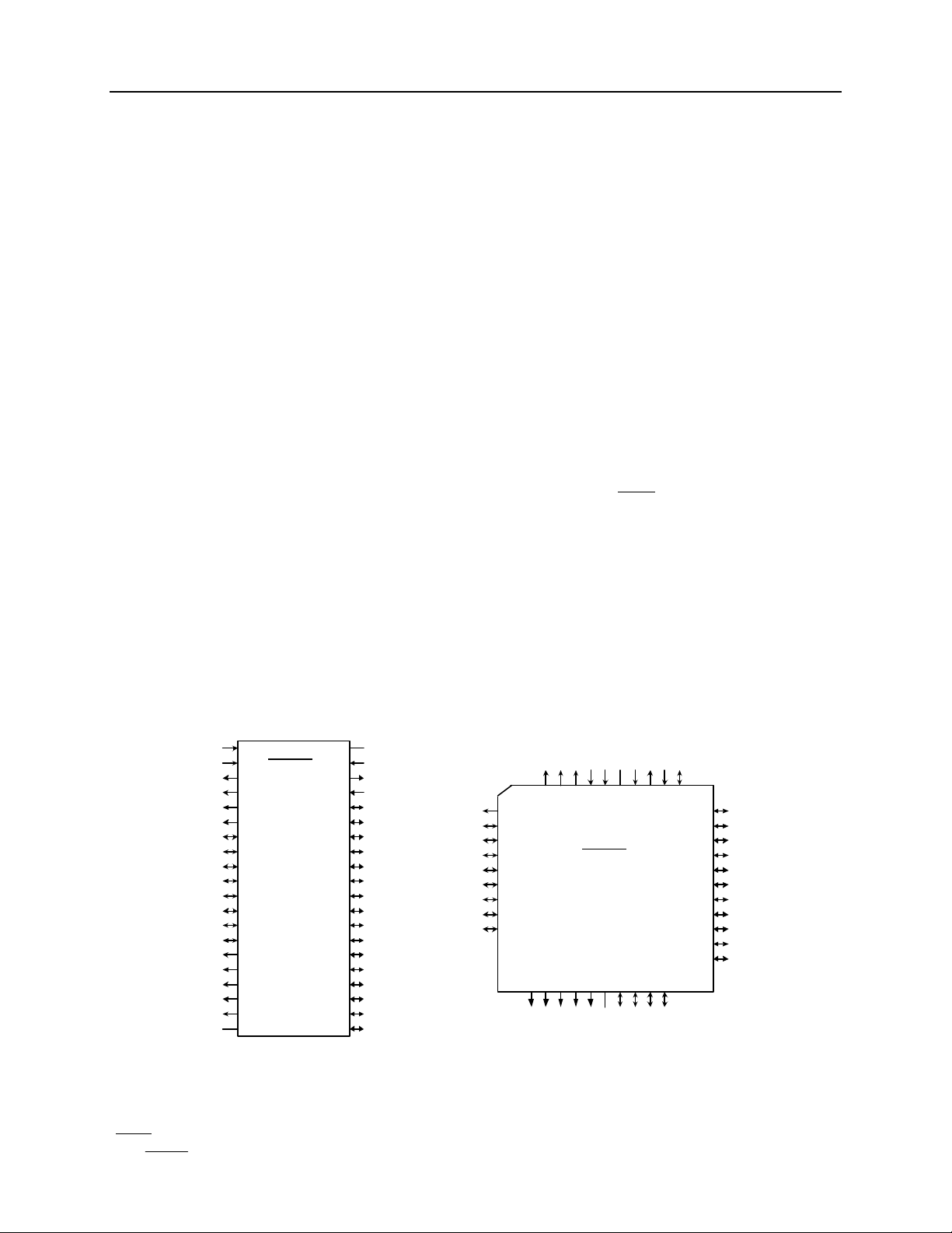
Package Pinout
IRQ_N
PA6
PA4
PA3
PA0
A10
(1)RESET_N
IA6805E2
(2)
40 Pin DIP
(3)
LI
(4)DS
(5)RW_N
(6)AS
(7)PA7
(8)
(9)PA5
(10)
(11)
(12)PA2
(13)PA1
(14)
(15)A12
(16)A11
(17)
(18)A9
(19)A8
(20)VSS
(40)
(39)
(38)
(37)
(36)
(35)
(34)
(33)
(32)
(31)
(30)
(29)
(28)
(27)
(26)
(25)
(24)
(23)
(22)
(21)
VDD
OSC1
OSC2
TIMER
PB0
PB1
PB2
PB3
PB4
PB5
PB6
PB7
B0
B1
B2
B3
B4
B5
B6
B7
PA6
RW_N
NC
DS
(6)
(5)
(18)
A12
(19)
A11
(4)
(20)
A10
(7)AS
(8)PA7
(9)
(10)PA5
(11)PA4
(12)PA3
(13)PA2
(14)PA1
(15)PA0
(16)NC
(17)NC
IRQ_N
RESET_N
LI
(3)
(2)
(1)
IA6805E2
44 Pin LCC
(21)
(22)
(23)
A8A9B7
VSS
VDD
(44)
(24)
OSC1
(43)
(25)
(42) OSC2
(26)
B5B6B4
PB0
(41) TIMER
(27)
(40)
(28)
NC
(39)
(38)
(37)
(36)
(35)
(34)
(33)
(32)
(31)
(30)
(29)
PB1
PB2
PB3
PB4
PB5
PB6
PB7
B0
B1
B2
B3
Copyright 2002 ENG21108140100 www.innovasic.com
innovASIC Customer Support:
The End of Obsolescence Page 1 of 31 1-888-824-4184
Page 2
IA6805E2 Data Sheet
Microprocessor Unit As of Production Version 00
Description
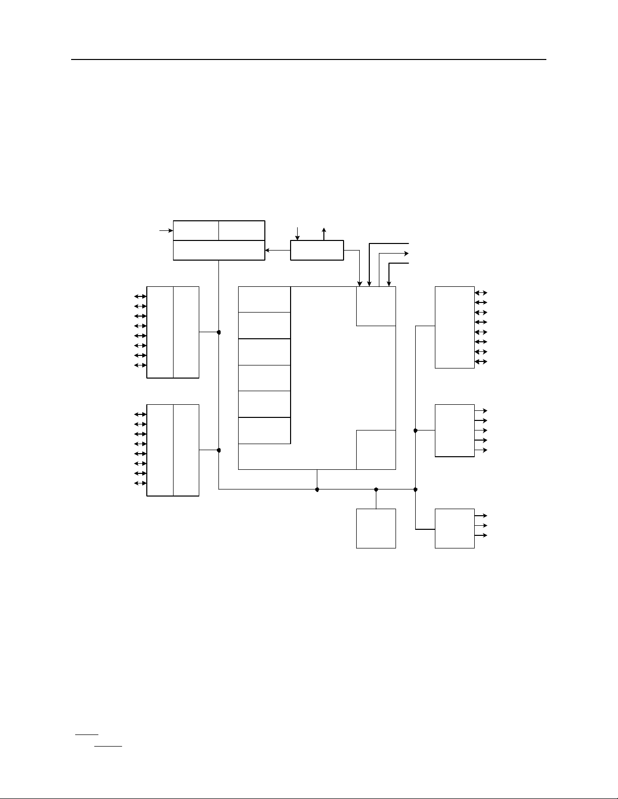
The IA6805E2 (CMOS) Microprocessor Unit (MPU) is a low cost, low power MPU. It features a
CPU, on-chip RAM, parallel I/O compatibility with pins programmable as input or output. The
following paragraphs will further describe this system block diagram and design in more detail.
PORT
A
I/O
LINES
PORT
B
I/O
LINES
PA0
PA1
PA2
PA3
PA4
PA5
PA6
PA7
PB0
PB1
PB2
PB3
PB4
PB5
PB6
PB7
TIMER
PA0
PORT
A
REG
PORT
B
REG
PRESCALER
TIMER CONTROL
DATA
DIR
REG
DATA
DIR
REG
TIMER/
COUNTER
ACCUMULATOR
8 A
REGISTER
8
CONDITION
REGISTER
5
POINTER
6
PROGRAM
COUNTER
5
PROGRAM
COUNTER
8
INDEX
CODE
STACK
HIGH
LOW
OSC1 OSC2
OSCILLATOR
X
CC
SP
PCH
PCL
CPU
RESET_N
CPU
CONTROL
ALU
112x8
RAM
IRQ_N
LI
B0
B1
B2
MUX
BUS
DRIVE
ADDRESS
DRIVE
BUS
CONTROL
B3
B4
B5
B6
B7
A8
A9
A10
A11
A12
AS
DS
RW_N
MULTIPLEXED
ADDRESS
DATA
BUS
ADDRESS
BUS
ADDRESS STROBE
DATA STROBE
READ/WRITE
Figure 1. System Block Diagram
Copyright 2002 ENG21108140100 www.innovasic.com
innovASIC Customer Support:
The End of Obsolescence Page 2 of 31 1-888-824-4184
Page 3
IA6805E2 Data Sheet
SS
RESET_n
IRQ_n
LI
DS
RW_n
AS
PA0-PA7/PB0-PB7
.
A8-A12
B0-B7
OSC1, OSC2
Microprocessor Unit As of Production Version 00
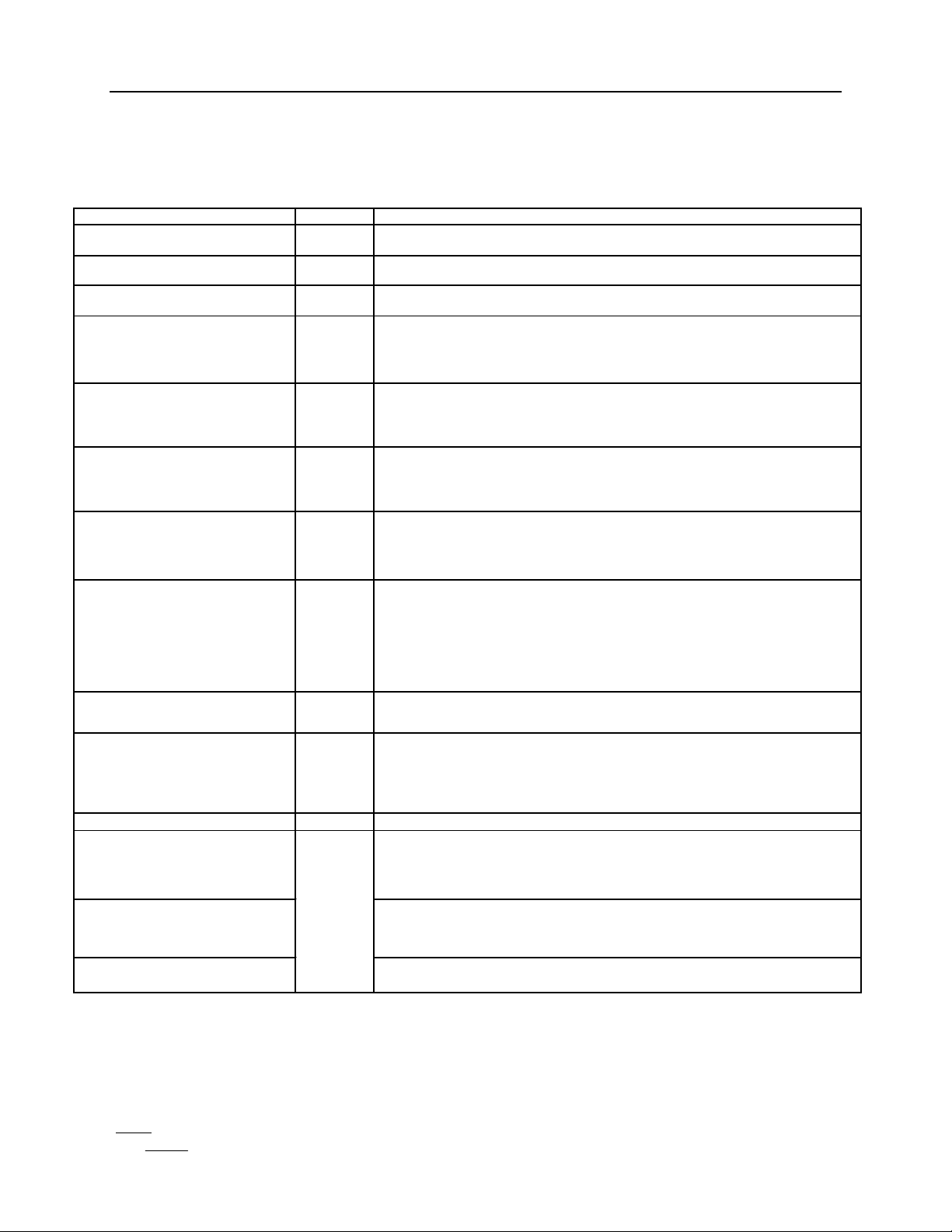
I/O Signal Description
The table below describes the I/O characteristics for each signal on the IC. The signal names
correspond to the signal names on the pinout diagrams provided.
SIGNAL NAME I/O
VDD and V
(Power and Ground)
(Reset)
(Interrupt Request)
(Load Instruction)
(Data Strobe)
(Read/Write)
(Address Strobe)
(Input/Output Lines)
N/A
I
I
O
O
O
O
I/O
DESCRIPTION
Source: These two pins provide power to the chip. VDDprovides +5 volts (±0.5) power
and VSS is ground.
TTL:Input pin that can be used to reset the MPU's internal state by pulling the reset_n
pin low.
TTL: Input pin that is level and edge sensitive. Can be used to request an interrupt
sequence.
TTL with slew rate control: Output pin used to indicate that a next opcode fetch is in
progress. Used only for certain debugging and test systems. Not connected in normal
operation. Overlaps Data Strobe (DS) signal. This output is capable of driving one
standard TTL load and 50pF.
TTL with slew rate control: Output pin used to transfer data to or from a peripheral or
memory. DS occurs anytime the MPU does a data read or write and during data transfer
to or from internal memory. DS is available at f
or STOP mode. This output is capable of driving one standard TTL load and 130pF.
TTL with slew rate control: Output pin used to indicate the direction of data transfer
from internal memory, I/O registers, and external peripheral devices and memories.
Indicates to a selected peripheral whether the MPU is to read (RW_n high) or write
(RW_n low) data on the next data strobe. This output is capable of driving one standard
TTL load and 130pF.
TTL with slew rate control: Output strobe used to indicate the presence of an address
on the 8-bit multiplexed bus. The AS line is used to demultiplex the eight least significant
address bits from the data bus. AS is available at f
WAIT or STOP modes. This output is capable of driving one standard TTL load and
130pF.
TTL with slew rate control: These 16 lines constitute Input/Output ports A and B.
Each line is individually programmed to be either an input or output under software
control of the Data Direction Register (DDR) as shown below in Table 1 and Figure 2
The port I/O is programmed by writing the corresponding bit in the DDR to a "1" for
output and a "0" for input. In the output mode the bits are latched and appear on the
corresponding output pins. All the DDR's are initialized to a "0" on reset. The output
port registers are not initialized on reset. Each output is capable of driving one standard
TTL load and 50pF.
÷ 5 when the MPU is not in the WAIT
OSC
÷ 5 when the MPU is not in the
OSC
TTL with slew rate control: These five outputs constitute the higher order nonmultiplexed address lines. Each output is capable of driving one standard TTL load and
(High Order Address Lines)
(Address/Data Bus)
Timer I
(System Clock)
Crystal
External Clock
O
I/O
I/O
130pF.
TTL with slew rate control: These bi-directional lines constitute the lower order
addresses and data. These lines are multiplexed with address present at address strobe
time and data present at data strobe time. When in the data mode, these lines are bidirectional, transferring data to and from memory and peripheral devices as indicated by
the RW_n pin. As outputs,these lines are capable of driving one standard TTL load and
130pF.
TTL: Input used to control the internal timer/counter circuitry.
TTL Oscillator input/output: These pins provide control input for the on-chip clock
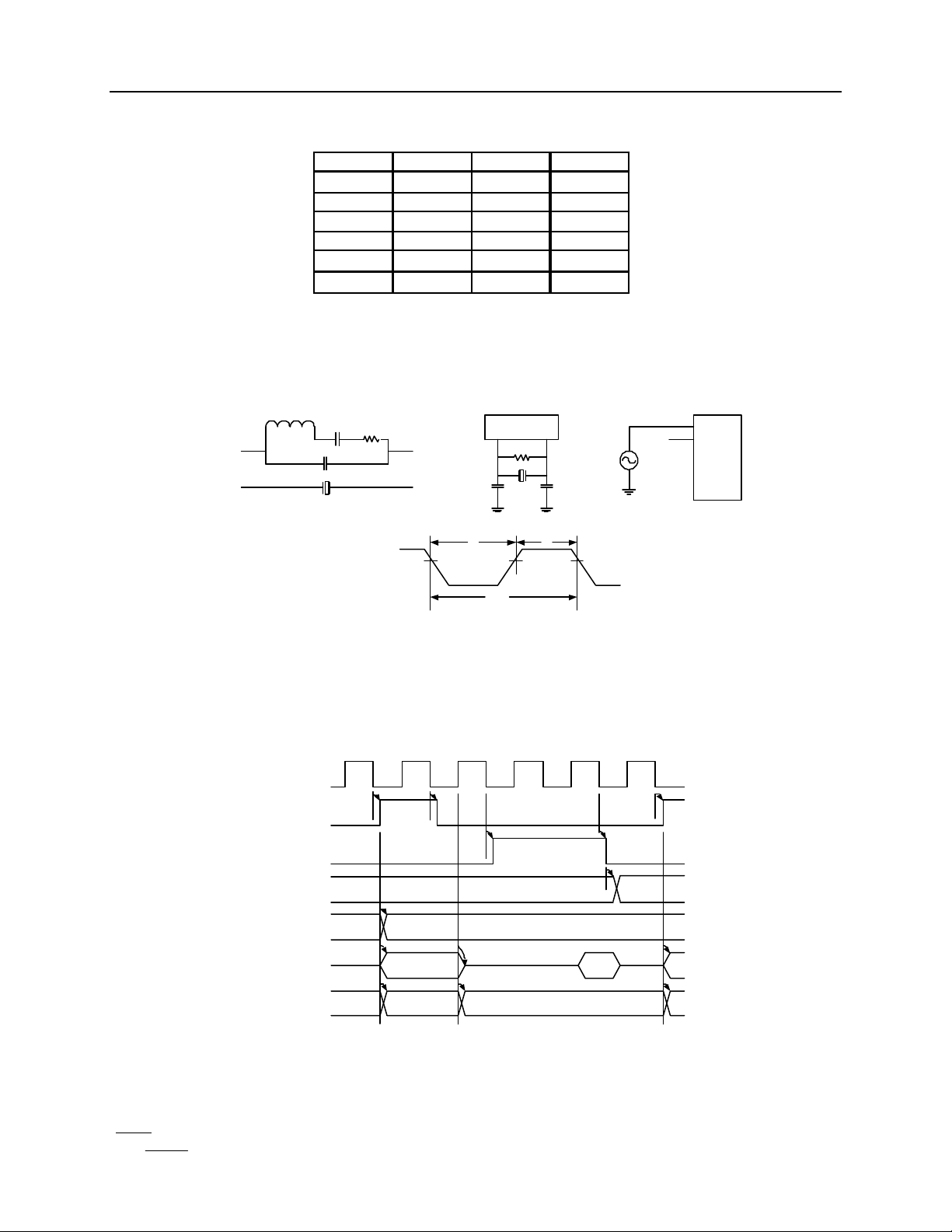
oscillator circuits. Either a crystal or external clock is connected to these pins to provide
a system clock. The crystal connection is shown in Figure 3 . The OSC1 to bus
transitions for system designs using oscillators slower than 5MHz is shown in Figure 4 .
The circuit shown in Figure 3 is recommended when using a crystal. An external CMOS
oscillator is recommended when using crystals outside the specified ranges. To minimize
output distortion and start-up stabilization time, the crystal and components should be
mounted as close to the input pins as possible.
When an external clock is used, it should be applied to the OSC1 input with the OSC2
input not connected, as shown in Figure 3 .
Copyright 2002 ENG21108140100 www.innovasic.com
innovASIC Customer Support:
The End of Obsolescence Page 3 of 31 1-888-824-4184
Table 1
Page 4
IA6805E2 Data Sheet
Microprocessor Unit As of Production Version 00
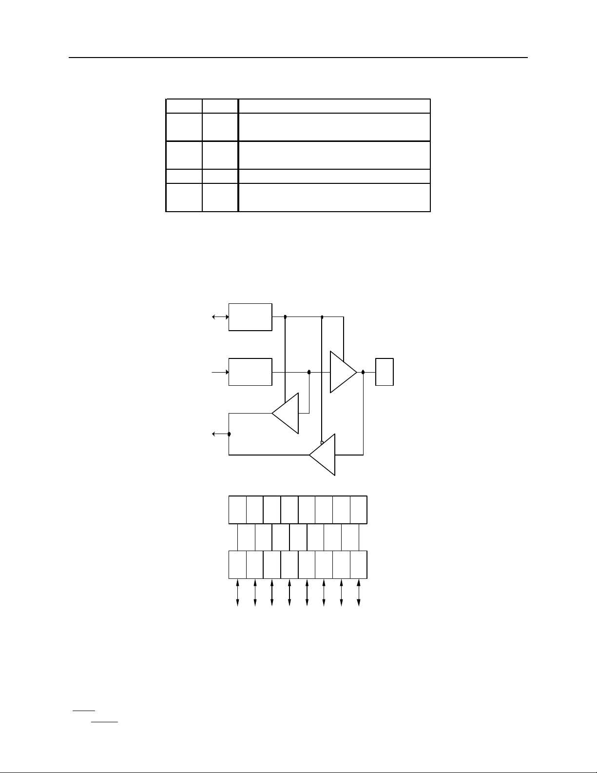
I/O Pin Functions
R/W-n DDR I/O Pin Functions
0 0
0 1
1 0
1 1
I/O Port Circuitry and Register Configuration:
TO
The I/O pin is in input mode. Data is
written into the output data latch.
Data is written into the output data latch and
output to the I/O pin.
The state of the I/O pin is read.
the I/O pin is in an output mode. The
output data latch is read.
DATA DIRECTION
REGISTER
BIT
AND
FROM
CPU
DATA DIRECTION
A(B)
REGISTER
PORT A(B)
REGISTER
LATCHED
OUTPUT
DATA BIT
7 456 3 012
PIN
DDA7
(DDB7)
PA7
(PB7)
DDA6
(DDB6)
PA6
(PB6)
DDA5
(DDB5)
PA5
(PB5)
INPUT
REG
BIT
DDA4
(DDB4)
PA4
(PB4)
DDA3
(DDB3)
PA3
(PB3)
INPUT
I/O
PIN
DDA2
(DDB2)
PA2
(PB2)
OUTPUT
DDA1
(DDB1)
PA1
(PB1)
DDA0
(DDB0)
PA0
(PB0)
I/O
PIN
$0004 ($0005)
$0000 ($0001)
Figure 2. PA0-PA7/PB0-PB7 (Input/Output Lines)
Copyright 2002 ENG21108140100 www.innovasic.com
innovASIC Customer Support:
The End of Obsolescence Page 4 of 31 1-888-824-4184
Page 5
IA6805E2 Data Sheet
Ω75Ω
Ω
OSC1
OSC2
Figure 3. OSC1, OSC2 (System Clock)
Microprocessor Unit As of Production Version 00
Crystal Parameters Representative Frequencies:
5.0 MHz 4.0 MHz 1.0 MHz
RS max 50
C0 8 pF 7 pF 5 pF
C1 0.02 pF 0.012 pF 0.008 pF
Q 50 k 40 k 30 k
C
C
Oscillator Connections:
CRYSTAL CIRCUIT CRYSTAL OSCILLATOR CONNECTIONS
L
C1
38
38
OSC2
C0
15-30 pF 15-30 pF 15-40 pF
15-25 pF 15-25 pF 15-30 pF
RS
39
OSC1OSC2
39
OSC1
ia6805E2
38 39
OSC2 OSC1
C
10 M
OSC2
400
OSC1
39
OSC2
38
Ω
C
OSC1
NC
IA6805E2
t
OSC1 PIN
OL
t
t
OLOL
OSC1 to Bus Transitions Timing Waveforms:
OSC1
AS
DS
RW_n
A[12:8]
B[7:0]
MPU READ
B[7:0]
MPU WRITE
*READ DATA "LATCHED" ON DS FALL
MUX ADDR
MUX ADDR MPU WRITE DATA
t
OH
MPU
READ
DATA*
Figure 4. OSC1, OSC2 (System Clock)
Copyright 2002 ENG21108140100 www.innovasic.com
innovASIC Customer Support:
The End of Obsolescence Page 5 of 31 1-888-824-4184
Page 6

IA6805E2 Data Sheet
Microprocessor Unit As of Production Version 00
Functional Description
Memory:
The MPU is capable of addressing 8192 bytes of memory and I/O registers. The locations
are divided into internal memory space and external memory space as shown in Figure 5.
The first 128 bytes of memory contain internal port I/O locations, timer locations, and 112
bytes of RAM. The MPU can read from or write to any of these locations. During program
reads from on chip locations, the MPU accepts data only from the addressed on chip
location. Any read data appearing on the input bus is ignored. The shared stack area is used
during interrupts or subroutine calls. A maximum of 64 bytes of RAM is available for stack
usage. The stack pointer is set to $7f at power up. The unused bytes of the stack can be used
for data storage or temporary work locations, but care must be taken to prevent it from
being overwritten due to stacking from an interrupt or subroutine call.
ACCESS VIA
PAGE 0
DIRECT
ADDRESS
INTERRUPT
VECTORS
0
I/O PORTS
TIMER RAM
127
128
255
256
EXTERNAL MEMORY
SPACE (8064 BYTES)
TIMER INTERRUPT FROM WAIT STATE ONLY
TIMER INTERRUPT
EXTERNAL INTERRUPT
SWI
8191
RESET
$0000
$007F
$0080
$00FF
$0100
$1FF6 - $1FF7
$1FF8 - $1FF9
$1FFA - $1FFB
$1FFC - $1FFD
$1FFE - $1FFF
0
1
2
3
4
5
6
7
8
9
10
15
16
63
64
127
PORT A DATA REGISTER
PORT B DATA REGISTER
EXTERNAL MEMORY SPACE
EXTERNAL MEMORY SPACE
PORT A DATA DIRECTION REGISTER
PORT B DATA DIRECTION REGISTER
EXTERNAL MEMORY SPACE
EXTERNAL MEMORY SPACE
TIMER DATA REGISTER
TIMER CONTROL REGISTER
EXTERNAL MEMORY SPACE
(112 BYTES)
RAM
STACK
(64 BYTES MAX)
Figure 5. Memory Map
Copyright 2002 ENG21108140100 www.innovasic.com
innovASIC Customer Support:
The End of Obsolescence Page 6 of 31 1-888-824-4184
Page 7
IA6805E2 Data Sheet
Figure 6. Programming Model
Microprocessor Unit As of Production Version 00
Registers:
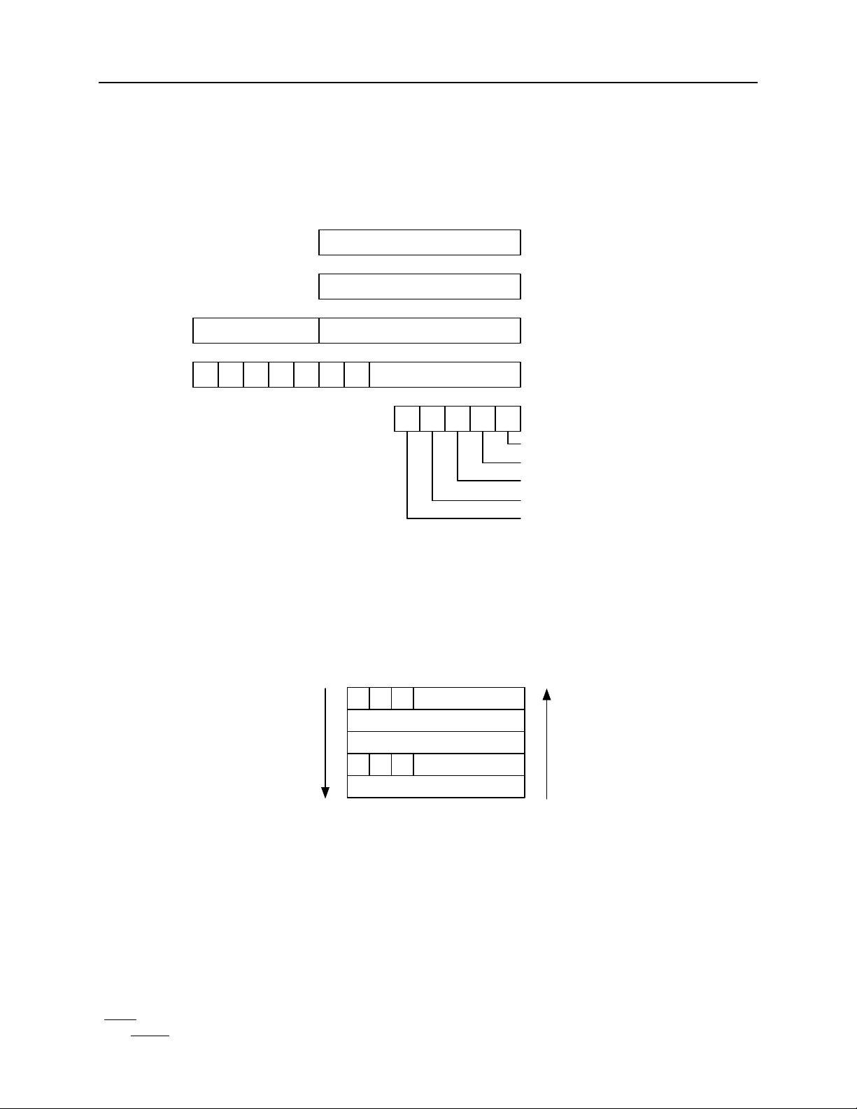
The following paragraphs describe the registers contained in the MPU. Figure 6 shows the
programming model an d Figure 7 shows the interrupt stacking order.
7 0
A
7 0
X
12 078
PCH
12 6 0
PCL
SP10 0 0 0 0 0
4
H I N Z C
CC
ACCUMULATOR
INDEX REGISTER
PROGRAM COUNTER
STACK POINTER
0
CONDITION CODE REGISTER
CARRY/BORROW
ZERO
NEGATIVE
INTERRUPT MASK
HALF CARRY
NOTE: Since the stack pointer decrements during pushes, the PCL is stacked first,
followed by PCH, etc. Pulling from the stack is in the reverse order.
STACK
INCREASING MEMORY
ADDRESSES
UNSTACK
CONDITION CODE
R
E
T
U
R
N
111
ACCUMULATOR
INDEX REGISTER
REGISTER
PCH000
PCL
I
N
T
E
R
R
U
P
T
DECREASING MEMORY
ADDRESSES
Figure 7. Interrupt Stacking Order
Copyright 2002 ENG21108140100 www.innovasic.com
innovASIC Customer Support:
The End of Obsolescence Page 7 of 31 1-888-824-4184
Page 8

IA6805E2 Data Sheet
Microprocessor Unit As of Production Version 00
A(Accumulator):
The accumulator is an 8-bit register used to hold operands and results of arithmetic
calculations or data manipulations.
X(Index Register):
The index register is an 8-bit register used during the indexed addressing mode. It contains
an 8-bit value used to create an effective address. The index register may also be used as a
temporary storage area when not performing addressing operations.
PC(Program Counter):
The program counter is a 13-bit register that holds the address of the next instruction to be
performed by the MPU.
SP(Stack Pointer):
The stack pointer is a 13-bit register that holds the address of the next free location on the
stack. During an MPU reset or the reset stack pointer (RSP) instruction, the stack pointer is
set to location $007f. The seven most significant bits of the stack pointer are permanently
set to 0000001. They are appended to the six least significant register bits to produce an
address range down to location $0040. The stack pointer gets decremented as data is pushed
onto the stack and incremented as data is removed from the stack. The stack area of RAM is
used to store the return address on subroutine calls and the machine state during interrupts.
The maximum number of locations for the stack pointer is 64 bytes. If the stack goes
beyond this limit the st ack pointer wraps around and points to its upper limit thereby losing
the previously stored information. Subroutine calls use 2 bytes of RAM on the stack and
interrupts use 5 bytes.
CC(Condition code Register):
The condition code register is a 5-bit register that indicates the results of the instruction just
executed. The bit is set if it is high. A program can individually test these bits and specific
actions can be taken as a result of their states. Following is an explanation of each bit.
C(Carry Bit):
The carry bit indicates that a carry or borrow out of the Arithmetic Logical Unit (ALU)
occurred during the last arithmetic instruction. This bit is also modified during bit test, shift,
rotate, and branch types of instructions.
Z(Zero Bit):
The zero bit indicates the result of the last arithmetic, logical, or data manipulation was zero.
N(Negative Bit):
The negative bit indicates the result to the last arithmetic, logical, or data manipulation was
negative (bit 7 in the result is high).
Copyright 2002 ENG21108140100 www.innovasic.com
innovASIC Customer Support:
The End of Obsolescence Page 8 of 31 1-888-824-4184
Page 9

IA6805E2 Data Sheet
Microprocessor Unit As of Production Version 00
I(Interrupt Mask Bit)
The interrupt mask bit indicates that both the external interrupt and the timer interrupt are
disabled (masked). If an interrupt occurs while this bit is set, the interrupt is latched and is
processed as soon as the interrupt bit is cleared.
H(Half Carry Bit)
The half carry bit indicates that a carry occurred between bits 3 and 4 of the ALU during an
ADD or ADC operation.
Resets:
The MPU can be reset by initial power up or by the external reset pin (reset_n).
POR(Power On Reset)
Power on reset occurs on initial power up. It is strictly for power initialization conditions
and should not be used to detect drops in the power supply voltage. There is a 1920 t
time out delay from the time the oscillator is detected. If the reset_n pin is still low at the
end of the delay, the MPU will remain in the reset state until the external pin goes high.
CYC
Reset_n
The reset_n pin is used to reset the MPU. The reset pin must stay low for a minimum of t
to guarantee a reset. The reset_n pin is provided with a Schmitt Trigger to improve noise
immunity capability.
Interrupts:
The MPU can be interrupted with the external interrupt pin (irq_n), the internal timer
interrupt request, or the software interrupt instruction. When any of these interrupts occur,
normal processing is suspended at the end of the current instruction execution. The
processor registers are saved on the stack (stacking order shown in Figure 7) and the
interrupt mask (I) is set to prevent additional interrupts. Normal processing resumes after
the RTI instruction causes the register contents to be recovered from the stack. When the
current instruction is completed, the processor checks all pending hardware interrupts and if
unmasked (I bit clear) proceeds with interrupt processing. Otherwise, the next instruction is
fetched and executed. Masked interrupts are latched for later interrupt service. External
interrupts hold higher priority than timer interrupts. At the end of an instruction execution,
if both an external interrupt and timer interrupt are pending, the external interrupt is
serviced first. The SWI gets executed with the same priority as any other instruction if the
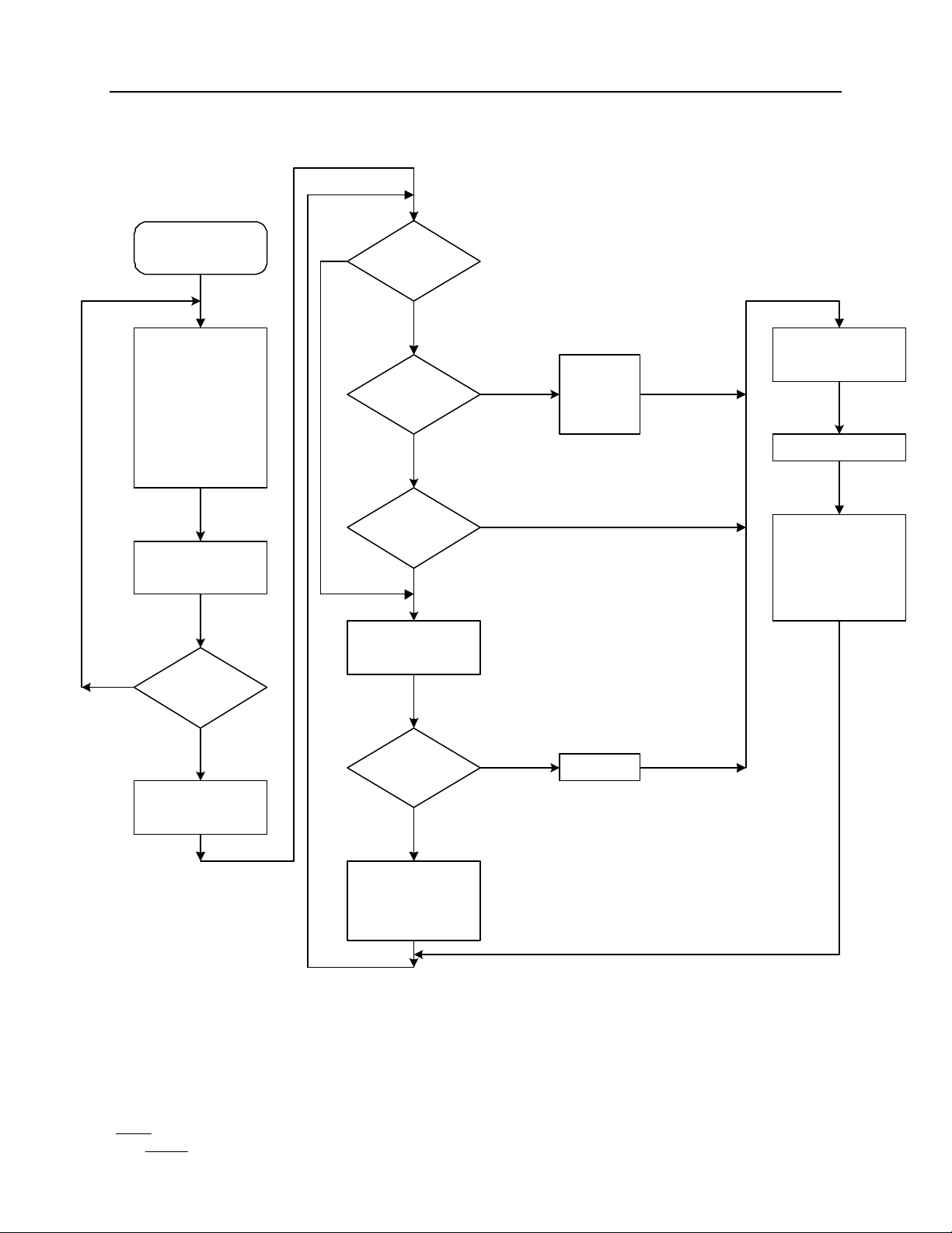
hardware interrupts are masked (I bit set). Figure 8 shows the Reset and Interrupt processing
flowchart.
cyc
Copyright 2002 ENG21108140100 www.innovasic.com
innovASIC Customer Support:
The End of Obsolescence Page 9 of 31 1-888-824-4184
Page 10
IA6805E2 Data Sheet
Figure 8. Reset and Interrupt Processing Flowchart
Microprocessor Unit As of Production Version 00
RESET_N
PIN = LOW
RESET
I_CC <= 1
SP <= $007F
DDRs <= 0
CLR IRQ_N LOGIC
TIMER <= $FF
PRESCALER <= $7F
TCR <= $7f
PUT 1FFE,1FFF ON
ADDRESS BUS
Y
RESET
N
LOAD PC
FROM
1FFE/1FFF
IN
?
RESET_N
PIN = LOW
SET
I BIT
?
CLEAR
IRQ_N
EDGE
?
N
TCR6=0
AND
TCR7=1?
N
FETCH
INSTRUCTION
IS FETCHED
INSTRUCTION
AN SWI?
N
STACK
CLEAR
IRQ_N
REQUEST
LATCH
Y
Y
PC+1=>PC
IRQ_NY
TIMER
SWI
PC, X, A, CC
I <= 1
LOAD PC FROM:
SWI: 1FFC/1FFD
IRQ_N: 1FFA/1FFB
TIMER: 1FF8/1FF9
TIMER WAIT:1FF6/
1FF7
EXECUTE ALL
INSTRUCTION
CYCLES
Copyright 2002 ENG21108140100 www.innovasic.com
innovASIC Customer Support:
The End of Obsolescence Page 10 of 31 1-888-824-4184
Page 11

IA6805E2 Data Sheet
Figure 9. Interrupt Functional Diagram
Microprocessor Unit As of Production Version 00
External Interrupt:
If the external interrupt pin irq_n is “low” and the interrupt mask bit of the condition code
register is cleared, the external interrupt occurs. When the interrupt is recognized, the
current state of the machine is pushed onto the stack and the condition code register I-bit
gets set masking further interrupts until the present one is serviced. The program counter is
then loaded with the contents of the interrupt vector, which contains the location of the
interrupt service routine. The contents of $1FFA and $1FFB specify the address for this
service routine. A functional diagram of the external interrupt is shown in Figure 9 and a
mode diagram of the external interrupt is shown in Figure 10. The timing diagram shows
two different treatments of the interrupt line (irq_n) to the processor. The first shows
several interrupt lines “wire ORed” to form the interrupts at the processor. If the interrupt
line (irq_n) remains low after servicing an interrupt, the next interrupt is recognized. The
second shows single pulses on the interrupt line spaced far enough apart to be serviced. The
minimum time between pulses is a function of the length of the interrupt service. After a
pulse occurs, the next pulse should not occur until an RTI has occurred. The time be tween
pulses (t
to complete the service routine including the RTI instruction.
) is obtained by adding 20 instruction cycles to the total number of cycles it takes
ILIL
INTERRUPT PIN
VDD
DCQ
R
Q
I BIT (CCR)
POWER-ON RESET
EXTERNAL RESET
EXTERNAL INTERRUPT
BEING SERVICED
EXTERNAL
INTERUPT
REQUEST
Copyright 2002 ENG21108140100 www.innovasic.com
innovASIC Customer Support:
The End of Obsolescence Page 11 of 31 1-888-824-4184
Page 12

IA6805E2 Data Sheet
Microprocessor Unit As of Production Version 00
Timer Interrupt:
If the timer mask bit (TCR6) and the interrupt mask bit (I) of the condition code register are
cleared, each time the timer decrements to zero ($01 to $00 transition) an interrupt request is
generated. When the interrupt is recognized, the current state of the machine is pushed onto
the stack and the condition code register I-bit gets set masking further interrupts until the
present one is serviced. The program counter is then loaded with the contents of the timer
interrupt vector, which contains the location of the timer interrupt service routine. The
contents of $1FF8 and $1FF9 specify the address for this service routine. If the MPU is in
the wait mode and a timer interrupt occurs, then the contents of $1FF6 and $1FF7 specify
the service routine. When the timer interrupt service routine is complete, the software
executes an RTI instruction to restore the machine state and starts executing the interrupt
program.
Software Interrupt:
Software interrupt is an executable instruction regardless of the state of the interrupt mask
bit (I) in the condition code regis ter. SWI is similar to hardware interrupts. It executes after
the other interrupts if the interrupt mask bit is zero. The contents of $1FFC and $1FFD
specify the address for this service routine.
Figure 10. Interrupt Mode Diagram
Low Power Modes:
The low power modes consist of the stop instruction and the wait instruction. The
following paragraphs explain these modes of operation.
Copyright 2002 ENG21108140100 www.innovasic.com
innovASIC Customer Support:
The End of Obsolescence Page 12 of 31 1-888-824-4184
Page 13

IA6805E2 Data Sheet
Microprocessor Unit As of Production Version 00
Stop Modes:
The stop instruction places the MPU in low power consumption mode. The stop instruction
disables clocking of most internal registers. Timer control register bits 6 and 7 (TCR6 and
TCR7) are altered to remove any pending timer interrupt requests and to disable any further
timer interrupts. The DS and AS output lines go “low” and the RW_n line goes “high”. The
multiplexed address/data bus goes to the data input state. The high order address lines
remain at the address of the next instruction. External interrupts are enabled by clearing the
I bit in the condition code register. All other registers, memory, and I/O remain unaltered.
Only an external interrupt or reset will bring the MPU out of the stop mode. Figure 11
shows a flowchart of the stop function.
STOP
TCR BIT 7 <= 0
TCR BIT 6 <= 1
CLEAR I BIT
N
N
EXTERNAL
INTERRUPT?
Y
RESET?
Y
FETCH EXTERNAL
INTERRUPT
OR RESET VECTOR
Figure 11. STOP Function Flowchart
Copyright 2002 ENG21108140100 www.innovasic.com
innovASIC Customer Support:
The End of Obsolescence Page 13 of 31 1-888-824-4184
Page 14

IA6805E2 Data Sheet
Microprocessor Unit As of Production Version 00
Wait Mode:
The wait instruction places the MPU in low power consumption mode. The wait instruction
disables clocking of most internal registers. The DS and AS output lines go “low” and the
RW_n line goes “high”. The multiplexed address/data bus goes to the data input state. The
high order address lines remain at the address of the next instruction. External interrupts are
enabled by clearing the I bit in the condition code register. All other registers, memory, and
I/O remain unaltered. Only an external interrupt, timer interrupt, or reset will bring the
MPU out of the wait mode. The timer may be enabled to allow a periodic exit from the wait
mode. If an external and a timer interrupt occur at the same time, the external interrupt is
serviced first. Then, if the timer interrupt request is not cleared in the external interrupt
routine, the normal timer interrupt (not the timer wait interrupt) is serviced since the MPU is
no longer in the wait mode. Figure 12 shows a flowchart of the wait function.
WAIT
OSCILLATOR
ACTIVE,
CLEAR I BIT,
TIMER CLOCK
ACTIVE,
RESET?
Y
FETCH EXTERNAL
INTERRUPT, RESET,
OR TIMER
INTERRUPT (FROM
WAIT MODE ONLY)
N
EXTERNAL
INTERRUPT?
Y
N
TIMER
INTERRUPT?
(TCR BIT7
= 1)
Y
TCR
BIT 6 = 0?
Y
N
N
Copyright 2002 ENG21108140100 www.innovasic.com
innovASIC Customer Support:
The End of Obsolescence Page 14 of 31 1-888-824-4184
Figure 12. WAIT Function Flowchart
Page 15

IA6805E2 Data Sheet
Microprocessor Unit As of Production Version 00
Timer:
The MPU contains a single 8-bit software programmable counter driven by a 7-bit software
programmable prescaler. The counter may be loaded under program control and decrements
to zero. When the counter decrements to zero, the timer interrupt request bit in the timer
control register (TCR7) is set. Figure 13 shows a block diagram of the timer. If the timer
mask bit (TCR6) and the interrupt mas k bit (I) of the condition code register are cleared, an
interrupt request is generated. After completion of the current instruction, the current state
of the machine is pushed onto the stack. The timer interrupt vector address is then fetched
from locations $1FF8 and $1FF9 and the interrupt routine is executed, unless the MPU was
in the WAIT mode in which case the interrupt vector address in locations $1FF6 and $1FF7
is fetched. Power-On-Reset causes the counter to set to $FF.
NOTE: 1. Prescaler and counter are clocked on the falling edge of the internal
clock (AS) or external input.
2. Counter is written to during Data Strobe (DS) and counts down continuously.
TIMER
(PIN 37)
INTERNAL
CLOCK
TIMER_n
ENABLE /
DISABLE_n
INTERNAL_n / EXTERNAL
TCR4 TCR5 TCR3 TCR2 TCR1 TCR0
EXT
CLK
INT
CLK
2 - TO - 1
MUX
PRESCALER
(7 BITS)
SETTING TCR3 CLEARS
PRESCALER TO ÷ 1
SOFTWARE FUNCTIONS
COUNTER
(8 BITS)
INTERRUPT
CONTROL
INTERRUPT
WRITEREAD
Figure 13. Timer Block Diagram
Copyright 2002 ENG21108140100 www.innovasic.com
innovASIC Customer Support:
The End of Obsolescence Page 15 of 31 1-888-824-4184
Page 16

IA6805E2 Data Sheet
Microprocessor Unit As of Production Version 00
The counter continues to count past zero, falling from $00 to $FF, and continues. The
processor may read the counter at any time without disturbing the count by reading the
timer data register (TDR). This allows a program to determine the length of time since a
timer interrupt has occurred. The timer interrupt request bit remains set until cleared by
software. The interrupt is lost if this happens before the timer interrupt is serviced.
The prescaler is a 7-bit divider used to extend the maximum length of the timer. TCR bits
0-2 are programmed to choose the appropriate prescaler output, which is used as the count
input. The prescaler is cleared by writing a “1” into TCR bit 3, which avoids truncation
errors. The processor cannot write to or read from the prescaler.
Timer Input Mode 1:
When TCR4 = 0 and TCR5 = 0, the input to the timer is from an internal clock and the
timer input is disabled. The internal clock mode can be used for periodic interrupt
generation as well as a reference for frequency and event measurement. The internal clock is
the instruction cycle clock and is coincident with Address Strobe (AS) except during the wait
instruction where it goes low. During the wait instruction the internal clock to the timer
continues to run at its normal rate.
Timer Input Mode 2:
When TCR4 = 1 and TCR5 = 0, the internal clock and timer input signal are ANDed to
form the timer input. This mode can be used to measure external pulse widths. The external
pulse turns on the internal clock for the duration of the pulse. The count accuracy in this
mode is ±1 clock. Accuracy improves with longer input pulse widths.
Timer Input Mode 3:
When TCR4 = 0 and TCR5 = 1, all inputs to the timer are disabled.
Timer Input Mode 4:
When TCR4 = 1 and TCR5 = 1, the internal clock input to the timer is disabled and the
timer input then comes from the external TIMER pin. The external clock can be used to
count external events as well as to provide an external frequency for generating periodic
interrupts.
Copyright 2002 ENG21108140100 www.innovasic.com
innovASIC Customer Support:
The End of Obsolescence Page 16 of 31 1-888-824-4184
Page 17

IA6805E2 Data Sheet
Microprocessor Unit As of Production Version 00
TCR (Timer Control Register ($0009)):
An 8-bit register that controls functions such as configuring operation mode, setting ratio of
the prescaler, and generating timer interrupt request signals. All bits except bit 3 are
read/write. Bits TCR5 - TCR0 are unaffected by reset_n.
7 6 5 4 3 2 1 0
TCR7 TCR6 TCR5 TCR4 TCR3 TCR2 TCR1 TCR0
Reset:
0 1 0 0 0 0 0 0
TCR7 – Timer Interrupt Request
Used to indicate the timer interrupt when it is logic one.
1 – Set when the counter decrements to zero or under program control.
0 – Cleared on external reset, POR, STOP instruction, or program control.
TCR6 – Timer Interrupt Mask
Used to inhibit the timer interrupt.
1 – Interrupt inhibited. Set on external reset, POR, STOP instruction, or program
control.
0 – Interrupt enabled.
TCR5 – External or Internal
Selects input clock source. Unaffected by reset.
1 – External clock selected.
0 – Internal clock selected (AS) (f
OSC
/5).
TCR4 – Timer External Enable
Used to enable external timer pin or to enable the internal clock. Unaffected by reset.
1 – Enables external timer pin.
0 – Disables external timer pin.
Copyright 2002 ENG21108140100 www.innovasic.com
innovASIC Customer Support:
The End of Obsolescence Page 17 of 31 1-888-824-4184
Page 18

IA6805E2 Data Sheet
÷
÷
÷
÷
÷
÷
÷
÷
Microprocessor Unit As of Production Version 00
TCR3 – Prescaler Clear
Write only bit. Writing a “1” to this bit resets the prescaler to zero. A read of this location
always indicates a zero. Unaffected by reset.
TCR2, TCR1, TCR0 – Prescaler select bits
Decoded to select one of eight outputs of the prescaler. Unaffected by reset.
Prescaler
TRC2 TRC1 TRC0 RESET
0 0 0
0 0 1
1
2
0 1 0
0 1 1
1 0 0
1 0 1
1 1 0
1 1 1
4
8
16
32
64
128
Copyright 2002 ENG21108140100 www.innovasic.com
innovASIC Customer Support:
The End of Obsolescence Page 18 of 31 1-888-824-4184
Page 19

IA6805E2 Data Sheet
Microprocessor Unit As of Production Version 00
Instruction Set Description
The MPU has 61 basic instructions divided into 5 types. The 5 types are Register/memory, readmodify-write, branch, bit manipulation, and control.
Register/Memory Instructions:
Most of the following instructions use two operands. One is either the accumulator or the
index register and the other is obtained from memory. The jump unconditional (JMP) and
jump to subroutine (JSR) instructions have no register operand.
Function Mnemonic
Load A from memory LDA
Load X from memory LDX
Store A in memory STA
Store X in memory STX
Add memory to A ADD
Add memory and carry to A ADC
Subtract memory SUB
Subtract memory from A with Borrow SBC
AND memory to A AND
OR memory with A ORA
Exclusive OR memory with A EOR
Arithmetic compare A with memory CMP
Arithmetic compare X with memory CPX
Bit test memory with A (logical compare) BIT
Jump Unconditional JMP
Jump to subroutine JSR
Read-Modify-Write Instructions:
These instructions read a memory or register location, modify or test its contents and then
write the modified value back to memory or the register.
Function Mnemonic
Increment INC
Decrement DEC
Clear CLR
Complement COM
Negate (2's complement) NEG
Rotate Left Thru Carry ROL
Rotate Right Thru Carry ROR
Logical shift left LSL
Logical shift right LSR
Arithmetic shift right ASR
Test for negative or zero TST
Copyright 2002 ENG21108140100 www.innovasic.com
innovASIC Customer Support:
The End of Obsolescence Page 19 of 31 1-888-824-4184
Page 20

IA6805E2 Data Sheet
Mnemonic
Microprocessor Unit As of Production Version 00
Bit Manipulation Instructions:
The MPU is capable of altering any bits residing in the first 256 bytes of memory. An
additional feature allows the software to test and branch on the state of any bit within these
locations. For test and branch instructions the value of the bit tested is placed in the carry bit
of the condition code register.
Branch Instructions:
If a specific condition is met, the instruction branches. If not, no operation is performed.
Function
Branch if bit n set BRSET n
Branch if bit n clear BRCLR n
Set bit n BSET n
Clear bit n BCLR n
n = 0…7
Function Mnemonic
Branch always BRA
Branch never BRN
Branch if higher BHI
Branch if lower or same BLS
Branch if carry clear BCC
Branch if higher or same BHS
Branch if carry set BCS
Branch if lower BLO
Branch if not equal BNE
Branch if equal BEQ
Branch if half carry clear BHCC
Branch if half carry set BHCS
Branch if plus BPL
Branch if minus BMI
Branch if interrupt mask bit clear BMC
Branch if interrupt mask bit set BMS
Branch if interrupt line low BIL
Branch if interrupt line high BIH
Branch to subroutine BSR
Copyright 2002 ENG21108140100 www.innovasic.com
innovASIC Customer Support:
The End of Obsolescence Page 20 of 31 1-888-824-4184
Page 21

IA6805E2 Data Sheet
Microprocessor Unit As of Production Version 00
Control Instructions:
Used to control processor operation during program execution. They are register reference
instructions.
Function Mnemonic
Transfer A to X TAX
Transfer X to A TXA
Set carry bit SEC
Clear carry bit CLC
Set interrupt mask bit SEI
Clear interrupt mask bit CLI
Software interrupt SWI
Return from subroutine RTS
Return from interrupt RTI
Reset stack pointer RSP
No-Operation NOP
Stop STOP
Wait WAIT
Copyright 2002 ENG21108140100 www.innovasic.com
innovASIC Customer Support:
The End of Obsolescence Page 21 of 31 1-888-824-4184
Page 22

IA6805E2 Data Sheet
SBC
CPX
SBC
SBC
SBC
SBC
BRSET0
NEGA
BSET0
BRA
NEG
NEGX
NEG
NEG
RTI
SUB
SUB
SUB
SUB
SUB
SUB
BRSET1
BSET1
BHI
SBC
SWI
CPX
CPX
CPX
CPX
COMA
COMX
COM
COM
CPX
EOR
BRCLR1
BCLR1
BLS
COM
EOR
EOR
EOR
BRSET4
BSET4
BHCC
LSL
LSLA
LSLX
LSL
LSL
CLC
EOR
EOR
BRCLR4
BCLR4
BHCS
ROL
ROLA
ROLX
ROL
ROL
SEC
ADC
ADC
ADC
ADC
ADC
ADC
BRSET7
BSET7
BIL
STOP
LDX
LDX
LDX
LDX
LDX
LDX
Opcode in Hexadecimal
Microprocessor Unit As of Production Version 00
Opcode Map Summary:
The following table is an opcode map for the instructions used on the MPU. The legend
following the table shows how to use the table.
Bit Manipulation
BTB BSC REL DIR INH INH IX1 IX INH
Hi Hi
0
0000
Low Low
0
0000
1
0001
2
0010
3
0011
4
0100
5
0101
6
0110
7
0111
8
1000
9
1001
A
1010
B
1011
C
1100
D
1101
E
1110
F
1111
5 5 3 5 3 3 6 5 9 2 3 4 5 4 3
3 BTB 2 BSC 2 REL 2 DIR 1 INH 1 INH 2 IX1 1 IX 1 INH 2 IMM 2 DIR 3 EXT 3 IX2 2 IX1 1 IX
5 5 3 6 2 3 4 5 4 3
BRCLR0 BCLR0 BRN
3 BTB 2 BSC 2 REL 1 INH 2 IMM 2 DIR 3 EXT 3 IX2 2 IX1 1 IX
5 5 3 2 3 4 5 4 3
3 BTB 2 BSC 2 REL 2 IMM 2 DIR 3 EXT 3 IX2 2 IX1 1 IX
5 5 3 5 3 3 6 5 10 2 3 4 5 4 3
3 BTB 2 BSC 2 REL 2 DIR 1 INH 1 INH 2 IX1 1 IX 1 INH 2 IMM 2 DIR 3 EXT 3 IX2 2 IX1 1 IX
5 5 3 5 3 3 6 5 2 3 4 5 4 3
3 BTB 2 BSC 2 REL 2 DIR 1 INH 1 INH 2 IX1 1 IX 2 IMM 2 DIR 3 EXT 3 IX2 2 IX1 1 IX
5 5 3 2 3 4 5 4 3
3 BTB 2 BSC 2 REL 2 IMM 2 DIR 3 EXT 3 IX2 2 IX1 1 IX
5 5 3 5 3 3 6 5 2 3 4 5 4 3
3 BTB 2 BSC 2 REL 2 DIR 1 INH 1 INH 2 IX1 1 IX 2 IMM 2 DIR 3 EXT 3 IX2 2 IX1 1 IX
5 5 3 5 3 3 6 5 2 4 5 6 5 4
BRCLR3 BCLR3 BEQ ASR ASRA ASRX ASR ASR TAX STA STA
3 BTB 2 BSC 2 REL 2 DIR 1 INH 1 INH 2 IX1 1 IX 1 INH 2 DIR 3 EXT 3 IX2 2 IX1 1 IX
5 5 3 5 3 3 6 5 2 2 3 4 5 4 3
3 BTB 2 BSC 2 REL 2 DIR 1 INH 1 INH 2 IX1 1 IX 1 INH 2 IMM 2 DIR 3 EXT 3 IX2 2 IX1 1 IX
5 5 3 5 3 3 6 5 2 2 3 4 5 4 3
3 BTB 2 BSC 2 REL 2 DIR 1 INH 1 INH 2 IX1 1 IX 1 INH 2 IMM 2 DIR 3 EXT 3 IX2 2 IX1 1 IX
5 5 3 5 3 3 6 5 2 2 3 4 5 4 3
BRSET5 BSET5 BPL DEC DECA DECX DEC DEC CLI ORA ORA ORA ORA ORA ORA
3 BTB 2 BSC 2 REL 2 DIR 1 INH 1 INH 2 IX1 1 IX 1 INH 2 IMM 2 DIR 3 EXT 3 IX2 2 IX1 1 IX
5 5 3 2 2 3 4 5 4 3
BRCLR5 BCLR5 BMI SEI ADD ADD ADD ADD ADD ADD
3 BTB 2 BSC 2 REL 1 INH 2 IMM 2 DIR 3 EXT 3 IX2 2 IX1 1 IX
5 5 3 5 3 3 6 5 2 2 3 4 3 2
BRSET6 BSET6 BMC INC INCA INCX INC INC RSP JMP JMP JMP JMP JMP
3 BTB 2 BSC 2 REL 2 DIR 1 INH 1 INH 2 IX1 1 IX 1 INH 2 DIR 3 EXT 3 IX2 2 IX1 1 IX
5 5 3 4 3 3 6 4 2 6 5 6 7 6 5
BRCLR6 BCLR6 BMS TST TSTA TSTX TST TST NOP BSR JSR JSR JSR JSR JSR
3 BTB 2 BSC 2 REL 2 DIR 1 INH 1 INH 2 IX1 1 IX 1 INH 2 IMM 2 DIR 3 EXT 3 IX2 2 IX1 1 IX
5 5 3 2 2 3 4 5 4 3
3 BTB 2 BSC 2 REL 1 INH 2 IMM 2 DIR 3 EXT 3 IX2 2 IX1 1 IX
5 5 3 5 3 3 6 5 2 2 4 5 6 5 4
BRCLR7 BCLR7 BIH CLR CLRA CLRX CLR CLR WAIT TXA STX STX STX STX STX
3 BTB 2 BSC 2 REL 2 DIR 1 INH 1 INH 2 IX1 1 IX 1 INH 1 INH 2 DIR 3 EXT 3 IX2 2 IX1 1 IX
Abbreviations for Address
Modes:
INH Inherent
A Accumulator
X Index Register
IMM Immediate
DIR Direct
EXT Extended
Branch Read-Modify-Write Control Register/Memory
INH IMM DIR EXT
8
0001
1
2
00103001140100
LSRA AND AND ANDANDLSRBRSET2 BSET2 BCC LSR LSRX
RORA RORX ROR LDABRSET3 BSET3 BNE ROR
5
010160110
0111
LSR
ROR
7
1000
1001
RTS
A B
9
1011
CMP CMP
CMP
AND
AND
BIT BIT
BIT
LDA
LDA
REL Relative
BSC Bit set/clear
BTB Bit test and branch
IX Indexed, no offset
IX1 Indexed, 1 byte offset
IX2 Indexed, 2 byte offset
Legend:
Mnemonic
# of Cycles
Bytes
C
1100D11011010
CMP CMP CMP
BITBRCLR2 BCLR2 BCS
LDA LDA LDA
STA STA STA
1111
SUB
1
F
IX1IX2 IX
E
1110F1111
BIT BIT
3
IX
0
0000
0 0000
1 0001
2 0010
3 0011
4 0100
5 0101
6 0110
7 0111
8 1000
9 1001
A 1010
B 1011
C 1100
D 1101
E 1110
F 1111
Opcode in Binary
Address Mode
Copyright 2002 ENG21108140100 www.innovasic.com
innovASIC Customer Support:
The End of Obsolescence Page 22 of 31 1-888-824-4184
Page 23

IA6805E2 Data Sheet
OL
Microprocessor Unit As of Production Version 00
AC/DC Parameters
Absolute maximum ratings:
Supply Voltage (VDD)........................….…...………….….………-0.3V to 6V
Input Pin Voltage (VIN)…………………………………...-0.3 to VDD+0.3V
Operating Temperature……………………………….……....-40°C to 85°C
Storage temperature Range (Tstg).................…........….…...…- 55°C to 150°C
ESD Protection (HBM)………………………………………………5000V
Note: The specifications indicate levels where permanent damage to the device may occur. Functional operation is not guaranteed
under these conditions. Operation at absolute maximum conditions for extended periods may adversely affect the long-term reliability
of the device.
DC Characteristics
(VDD=4.5 to 5.5 Vdc, VSS=0, TA=TL to TH), unless otherwise specified
DC CHARACTERISTICS
Symbol Parameter Min Max Unit
V
V
V
I
OL
I
OH
V
Supply Voltage 4.5 5.5 V
DD
- 0.4 V
Output Voltage, I
OH
LOAD
≤ 2mA
3.5 - V
- 2 mA
Output Current
- -2 mA
High Level input Voltage 2 - V
IH
V
I
I
Low Level input Voltage - 0.8 V
IL
High Level input Current - 1 µA
IH
Low Level input Current - -1 µA
IL
Vt- Schmitt Negative Threshold 1.1 - V
Vt+ Schmitt Positive Threshold - 1.87 V
Frequency of Operation
f
f
OSC
OSC
Crystal - 5 MHz
External Clock DC 5 MHz
Copyright 2002 ENG21108140100 www.innovasic.com
innovASIC Customer Support:
The End of Obsolescence Page 23 of 31 1-888-824-4184
Page 24

IA6805E2 Data Sheet
Microprocessor Unit As of Production Version 00
Control Timing
VSS=0V, TA=TL to T
Parameters
I/O Port Timing – Input Setup Time
(Figure 14)
Input Hold Time (Figure 14) t
Output Delay Time (Figure 14) t
Interrupt Setup Time (Figure 15) T
Crystal Oscillator Startup Time
(Figure 16)
Wait Recovery Startup Time (Figure
17)
Stop Recovery Startup Time
(Figure 18)
Required Interrupt Release (Figure 15) t
Timer Pulse Width (Figure 17) tTH, t
Reset Pulse Width (Figure 16) tRL 1.05
Timer Perio d (Figure 17) t
Interrupt Pulse Width Low (Figure10)
Interrupt Pulse Period
(Figure 10)
Oscillator Cycle Period
(1/5 of t
OSC1 Pulse Width High (Figure 3) tOH 75 - - ns
OSC1 Pulse Width Low (Figure 3) tOL 75 - - ns
H
) (Figure 3)
CYC
VDD = 5.0V ±10%
f
= 5MHz
OSC
Sym Min Typ Max Unit
t
196
PVASL
0 - - ns
ASLPX
- - 0 ns
ASLPV
0.4 - -
ILASL
t
- 5 100 ms
OXOV
t
- - 2
IVASH
t
- - 2
ILASH
- - 1.0
DSLIH
0.5 - - t
TL
1.0 - - t
TLTL
t
1.0 - - t
ILIH
t
* - - t
ILIL
t
200
OLOL
- - ns
µs
µs
µs
µs
CYC
- -
µs
CYC
CYC
CYC
- - ns
*The minimum period of t
interrupt service routine plus 20 t
Copyright 2002 ENG21108140100 www.innovasic.com
innovASIC Customer Support:
The End of Obsolescence Page 24 of 31 1-888-824-4184
should not be less than the number of t
ILIL
cycles.
CYC
cycles it takes to execute the
CYC
Page 25

IA6805E2 Data Sheet
Figure 14. I/O Port Timing
Microprocessor Unit As of Production Version 00
Bus Timing
VSS=0V, TA=TL to TH (Figure 19)
Num
Parameters
VDD = 5.0V ±10%
f
= 5MHz
OSC
1 TTL, 100pF Load
Min Max
1 Cycle Time 1000 DC ns
2 Pulse Width, DS Low 587 - ns
3 Pulse Width, DS High 403 - ns
4 Clock Transition - 4 ns
8 RW_n 9 - ns
9 Non-Muxed Address Hold 97 - ns
11 RW_n Delay From DS Fall - 40 ns
16 Non-Muxed Address Delay From AS Rise - 11 ns
17 MPU Read Data Setup 18 - ns
18 Read Data Hold 0 ns
19 MPU Data Delay, Write - 0 ns
21 Write Data Hold 204 - ns
23 Muxed Address Delay From AS Rise - 26 ns
24 Muxed Address Valid to AS Fall 185 - ns
25 Muxed Address Hold 103 - ns
26 Delay DS Fall to AS Rise 190 - ns
27 Pulse Width, AS High 203 - ns
28 Delay, AS Fall to DS Rise 185 - ns
Unit
V
PORT_INPUT
PORT_OUTPUT
= 0.8V, V
LOW
TA = TL to TH, CL on Port = 50pF, f
= VDD – 2.0V, VDD = 5.0V ±10%
HIGH
= 5MHz
OSC
t
PVASL
*NOTE
t
ASLPV
t
ASLPX
*Note: The address strobe of the first cycle of the next instruction.
Copyright 2002 ENG21108140100 www.innovasic.com
innovASIC Customer Support:
The End of Obsolescence Page 25 of 31 1-888-824-4184
Page 26

IA6805E2 Data Sheet
Microprocessor Unit As of Production Version 00
AS
n0 n1 n3n2 n4 n5 n6 n7 n8 n9
DS
(NOTE)
TDSLIH
ADD_BUS_UNMUX[8:12]
IRQ_N__TCR7_N
MUX_ADD_DATA[0:7]
RW_N
Note: t
DSLIH
of the same interrupt.
NEXT OP CODE ADDRESS
T
ILASL
SP-1
SP-2
SP-3
SP-4
A
NEXT OP CODE
SP PCL
PCH
X
- the interrupting device must release the IRQ_N line within this time to prevent subsequent recognition
1F (FF) 1F (FF)
CC
FA (IRQ)
F8 (TIMER)
NEW PCH NEW PCL
FB (IRQ)
F9 (TIMER)
INT ROUTINE
STARTING ADDRESS
1ST OP
INT ROUTINE
INT ROUTINE
LAST ADDRESS
80
RTI
OP CODE
Figure 15. IRQ_n and TCR7_N Interrupt Timing
Figure 16. Power -On-Reset and RESET_n Timing
Copyright 2002 ENG21108140100 www.innovasic.com
innovASIC Customer Support:
The End of Obsolescence Page 26 of 31 1-888-824-4184
Page 27

IA6805E2 Data Sheet
Figure 18. Interru
pt Recovery From STOP Instruction Timing
Microprocessor Unit As of Production Version 00
INT_EXT_CLK
TCR7
AS
DS
A[12:8]
B[7:0]
RW_N
t
TL
t
TH
TIMER
COUNTER=$00
t
IVASH
t
TLTL
n1 n2 n3 n4 n5 n6 n7n0
OP CODE ADDR
OP CODE
ADDRESS
8F
WAIT OP CODE
ADDRESS + 1 1F (FF) 1F (FF)
ADDR + 1
SP
PCL
SP-1
PCH
SP-2
SP-3
X
SP-4
A
Figure 17. Timer Interrupt After WAIT Instruction Timing
CC F6
INT ROUTINE
STARTING
ADDRESS
NEW PCHF7NEW PCL
1ST OP CODE
INT ROUTINE
t
TL
t
TH
TIMER
COUNTER=$00
t
TLTL
INT_EXT_CLK
TCRB7
t
IVASH
AS
n1 n2 n3 n4 n5 n6 n7n0
DS
A[12:8]
OP CODE
ADDRESS
B[7:0]
OP CODE ADDR
8E
STOP OP CODE
ADDRESS + 1 1F (FF) 1F (FF)
INT ROUTINE
STARTING
CC F6
ADDRESS
NEW PCHF7NEW PCL
1ST OP CODE
INT ROUTINE
ADDR + 1
SP
PCL
SP-1
PCH
SP-2
SP-3
X
SP-4
A
RW_N
Copyright 2002 ENG21108140100 www.innovasic.com
innovASIC Customer Support:
The End of Obsolescence Page 27 of 31 1-888-824-4184
Page 28

IA6805E2 Data Sheet
Microprocessor Unit As of Production Version 00
444
27
A[12:8]
B[7:0]
WRITE
DS
RW_n
B[7:0]
READ
26
4
8
11
9 9
23
21
18 18
23
16
VALID
ADDR
24
VALID
ADDR
28AS
1
2 3
25
25
19 21
26
4 4
8
11
VALID WRITE
DATA
17
VALID READ
DATA
23
Figure 19. Bus Timing
Copyright 2002 ENG21108140100 www.innovasic.com
innovASIC Customer Support:
The End of Obsolescence Page 28 of 31 1-888-824-4184
Page 29

LEAD 1
IDENTIFIER
IA6805E2 Data Sheet
Microprocessor Unit As of Production Version 00
Packaging Information
PDIP Packaging
TOP
E1 E
1
LEAD COUNT
DIRECTION
B
D
B1
e
SIDE VIEW (LENGTH)
eA
eB
SIDE VIEW (WIDTH)
C
Lead Count
A
A1
L
Symbol
A - .200
A1 .015 -
B .015 .020
B1 .040 .060
C .008 .012
D 1.980 2.065
E .580 .610
E1 .520 .560
e .100 TYP
eA .580 -
40 (in Inches)
MIN MAX
eB - .686
L .100 MIN
Copyright 2002 ENG21108140100 www.innovasic.com
innovASIC Customer Support:
The End of Obsolescence Page 29 of 31 1-888-824-4184
Page 30

IA6805E2 Data Sheet
Microprocessor Unit As of Production Version 00
PLCC Packaging
D
2 PLCS
1.22/1.07
E3
PIN 1
IDENTIFIER & ZONE
D3
TOP VIEW
.81 / .66
D1
E
E1
BOTTOM VIEW
LEAD COUNT
44 (in Millimeters)
SEATING PLANE
A
A1
e
.53 / .33
D2 / E2
.51 MIN.
R 1.14 / .64
SIDE VIEW
.10
Symbol
A 4.20 4.57
A1 2.29 3.04
D1 16.51 16.66
D2 14.99 16.00
D3 12.70 BSC
E1 16.51 16.66
E2 14.99 16.00
E3 12.70 BSC
e 1.27 BSC
D 17.40 17.67
E 17.40 17.65
MIN MAX
Copyright 2002 ENG21108140100 www.innovasic.com
innovASIC Customer Support:
The End of Obsolescence Page 30 of 31 1-888-824-4184
Page 31

IA6805E2 Data Sheet
Microprocessor Unit As of Production Version 00
Ordering Information
The IA6805E2 is available in two package styles listed in the table below. Other packages and temperature
grades may be available for additional cost and lead time.
Package Type Temperature Grade Order Number
40 Lead Plastic DIP, 600 mil wide Industrial IA6805E2-PDW40I
44 Lead Plastic Leaded Chip Carrier Industrial IA6805E2-PLC44I
Cross Reference to Original Manufacturers
innovASIC Part Number
IA6805E2-PDW40I q MC146805E2CP q CDP6805E2CE
q MC146805E2P q CDP6805E2E
Motorola Part Number Harris Part Number
IA6805E2-PLC44I q MC146805E2CFN q CDP6805E2CQ
q MC146805E2FN q CDP6805E2Q
Errata
Production Version 00
1. Functional differences between IA6805E2 and Harris and Motorola Versions: Stop mode on
IA6805E2 will not halt oscillator. Recovery from stop will be quicker.
2. Observations:
A. Original data sheets for Motorola and Harris are inconsistent when describing timer input mode 2.
Original parts and InnovASIC will AND together the timer input with the inverse of the internal
clock (AS).
B. Original Harris part would unpredictably “pre-increment” timer counter when writing to timer
registers. IA6805E2 will not.
C. Original Harris part displays incorrect address on external pins during intermediate cycles (not a
functional problem) of multi-cycle instructions when accessing memory at page boundaries.
IA6805E2 will not.
D. Execution of illegal op-codes on the IA6805E2 will force a system reset. On the original Harris
and Motorola parts, execution of illegal op -codes would produce unpredictable results.
Copyright 2002 ENG21108140100 www.innovasic.com
innovASIC Customer Support:
The End of Obsolescence Page 31 of 31 1-888-824-4184
 Loading...