

Page 1

IA63484 Data Sheet
Advanced CRT Controller
FEATURES
• High-speed graphics
- Drawing rate: 200 ns/pixel max (color drawing)
- Commands: 38 commands including 23 graphic drawing commands:
Dot, Line, Rectangle, Poly-line, Polygon, Circle, Ellipse, Paint, Copy, etc.
- Colors: 16 bits/word: 1,2,4,8,16 bits/pixel (5 types) monochrome to 64k colors max
- Pattern RAM: 32 bytes
- Converts logical X-Y coordinate to physical address
- Color operation and conditional drawing
- Drawing area control for hardware clipping and hitting
• Large frame-memory space
- Maximum 2 Mbytes graphic memory and 128 kbytes character memory separate from
MPU memory.
- Maximum Resolution: 4096 x 4096 pixels (1 bit/pixel mode)
• CRT display control
- Split Screens: three displays and one window
- Zoom: 1 to 16 times
- Scroll: vertical and horizontal
• Interleaved access mode for flashless display and superimposition
• External synchronization between ARTCs or between ACRTC and external device (TV system
or other controller.
• DMA interface
• Two programmable cursors
• Three Scan modes
- Non-interlaced
- Interlace sync
- Interlace sync and video
• Interrupt request to MPU
• 256 characters/line 32 raster/ line, 4096 rasters/screen
• Maximum clock frequency: 25MHz
• CMOS, single +5V power supply
The IA63484 is a "plug-and-play" drop-in replacement for the original Hitachi© HD63484. This
replacement IC has been developed using innovASIC’s MILESTM, or Managed IC Lifetime
Extension System, cloning technology. This technology produces replacement ICs far more complex
than "emulation" while ensuring they are compatible with the original IC. MILESTM captures the
design of a clone so it can be produced even as silicon technology advances. MILESTM also verifies
the clone against the original IC so that even the "undocumented features" are duplicated. This data
sheet documents all necessary engineering information about the IA63484 including functional and
I/O descriptions, electrical characteristics, and applicable timing.
Copyright 2001 ENG 21101041200 www.innovasic.com
innovASIC Customer Support:
The End of Obsolescence Page 1 of 32 1−888−824−4184
Page 2
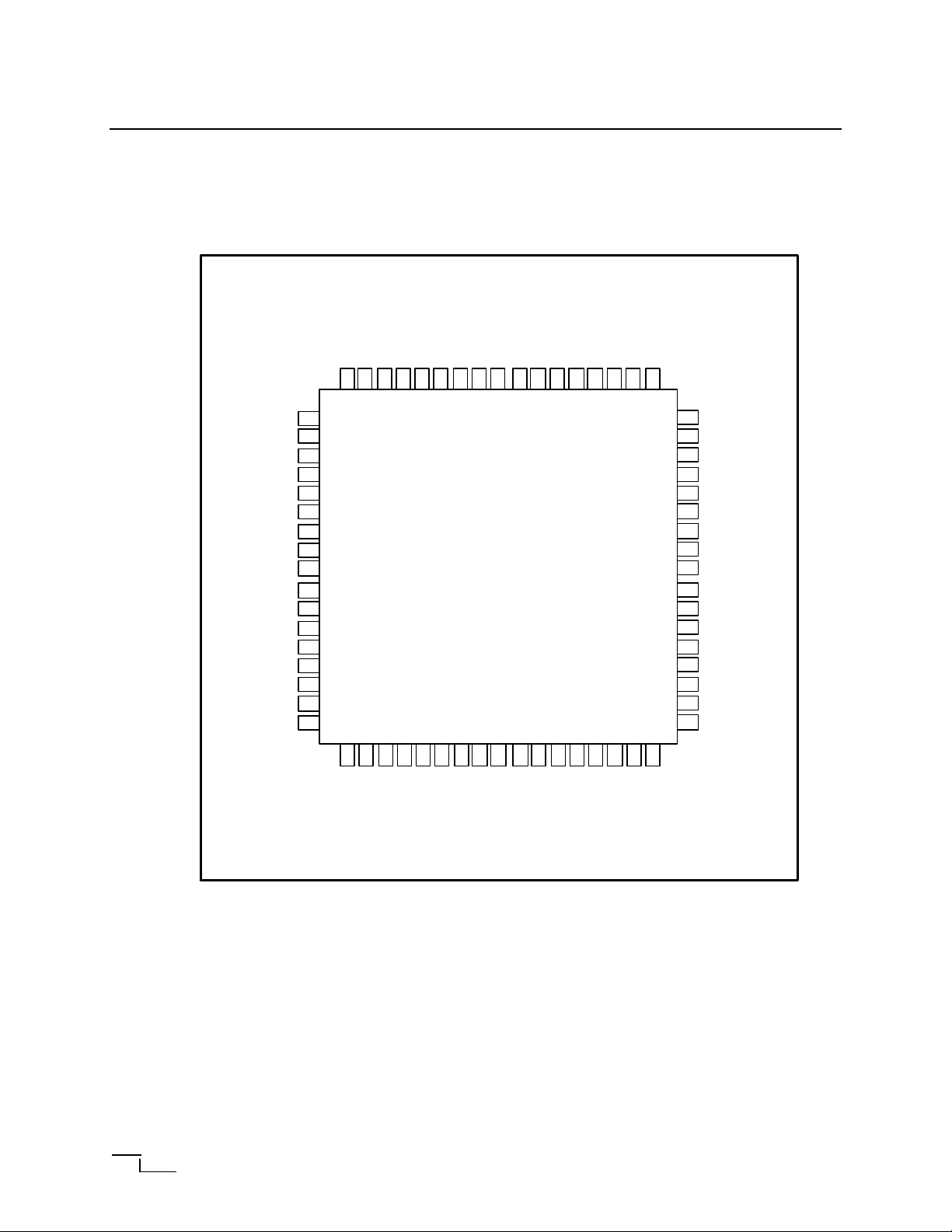
IA63484 Data Sheet
Advanced CRT Controller
68 Pin Package: ACRTC PLCC PINOUT
Pin Arrangement:
dack_n
dtack_n(T)
irq(O,D)
hsync_n
vsync_n
Vcc
exsync_n
Vss
Vss
d0(T)
d1(T)
d2(T)
d3(T)
d4(T)
d5(T)
d6(T)
d7(T)
rs
res_n
dreq_n
done_n(O,D)
27
d9(T)
d8(T)
cs_n
d10(T)
d12(T)
d11(T)
rw_n
O,D: Open Drain
T: Three State
Vcc
cud1_n
cud2_n
19
68
IA63484
Vss
d15(T)
d14(T)
d13(T)
disp1_n
disp2_n
lpstb
ra4
ma_ra18_2
ma_ra19_3
mad3(T)
mad2(T)
mad1(T)
mad0(T)
60
44
mad14(T)
mad15(T)
ma_ra17_1
ma_ra16_0
mad4(T)
chr
mrd
draw_n
as_n
mcyc
Vss
Vss
clk_2
Vcc
mad5(T)
mad6(T)
mad7(T)
mad8(T)
mad9(T)
mad10(T)
mad11(T)
mad12(T)
mad13(T)
Copyright 2001 ENG 21101041200 www.innovasic.com
innovASIC Customer Support:
The End of Obsolescence Page 2 of 32 1−888−824−4184
Page 3
IA63484 Data Sheet
Advanced CRT Controller
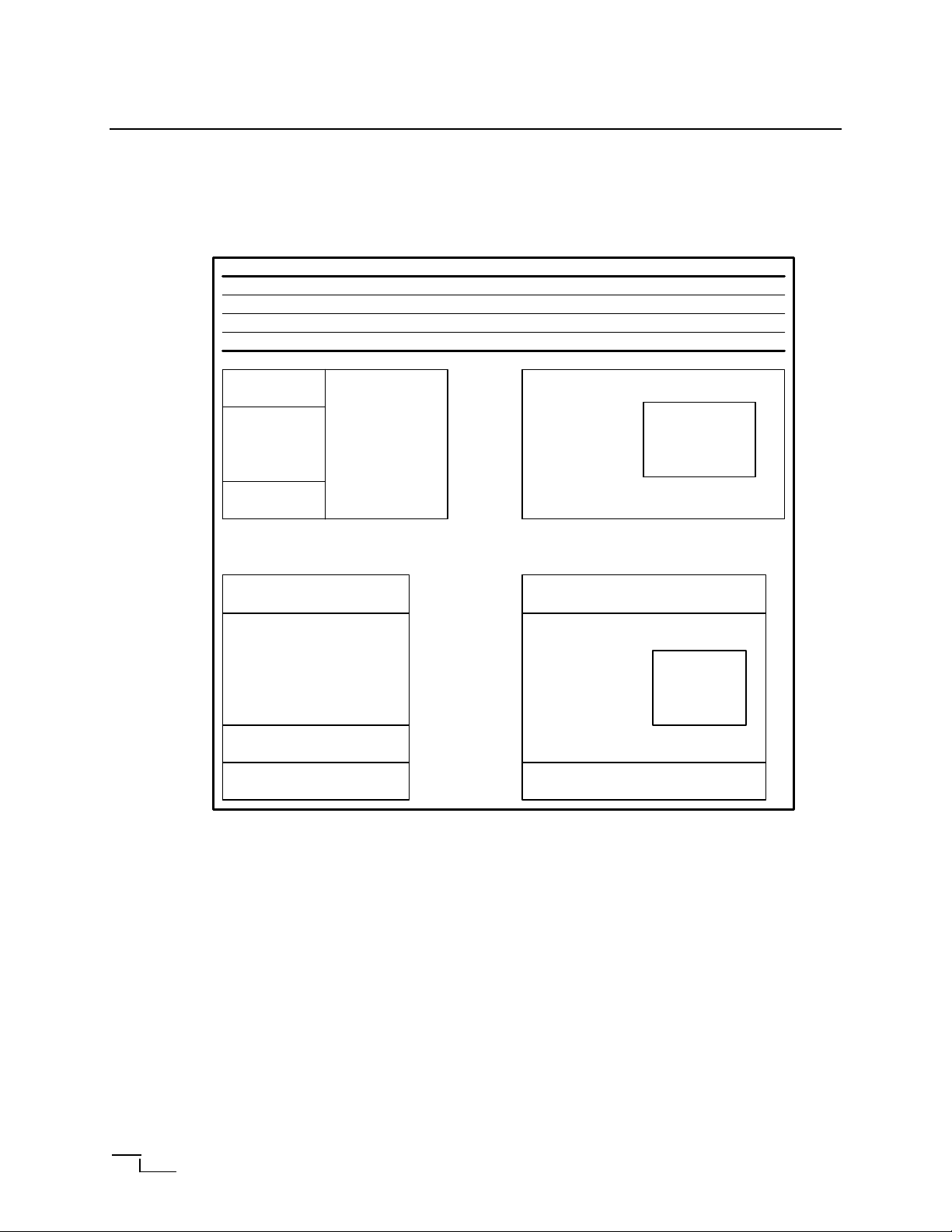
BLOCK DIAGRAM
Figure 1: System Block Diagram
Figure 2 illustrates the ACRTC system environment. The following paragraphs will further describe
the system block diagram and design in more detail.
MPU
(8/16b)
SYSTEM
MEMORY
DMAC
ADDRESS
DATA
res_n
irq_n
d[15:0]
dtack_n
cs_n
rs
rw_n
dreq_n
dack_n
done_n
CONTROL
clk_2
Vss
Vcc
ACRTC
as_n
mrd
disp2_n
disp1_n
cud2_n
cud1_n
lpstb
exsync_n
vsync_n
hsync_n
ma[19:16]
mad[15:0]
FRAME
L
BUFFER
2MB, MAX
DOT SHIFTER
CRT
VIDEO
SIGNAL
Copyright 2001 ENG 21101041200 www.innovasic.com
innovASIC Customer Support:
The End of Obsolescence Page 3 of 32 1−888−824−4184
Page 4
IA63484 Data Sheet
cs_nIChip Select: enables transfers between the host and the ACRTC.
clk_2
I/O
ARTC clock: is the baasic operating clock, twice the frequency of the dot clock.
-*
Higer-order
address
bits/character
screen
rastar
address:MA16/R0-
MA19/RA3
are
Higer-order
character
screen
rastar
address
bit:isthe
high
bitofthe
character
screen
MPU
Advanced CRT Controller
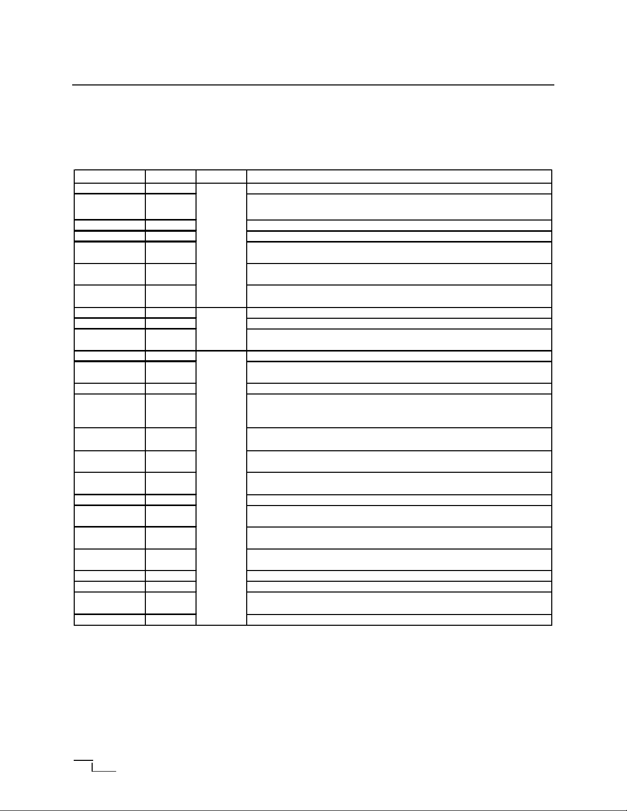
I/O SIGNAL DESCRIPTION:
The diagram below describes the I/O characteristics for each signal on the IC. The signal names
correspond to the signal names on the pinout diagrams provided.
I/O Characteristics:
Signal Name I/O Group Description
res_n I ACRTC reset:
d[15,0]
rw_n I Read/write strobe: controls the direction of host/ACRTC transformers.
I/O
Databus (three state): are the bidirectional data bus to the host mpu or dmac. D0-D
are used in 8-bit data bus mode.
rs
dtack_n
irq_n
dreq_n I DMA request: recieves DMA acknowledge timing from the host DMAC.
dack I/O DMA acknoledge:
done_n
mad[15,0]
as_n O Address strobe: output demultiplexes the address/data bus.
MA16/R0
MA19/RA
RA
chr
mcyc
mrd O Frame buffer memory read: output controls the frame buffer data bus direction.
draw_n
disp1, disp2
cud1, cud2
vsync_n O CRT vertical sync pulse: outputs the crt vertical synchronization pulse.
hsync_n CRT horizontal sync pulse: outputs the crt horizontal synchronization pulse.
exsync_n
lpstb I Lightpen strobe: is the lightpen input
3
4
I
O
O
I
O
O
O
O
O
O
O
I/O
Interface
DMAC
Interface
CRT
Interface
Register Select: selectsthe ACRTC register to be accessed. It isusually connected to
the least significant bit of the host address bus.
Data transfer acknowledge (three state): output provides asynchronous bus cycle
timing. It is compatible with the HD68000 mpu dtack output.
Interrupt request (open drain): output generates interrupt service requests to the
host MPU.
DMA done: terminates DMA transfer. It is compatible with the HD68450 DMAC
DONE signal.
Multiplexed frame buffer address/data bus: are the multiplexed frame buffer
address/data bus.
the upper bits of the graphics screen ddress multiplexed with th lower bits of the
character screen raster address.
raster address (up to 32 rasters.)
Graphic or character screen access: output indicates whether a graphic or character
screen is being accessed.
Frame buffer memory acess timing signal: is the frame buffer access timing output,
1/2 the frequency of clk_2.
Draw/refresh signal: output differentiates between drawing and CRT displayrefresh
cycles.
Display enable: programmable display enable outputs can enable, disable, and blanck
logical screens.
Coursor Display: outputs provides cursor timing programmed by ACRTC parameters
such as cursor definition, cursor mode, cursor address, etc.
External sync:allows synchronization between multiple ACRTSs and other videro
signal generators.
Copyright 2001 ENG 21101041200 www.innovasic.com
innovASIC Customer Support:
The End of Obsolescence Page 4 of 32 1−888−824−4184
Page 5
IA63484 Data Sheet
Advanced CRT Controller
Figure 2: ACRTC Block Diagram
res_n
dreq_n
DMA
dack_n
done_n
irq_n
Control
Unit
Interrupt
Control
Unit
16
d[15:0]
cs_n
rs_n
rw_n
dtack_n
MPU
Interface
ACRTC System Description:
Register
Address
Data
Drawing
Processor
Display
Processor
Timing
Processor
23
25
V
V
cc
SS
20
16
20
15
2
2
draw_adrs[19:0]
draw_data[15:0]
draw_en
write
disp_adrs[19:0]
raster_adrs[4:0]
chr_int
ccud
lpstb
gcud[1:0]
hsync
vsync
exsync
disp[1:0]
m_cyc
as
clk2
CRT
Interface
draw_n
mrd
16
4
2
2
mad[15:0]
ma19_16_ra[3:0]
ra4
chr
lpstb
cud1_n, cud2_n
hsync_n
vsync_n
exsync_n
disp1_n, disp2_n
mcyc
as_n
clk_2
Some CRT controllers provide a single bus interface to the frame buffer that must be shared with the host
MPU. However, refreshing large frame buffers, and accessing the frame buffer for drawing operations can
quickly saturate the shared bus.
The ACRTC uses separate host MPU and frame buffer interfaces. This allows the ACRTC full access to the
frame buffer for display refresh and drawing operations and minimizes the use of the MPU system bus by the
ACRTC. A related benefit is that a large frame buffer (2 MB for each ACRTC) can be used, even if the host
MPU has a smaller address space or segment size restriction.
The ACRTC can use an external Direct Memory Access Controller (DMAC) to increase system throughput
when many commands, parameters and data must be transferred to the ACRTC. Advanced DMAC features
such as the HD68450 “chaining” modes can be used to develop powerful graphics system architectures.
More cost-sensitive or less performance-sensitive applications might not require a DMAC. In these cases, the
interface to the ACRTC can be handled under MPU software control.
While both ACRTC bus interfaces (host MPU and frame buffer) are 16 bits wide, the ACRTC also offers an
8 bit MPU mode for easy connection to popular 8 bit busses.
Copyright 2001 ENG 21101041200 www.innovasic.com
innovASIC Customer Support:
The End of Obsolescence Page 5 of 32 1−888−824−4184
Page 6

IA63484 Data Sheet
Advanced CRT Controller
FUNCTIONAL REQUIREMENTS:
Drawing Processor:
The Drawing Processor performs drawing operations on the frame buffer memory upon interpreting
commands and command parameters issued by the host bus (MPU or DMAC). The drawing
processor then executes ACRTC drawing algorithms and converts lo gical X-Y addresses to physical
frame buffer addresses.
The drawing processor uses three operation control units; the Drawing Algorithm Control unit, the
Drawing Address Generation unit and the Logical Operation unit.
The Drawing Algorithm Control Unit int erprets graphic commands and parameters and executes the
appropriate micro-programmed drawing algorithm. This control unit calculates coordinates using
logical pixel X-Y addressing.
The Drawing Address Generation Unit converts logical X-Y addresses from the Drawing Algorithm
Control unit to a bit address in the frame buffer. The frame buffer is organized as sequential 16 bit
words. The bit address consists of 20 bits and bits 0-4 specifying the logical pixel bit address within
the physical frame buffer word.
Logical Operation Unit, using the address calculated in the drawing algorithm control and drawing
address generation units, performs logical operations between the existing read data in the frame
buffer and the drawing pattern in the pattern RAM, and rewrites the results into the frame buffer. A
detailed description of the Drawing Processor is contained in its module specification.
Display Processor:
The display processor manages frame buffer refresh addressing based on the user specified display
screen organization. It combines and displays as many as 4 independent screen segments (3
horizontal split screens and 1 window) using an internal high-speed address calculation unit. It
controls display refresh outputs in graphic (physical frame buffer address) or character (physical
refresh memory address and row address) modes.
Display Functions:
The ACRTC allows the frame buffer to be divided into four separate logical screens:
• Upper
• Base
• Lower
• Window
In the simplest case, only the base screen parameters must be defined. Other screens may be
selectively enabled, disabled, and blanked under software control.
The background screens (upper, base, and lower) split the screen into three horizontal partitions
whose positions are fully programmable. The window screen is unique, since the ACRTC usually
gives it higher priority than the background screens. A typical application might be to use the base
screen for the bulk of the user interaction, while using the upper screen for pull-down menus and the
lower screen for status line indicators. The exception is in the ACRTC superimpose mode, in which
the window has the same priority as the background screens. In this mode, the window and
Copyright 2001 ENG 21101041200 www.innovasic.com
innovASIC Customer Support:
The End of Obsolescence Page 6 of 32 1−888−824−4184
Page 7
IA63484 Data Sheet
Advanced CRT Controller
background screens are superimposed on the display. Figure 3 is an example of the screen
combinations.
Figure 3: Screen Combination Examples
Screen Number
0
1
2
3
Upper
Base
Lower
Screen Name Screen Group
Upper Screen
Base Screen
Lower Screen
Window Screen
Window
Upper Upper
Base
Background Screen
Base
Base
Window
Window
Lower
Window
Lower
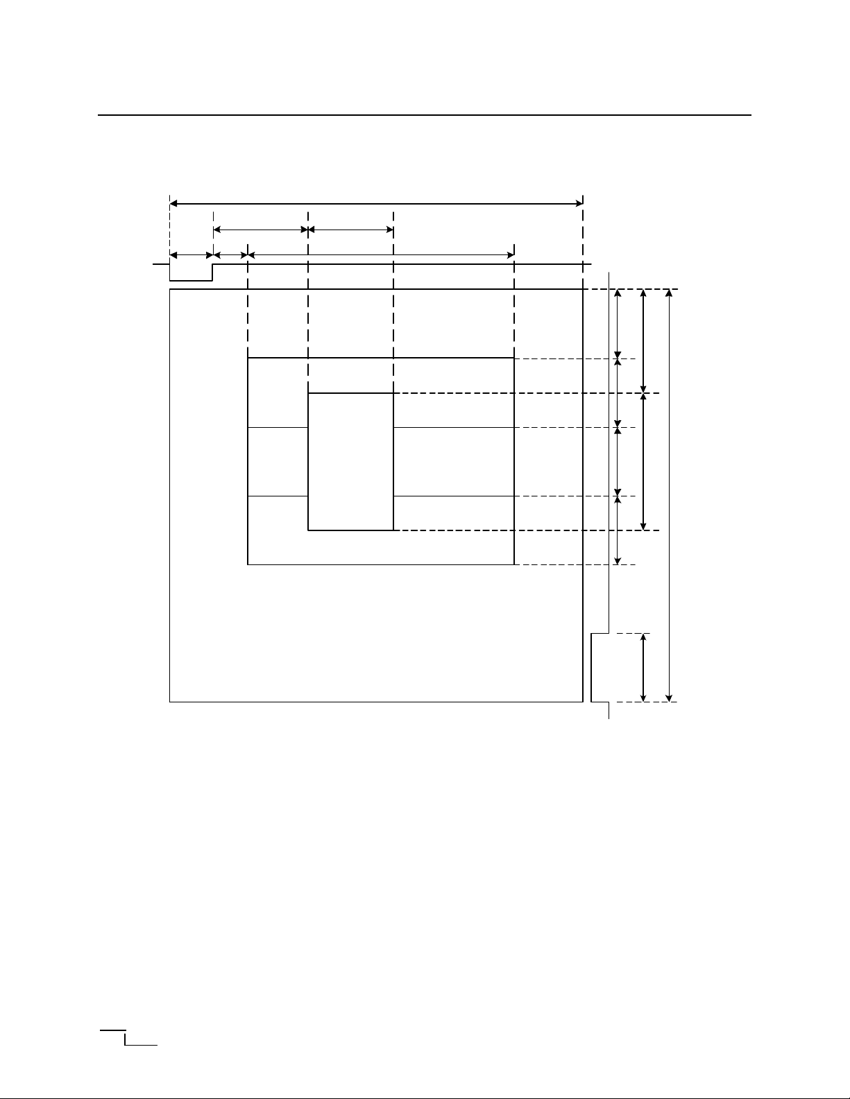
Display Control:
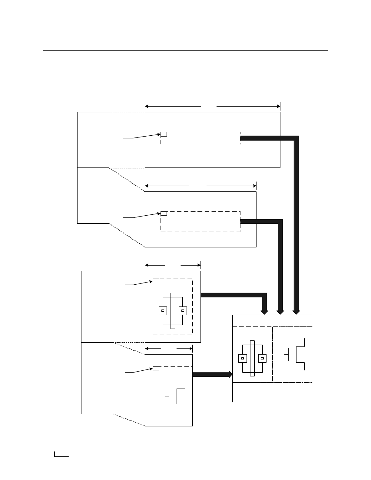
The ACRTC can have two types of external frame memory: 2 Mbyte frame buffer and 128 kbyte
refresh memory. The chr signal controls which memory is accessed.
Each screen has its own memory width, vertical display width, and character/graphic attribution set
by the control registers. Horizontal display control registers are set in units of memory cycles.
Vertical display control registers are set in units of rasters. Figure 4 illustrates the relation between the
frame memory and the display screens, while Figure 5 illustrates the timing.
Note that display width of registers marked with an (*) in Figure 4 is:
Display width = Register value + 1 memory cycle.
Copyright 2001 ENG 21101041200 www.innovasic.com
innovASIC Customer Support:
The End of Obsolescence Page 7 of 32 1−888−824−4184
Page 8
IA63484 Data Sheet
Advanced CRT Controller
Figure 4: Frame Memory and Display Screens
Frame Memory Image
Refresh Memory
(Character)
$0000
MW0
$FFFF
$00000
Frame Buffer
(Graphic)
SA0
SA2
SA1
File Name: MOS
MW2
Left : Layout
Right : Symbol
MW1
File Name: MOS
MW3
SA3
Left : Layout
Right : Symbol
$FFFFF
Copyright 2001 ENG 21101041200 www.innovasic.com
innovASIC Customer Support:
The End of Obsolescence Page 8 of 32 1−888−824−4184
Page 9
IA63484 Data Sheet
Advanced CRT Controller
Figure 5: Display Screen Specification
HC*
hsync_n
HWS* HWW*
HDS*HSW HDW*
Display Screen Period
(Upper)
(Base) (Base)
(Lower)
(Window)
vsync_n
VDS SP0 SP1 SP2
VC
VSWVWS VWW
Timing Processor:
The Timing Processor generates the CRT synchronization signals and signals used internally
by the ACRTC. The details for this block are contained in the module specification for the
Display Processor.
CRT Interface:
The CRT Interface manages the communication between the frame buffer, the light pen and the
CRT. The frame buffer interface manages the frame buffer bus and selects display drawing or
refreshes address outputs. The light pen interface uses a 20-bit address register and a strobe input pin
(lpstb).
Copyright 2001 ENG 21101041200 www.innovasic.com
innovASIC Customer Support:
The End of Obsolescence Page 9 of 32 1−888−824−4184
Page 10
IA63484 Data Sheet
Advanced CRT Controller
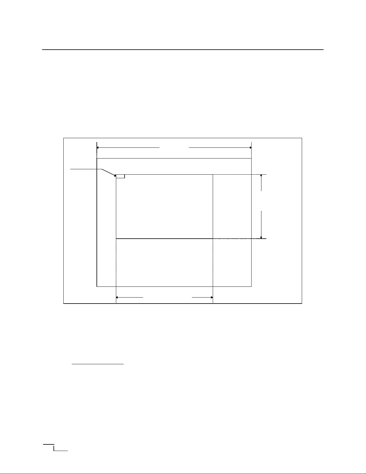
Frame Buffer Interface:
The ACRTC allows for two types of independent frame memories. The first type is up to a 2 Mbyte
frame buffer and the second is a 128 Kbytes refresh memory. The chr output pin can access either
the Graphic or Character screen.
The width of the frame memory is defined by setting-up the memory width register (mwr) and
independently, the horizontal display width is defined by the horizontal display register (hdr). This
allows for the frame buffer area to be bigger than the display area; reference Figure 6.
Figure 6: Frame Memory and Display Screen Area
Memory Width
Start Address
Vertical
Display Screen Area
Display
Width
The ACRTC has two ways to access the frame memory (or buffer); (1) Display Memory Access
(three types) and (2) Graphic Address Increment mode.
Display Memory Access Modes:
In Single Access Mode, a display or drawing cycle is defined as two cycles of clk_2. During the first
cycle, the frame buffer display or drawing address is output. During the second clk_2 cycle, the
frame buffer data is read (display cycles and/or drawing cycles) or written (drawing cycles).
Display and drawing cycles contend for access to the frame buffer. The ACRTC allows the priority
to be defined as display priority or drawing priority. If display has priority, drawing cycles are only
allowed to occur during the horizontal or vertical fly back periods (a ‘flash less’ display is obtained).
If drawing has priority, drawing may occur during display (display may flash).
text
Horizontal Display Width
Copyright 2001 ENG 21101041200 www.innovasic.com
innovASIC Customer Support:
The End of Obsolescence Page 10 of 32 1−888−824−4184
Page 11

IA63484 Data Sheet
Advanced CRT Controller
In Interleaved Access Mode (dual access mode 0), display cycles and drawing cycles are interleaved.
A display or drawing cycle is defined as four cycles of clk_2.
• During the first clk_2 cycle, the ACRTC outputs the frame buffer display address.
• During the second clk_2 cycle, the display data is output from the frame buffer.
• During the third clk_2, the ACRTC outputs the frame buffer drawing address.
• During the fourth clk_2 cycle, the ACRTC reads or writes the drawing data.
In Superimposed Access Mode (dual access mode 1), two separate logical screens are accessed during
each display cycle. The display cycle is defined as four clk_2 cycles. If the third and fourth cycles are
not used for window display, they can be used for drawing; similar to the Interleaved Mode.
• During the first clk_2 cycle, the ACRTC outputs the background screen frame buffer address.
• During the second clk_2 cycle, the background screen displays data.
• During the third clk_2 cycle, the ACRTC outputs the window screen frame buffer address or the
drawing frame buffer address.
• During the fourth clk_2 cycle, the ACRTC reads (display or drawing) or writes (drawing) the
window screen display or drawing data.
Graphic Address Increment (GAI) Mode:
The ACRTC can be programmed to control the graphic display address in one of six ways, by
incrementing by 1, 2, 4, 8, and 16 words, 1 word every two display cycles, and no increment. Setting
GAI to increment by 2, 4, 8, or 16 words per display cycle achieves 2, 4, 8, or 16 times the video data
rate corresponding to GAI = 1. This allows the number of bits/logical pixel and logical pixel
resolution to be increased while meeting the clk_2 maximum frequency constraint.
When the frame buffer memory uses dynamic RAMs (DRAMs), the ACRTC automatically provides
DRAM refresh addressing.
During hsync_n low, the ACRTC outputs the values of an 8-bit DRAM refresh counter on the
multiplexed frame buffer address and data bus mad[15:0]. The counter is decremented on each
frame buffer access. The refresh address pin assignment (mad[15:0]) depends on the GAI mode.
The remaining mad and ma19_16_ra outputs not used for refresh addressing are cleared to a low
value.
Table 1: GAI and DRAM Refresh Addressing
Address Increment Mode Refresh Address Output Terminal
+1 (GAI = 000) mad[7:0]
+2 (GAI = 001) mad[8:1]
+4 (GAI = 010) mad[9:2]
+8 (GAI = 011) mad[10:3]
+16 (GAI = 100) mad[11:4]
+0 (GAI = 101) mad[7:0]
+1/2 (GAI = 11X) mad[7:0]
Copyright 2001 ENG 21101041200 www.innovasic.com
innovASIC Customer Support:
The End of Obsolescence Page 11 of 32 1−888−824−4184
Page 12

IA63484 Data Sheet
Advanced CRT Controller
Address Space:
The ACRTC allows the host to issue commands in logical X-Y coordinates. The ACRTC then
converts the physical linear word addresses with bit field offsets in the frame buffer. Figure 7 shows
the relationship between the logical X-Y screen address and the frame buffer memory. The frame
buffer memory is organized as sequential 16 bit words. The host may specify 1, 2, 4, 8, or 16 physical
bits in the frame buffer. The system in the figure uses 4 bit logical pixels, allowing for 16 colors or
tones.
Figure 7: Logical/Physical Addressing
Physical Addressing
(Frame Buffer)
1 pixel data
bit
15
bit
0
SAD
Logical Addressing
Origin
Display Screen
Y
(x,y)
X
MW
Y
(x,y)
X
SAD
Origin
MW
Up to 4 logical screens may be mapped onto the ACRTC physical address space. The four screens
are the upper, base, lower, and window screens. The host first specifies the following:
• A logical screen starting address.
• A logical screen physical memory width (memory words per raster).
• A logical pixel physical memory width (bit per pixel).
• A logical origin physical address.
Then the ACRTC converts the logical pixel X-Y addresses issued by the host MPU or the drawing
processor to physical frame buffer addresses. The device also performs bit extraction and masking
to map logical pixel operations to 16 bit word frame buffer addresses.
Copyright 2001 ENG 21101041200 www.innovasic.com
innovASIC Customer Support:
The End of Obsolescence Page 12 of 32 1−888−824−4184
Page 13

IA63484 Data Sheet
Advanced CRT Controller
Memory Map:
The ACTRC has over 200 bytes of accessible registers organized as Hardware, Direct, and FIFO
Access. Figure 8 illustrates the programming memory map model.
• The ACRTC registers are initialized by res_n as follows:
• Drawing and display operations are stopped
• Status register (SR) is initialized to $FF23
• Command control register (CCR) is initialized to $8000.
• Operation mode register bits MS and STR are reset to 0.
• All other registers are unaffected by res_n.
• The FIFO Entry (FE) pointer is cleared, and the written command/parameter and the read
data are lo st.
• The DRAM refresh address is placed on the mad lines determined by graphic address
increment (GAI). Refresh continues to function until the start bit (STR) is set to 1. hsync_n
is also held low during the period from res_n until str is set by the MPU.
For directly accessible registers, the register address is shown as ‘rXX’, and FIFO accessible registers
are shown as ‘PrXX’, where XX is interpreted as an 8 bit hexadecimal value. Hexadecimal numbers
are denoted by a leading ‘$’.
Copyright 2001 ENG 21101041200 www.innovasic.com
innovASIC Customer Support:
The End of Obsolescence Page 13 of 32 1−888−824−4184
Page 14

IA63484 Data Sheet
Advanced CRT Controller
Figure 8: Programming Model
Address Register
Status Register
FIFO Entry
Command Control Register
Operation Mode Register
Display Control Register
Write FIFO
Raster Counter
Horizontal Sync
Horizontal Display
Vertical Sync
Vertical Display
Split Screen Width
Blink Control
Horizontal Window Display
Vertical Window Display
Graphic Cursor
Split Screen 0
(Upper Screen)
Split Screen 1
(Base Screen)
Split Screen 2
(Lower Screen)
Split Screen 3
(Window Screen)
Pattern
RAM
Read FIFO
Command Register
16 x 16
Color 0
Color Comparison
Edge Color
Mask
Pattern RAM Control
Block Cursor
Cursor Definition
Zoon Factor
Light Pen Address
Drawing
Parameter
Register
Area Definition
Read/Write Pointer
Drawing Pointer
Current Pointer
Copyright 2001 ENG 21101041200 www.innovasic.com
innovASIC Customer Support:
The End of Obsolescence Page 14 of 32 1−888−824−4184
Page 15

IA63484 Data Sheet
Advanced CRT Controller
Hardware Access:
The ACRTC is connected to the host MPU as a standard memory-mapped peripheral that occupies
two word locations of the host’s address space. When rs=0, read operations access the status
register, and write operations access the address register.
The status register summarizes the ACRTC State; it monitors the overall state of the ACRTC for the
host MPU. When the MPU wants to access a direct access register, it puts the register’s address into
the ACRTC address register.
Direct Access:
The MPU accesses the direct access registers by loading the register address into the address register.
Then, when the MPU accesses the ACRTC with rs=1, the chosen register is accessed. The FIFO
entry register enables the MPU to access FIFO access registers using the ACRTC read and write
FIFOs.
The command control register controls overall ACRTC operations, such as aborting or pausing
commands, defining DMA protocols, and enabling/disabling interrupt sources.
The operation mode register defines basic parameters of ACRTC operation, such as frame buffer
access mode, display or drawing priority, cursor and display timing skew factors, and raster scan
mode.
The display control register independently enables and disables the four ACRTC logical address
screens (upper, base, lower, and window). It also contains 8 user-defined video attribute bits.
The timing control RAM registers define ACRTC timing, including timing specifications for CRT
control signals (hsync_n, vsync_n, etc.), logical display screen size and display period, and blink
period.
The display control RAM contains registers that define logical screen display parameters, such as start
address, raster address, and memory width. It also includes the cursor definition, zoom factor, and
lightpen registers.
FIFO Access:
For high-performance drawing, key drawing processor registers are coupled to the host MPU via the
ACRTC’s 16-byte read and write FIFOs. Figure and Figure illustrate the hardware and direct access
register information.
ACRTC commands are sent from the MPU via the write FIFO to the command register. As the
ACRTC completes a command, the next command is automatically fetched from the write FIFO and
put into the command register.
The pattern RAM defines drawing and painting patterns. It is accessed with the ACRTC’s Read
Pattern RAM (RPTN) and Write Pattern RAM (WPTN) register access commands.
The drawing parameter registers define detailed parameters of the drawing process, such as color
data, area control (hitting/clipping), and pattern RAM pointers. The drawing parameter registers are
accessed using the ACRTC’s Read Parameter Register (RPR) and Write Parameter Register (WPR)
commands. Figure illustrates the drawing parameter registers.
Copyright 2001 ENG 21101041200 www.innovasic.com
innovASIC Customer Support:
The End of Obsolescence Page 15 of 32 1−888−824−4184
Page 16

IA63484 Data Sheet
Advanced CRT Controller
Figure 9: Hardware Access and Direct Access Registers
Reg Name Reg # 15 14 13 12 11 10 9 8 7 6 5 4 3 2 1 0
Address
Reg(AR)
Status
Reg(SR)
FIFO
Entry(FE)
Command
Control
(CCR)
Operation
Mode (OMR)
Display
Control
(DCR)
Undefined
Raster
Count(RCR)
Horizontal
Sync(HSR)
Horizontal
Display
(HDR)
AR $0 Address
ST $0
$00 FIFO Entry
$02
$04
$06
$08-$7E, $9E-
$BE, $F0-$FE
$80 $0 RC
$82 HC $0 HSW
$84 HDS HDW 0, 1, 0/1
ABT PSE DDM CDM DRC
MS STR ACP WSS
DSP SE1 SE0 SE2 SE3 ATR 0, 1, 0/1
GBM
CSK DSK
CER ARD CED LPD RFF RFR WFR WFE
CRE ARE CEE LPE RFE RRE WRE WEE
RAM
$0
GAI ACM RSM 0, 1, 0/1
cs_n, rs,
rw_n
0, 0, 0
0, 0, 0
0, 1, 0/1
0, 1, 0/1
0, 1, 0/1
0, 1, 1
0, 1, 0/1
Vertical
Sync(VSR)
Vertical
Display
(VDR)
Split Screen
Width(SSW)
Blink Control
(BCR)
Horz.
Window
Disp(HWR)
Vert. Window
Disp(VDR)
Graphic
Cursor
(GCR)
$86 $0 VC 0, 1, 0/1
VSW$88 VDS $0 0, 1, 0/1
$8A $0 SP1
$8C $0 SP0
$8E $0 SP2
$90 BON1 BOFF1 BON2 BOFF2
$92 HWS HWW
$94 $0 VWS
$96 $0 VWW
$98 CXE CXS
$9A $0 CSY
$9C $0 CYE
0, 1, 0/1
0, 1, 0/1
0, 1, 0/1
0, 1, 0/1
0, 1, 0/1
0, 1, 0/1
0, 1, 0/1
0, 1, 0/1
0, 1, 0/1
0, 1, 0/1
Copyright 2001 ENG 21101041200 www.innovasic.com
innovASIC Customer Support:
The End of Obsolescence Page 16 of 32 1−888−824−4184
Page 17

IA63484 Data Sheet
Advanced CRT Controller
Figure 10: Hardware Access and Direct Access Registers (cont.)
Reg Name Reg # 14 13 12 11 10 9 8 7 6 5 4 3 2 1 0 cs_n, rs, rw_n
Raster
Addr 0
(RAR0)
Memry
Wdth 0
(MWR0)
Strt Addr 0
(SAR0)
Raster
Addr 1
(RAR1)
Mem
Width 1
(MWR1)
Strt Addr 1
(SAR1)
Raster
Addr 2
(RAR2)
Memry
Wdth 2
(MWR2)
Strt Addr 2
(SAR2)
Raster
Addr 3
(RAR3)
Memry
Wdth 3
(MWR3)
Strt Addr 3
(SAR3)
Blk Cursor
1 (BCUR1)
$C0(Upper
Scrn)
$C2(Upper
Scrn)
$C4(Upper
Scrn)
$C6(Upper
Scrn)
$C8(Base
Scrn)
$CA(Base
Scrn)
$CC(Base
Scrn)
$CE(Base
Scrn)
$D0(Lower
Scrn)
$D2(Lower
Scrn)
$D4(Lower
Scrn)
$D6(Lower
Reg #
Scrn)
$D8(Wndw
Scrn)
$DA(Wndw
Scrn)
$DC(Wndw
Scrn)
$DE(Wndw
Reg #
Scrn)
$E0 BCW1 $0BCSR1 BCER1
$E2 BCA1
15
$0 $0LRA0 FRA0 0, 0, 0
CH
R
CH
R
CH
R
CH
R
$0 MW0 0, 0, 0
$0 SDA0 $0 SA0H/SRA0 0, 1, 0/1
SA0L
$0 LRA1 $0 FRA1 0, 1, 0/1
MW1$0 0, 1, 0/1
$0 SA1H/SRA1SDA1 $0 0, 1, 0/1
SA1L
$0 $0LRA2 FRA2 0, 1, 0/1
MW2$0 0, 1, 0/1
$0 SA2H/SRA2SDA2 $0 0, 1, 0/1
SA2L
$0 $0LRA3 FRA3 0, 1, 0/1
MW3$0 0, 1, 0/1
$0 SA3H/SRA3SDA3 $0
SA3L
0, 1, 0/1
0, 1, 1
cs_n, rs, rw_n0, 1, 0/1
0, 1, 0/1
cs_n, rs, rw_n0, 1, 0/1
0, 1, 0/1
0, 1, 0/1
Blk Cursor
2 (BCUR2)
Cursor Def.
(CDR)
Zoom
Factor
(ZFR)
Lightpen
Addr
(LPAR)
$E4 BCW2 $0BCSR2 BCER2
$E5 BCA2
$E8 CM CON1 COFF1 $0 CON2 COFF2 0, 1, 0/1
$EA HZF VZF $0 0, 1, 0/1
$EC $0 FRA3
$EE LPAL
CH
R
$0 0, 1, 0/1
0, 1, 0/1
0, 1, 0/1
0, 1, 0/1
Copyright 2001 ENG 21101041200 www.innovasic.com
innovASIC Customer Support:
The End of Obsolescence Page 17 of 32 1−888−824−4184
Page 18

IA63484 Data Sheet
Advanced CRT Controller
Figure 11: Drawing Parameter Registers
Reg Name Reg # 15 14 13 12 11 10 9 8 7 6 5 4 3 2 1 0 Read/Write
Color 0 (CL0) Pr00 CL0 R/W
Color 1 (CL1) Pr01 CL1 R/W
Color Cmpr
(CCMP)
Edge Color
(EDG)
Mask
(MASK)
Pattern RAM
Control
(PRC)
Area
Def(ADR)->
Set 2's Comp.
for neg.
values of X
and Y axis.
Read Write
Pntr (RWP)
Undefined
Drawing Pntr
(DP)
Pr02 CCMP R/W
Pr03 EDG R/W
Pr04 MASK R/W
Pr05 R/W
Pr06 R/W
Pr07 R/W
Pr08 XMIN R/W
Pr09 YMIN R/W
Pr0A XMAX R/W
Reg #
Pr0C YMAX R/W
Pr0C R/W
Pr0D RWPL R/W
Pr0E-Pr0F,
Pr14-Pr15
Pr10 R
Pr11 R
PPY PZCY PPX PZCX
PSY $0 PSX $0
PEY PZY PEX PZX
15
DN $0 RWPH
$0
$0 R/W
DN $0 DPAH
DPAL DPD
cs_n, rs, rw_n
Current
Pntr(CP)->
Set 2's Comp.
for neg.
values
Pr12 R
Pr13 R
X
Y
Copyright 2001 ENG 21101041200 www.innovasic.com
innovASIC Customer Support:
The End of Obsolescence Page 18 of 32 1−888−824−4184
Page 19

IA63484 Data Sheet
Advanced CRT Controller
COMMAND TRANSFER MODES:
Program Transfer and DMA Transfer are the two modes used to transfer commands and associated
parameters issued by the MPU to the ACRTC.
Program Transfer:
Program transfer occurs when the MPU specifies the FIFO entry address and then writes operation
code/parameters to the write FIFO under program control. The MPU writes are normally
synchronized with ACRTC FIFO status by software polling or interrupts.
Software Polling (WFR, WFE interrupts disabled):
• MPU program checks the SR for WFR=1, and then writes 1-word operation code/parameters, or
• MPU program checks the SR for write WFE=1, and the writes 1- to 8-word operation
code/parameters.
Interrupt Driven (WFR, WFE interrupts enabled):
• MPU WFR interrupt service routine writes 1-word operation code/parameters, or
• MPU WFE interrupt service routine writes 1- to 8-word operation code/parameters.
DMA Transfer:
Commands and parameters can be transferred from MPU system memory by an external DMAC.
The MPU initiates and terminates command DMA transfer mode under software control.
Command DMA can also be terminated by assertion of the done_n input.
Using command DMA transfer, the ACRTC will issue cycle stealing DMA requests to the DMAC
when the write FIFO is empty. The DMA data is automatically sent from system memory to the
ACRTC write FIFO regardless of the contents of the address register.
Command Function:
The ACRTC commands are divided into three groups, register access commands, data transfer
commands, and graphic drawing commands.
Register access commands:
Access to the drawing processor drawing parameter registers and the pattern RAM is through the
read/write FIFOs using register access commands. When writing register access commands to an
initially empty write FIFO, the MPU does not have to synchronize to write FIFO status. The
ACRTC can fetch and execute these commands faster than the MPU can issue them.
Data transfer commands:
Data is moved between the host system memory and the frame buffer, or within the frame buffer
using the data transfer commands. Before issuing these commands, a physical 20-bit frame buffer
address must be specified in the RWP (read/write pointer) drawing parameter register.
Copyright 2001 ENG 21101041200 www.innovasic.com
innovASIC Customer Support:
The End of Obsolescence Page 19 of 32 1−888−824−4184
Page 20

IA63484 Data Sheet
∑
∑
∑
∑
Advanced CRT Controller
Graphic Drawing Commands:
The graphic drawing commands cause the ACRTC to draw. Graphic drawing is performed by
modifying the contents of the frame buffer based on micro coded drawing algorithms in the ACRTC
drawing processor. Parameters for these commands are specified using logical X-Y addressing. The
display processor performs the complex task of translating a logical pixel address to a linear frame
buffer word address, and further, selecting the proper sub field of the word.
Many instructions allow specification in either absolute or relative X-Y co ordinates. In both cases,
two’s compliment numbers represent both positive and negative values.
Table 2 and Table 3 tabulate the ACRTC drawing commands and Op-Codes available.
Table 2: ACRTC Command Table
Type Mnemonic Command Name # (words) CLK_2 Cycles
ORG Origin 3 8
WPR Write Parameter Reg 2 6
Register Access Command
Data Transfer Command
Graphic Drawing Command
RPR Read Parameter Reg 1 6
WPTN Write Pattern RAM n+2 4n+8
RPTN Read Pattern RAM 2 4n+10
DRD DMA Read 3 (4x+8)y+12(x*y/8 )+(62~68)
DWT DMA Write 3 (4x+8)y+16(x*y/8 )+34
DMOD DMA Modify 3 (4x+8)y+16(x*y/8 )+34
RD Read 1 12
WT Write 2 8
MOD Modify 2 8
CLR Clear 4 (2x+8)y+12
SCLR Selective Clear 4 (4x+8)y+12
CPY Copy 5 (6x+8)y+12
SCPY Selective Copy 5 (6x+8)y+12
AMOVE Absolute Move 3 56
RMOVE Relative Move 3 56
ALINE Absolute Line 3 P*L+18
RLINE Relative Line 3 P*L+18
ARCT Absolute Rectangle 3 2P(A+B)+54
RRCT Relative Rectangle 3 2P(A+B)+54
APLL Absolute Polyline 2n+2
RPLL Relative Polyline 2n+2
APLG Absolute Polygon 2n+2
RPLG Relative Polygon 2n+2
CRCL Circle 2 8d+66
ELPS Ellipse 4 10d+90
AARC Absolute Arc 5 8d+18
RARC Relative Arc 5 8d+18
AEARC Absolute Ellipse Arc 7 10d+96
REARC Relative Ellipse Arc 7 10d+96
AFRCT Absolute Filled Rectangle 3 (P*A+8)B+18
RFRCT Relative Filled Rectangle 3 (P*A+8)B+18
PAINT Paint 1 (18A+102)B-58(Applies to rectagular figures, varies for other shapes)
DOT Dot 1 8
PTN Pattern 2 (P*A+10)B+20
AGCPY Absolute Graphic Copy 5 ((P+2)A+10)B+70
RGCPY Relative Graphic Copy 5 ((P+2)A+10)B+70
↑
↑
↑
++ 8)16*( LP
++ 8)16*( LP
+++ 20*)16*( LoPLP
+++ 20*)16*( LoPLP
Copyright 2001 ENG 21101041200 www.innovasic.com
innovASIC Customer Support:
The End of Obsolescence Page 20 of 32 1−888−824−4184
Page 21

IA63484 Data Sheet
Advanced CRT Controller
Table 3: Opcode Map
Type
Register Access Command
Data Transfer Command
Graphic Drawing Command
Mnemonic Operation Code Parameter
ORG 0 0 0 0 0 1 0 0 0 0 0 0 0 0 0 0 DPH DPL
WPR 0 0 0 0 1 0 0 0 0 0 0 RN D
RPR 0 0 0 0 1 1 0 0 0 0 0 RN
WPTN 0 0 0 1 1 0 0 0 0 0 0 0 PRA n D1,...,Dn
RPTN 0 0 0 1 1 1 0 0 0 0 0 0 PRA n
DRD 0 0 1 0 0 1 0 0 0 0 0 0 0 0 0 0 AX AY
DWT 0 0 1 0 1 0 0 0 0 0 0 0 0 0 0 0 AX AY
DMOD 0 0 1 0 1 1 0 0 0 0 0 0 0 0 MM AX AY
RD 0 1 0 0 0 1 0 0 0 0 0 0 0 0 0 0
WT 0 1 0 0 1 0 0 0 0 0 0 0 0 0 0 0 D
MOD 0 1 0 0 1 1 0 0 0 0 0 0 0 0 MM D
CLR 0 1 0 1 1 0 0 0 0 0 0 0 0 0 0 0 D AX AY
SCLR 0 1 0 1 1 1 0 0 0 0 0 0 0 0 MM D AX AY
CPY 00 1 1 0 S DSD 0 0 0 0 0 0 0 0 SAH SAL AX AY
SCPY 01 1 1 1 S DSD 0 0 0 0 0 0 MM SAH SAL AX AY
AMOVE 1 0 0 0 0 0 0 0 0 0 0 0 0 0 0 0 X Y
RMOVE 1 0 0 0 0 1 0 0 0 0 0 0 0 0 0 0 dX dY
ALINE 1 0 0 0 1 0 0 0 AREA COL OPM X Y
RLINE 1 0 0 0 1 1 0 0 AREA COL OPM dX dY
ARCT 1 0 0 1 0 0 0 0 AREA COL OPM X Y
RRCT 1 0 0 1 0 1 0 0 AREA COL OPM dX dY
APLL 1 0 0 1 1 0 0 0 AREA COL OPM n X1,Y1,...XN,YN
RPLL 1 0 0 1 1 1 0 0 AREA COL OPM n dX1,dY1,...dXN,dYN
APLG 1 0 1 0 0 0 0 0 AREA COL OPM n X1,Y1,...XN,YN
RPLG 1 0 1 0 0 1 0 0 AREA COL OPM n dX1,dY1,...dXN,dYN
CRCL 1 0 1 0 1 0 0 C AREA COL OPM r
ELPS 1 0 1 0 1 1 0 C AREA COL OPM a b DX
AARC 1 0 1 1 0 0 0 C AREA COL OPM Xc Yc Xe Ye
RARC 1 0 1 1 0 1 0 C AREA COL OPM dXc dYc dXe dYe
AEARC 1 0 1 1 1 0 0 C AREA COL OPM a b Xc Yc Xe Ye
REARC 1 0 1 1 1 1 0 C AREA COL OPM a b dXc dYc dXe dYe
AFRCT 1 1 0 0 0 0 0 0 AREA COL OPM X Y
RFRCT 1 1 0 0 0 1 0 0 AREA COL OPM dX dY
PAINT 1 1 0 0 1 0 0 E AREA 0 0 000
DOT 1 1 0 0 1 1 0 0 AREA COL OPM
PTN 1 1 0 1 SL SD AREA COL OPM SZ
AGCPY 1 1 1 0 S DSD AREA 0 0 OPM Xs Ys DX DY
RGCPY 1 1 1 1 S DSD AREA 0 0 OPM dXs dYs dDX dDY
Copyright 2001 ENG 21101041200 www.innovasic.com
innovASIC Customer Support:
The End of Obsolescence Page 21 of 32 1−888−824−4184
Page 22

IA63484 Data Sheet
Advanced CRT Controller
AC/DC PARAMETERS:
Absolute maximum ratings:
Operating Temp (Comm’l)…….......................………………...…..0°C to +70°C
Storage Temperature.......................................…....……....……...…- 65°C to 150°C
VCC Supply Voltage…………......................................………..…... - 0.3V to +4.6V
Input Voltage Range…...............................................…..................... - 0.3V to +4.6V
Allowable Input Current……………………………………….…………. TBD
Total Allowable Input Current……………………………………………..TBD
Recommended Operating Conditions (@ 9.8 MHz):
Power Supply VCC………………………………………………..4.75V to 5.25V
Input Low Voltage VIL……………………………………………..…0V to 0.8V
Input High Voltage VIH…………………………………………...….2.0V to V
Operating Temperature Range…………………………………….....0°C to 70°C
DC Characteristics:
Item Symbol Min Max Unit Test Conditions
Input High Level
Voltage
Input Low Level
Voltage
Input Leak
Current
Hi-Z Input
Current
Output High
Level Voltage
Output Low
Level Voltage
Output Leak
Current(Hi-Z)
All Inputs VIH 2.0 - V 9.8 MHz
All Inputs VIL - 0.8 V 9.8 MHz
rw_n, cs_n, rs, res_n,
Iin -10 10 uA V
dack_n, clk_2, lpstb
d[15:0], mad[15:0],
I
-10 10 uA V
TSI
exsync_n
d[15:0], mad[15:0],
VOH 0.7Vcc uA IOH = -4mA
exsync_n, cud1_n,
cud2_n, dreq_n,
dtack_n, hsync_n,
vsync_n, mrd,
draw_n, as_n,
disp1_n, disp2_n, chr,
mcyc, ra4, ma16/ra 0,
ma19/ra3
d[15:0], mad[15:0],
exsync_n, cud1_n,
cud2_n, dreq_n,
dtack_n, hsync_n,
vsync_n, mrd,
draw_n, as_n,
disp1_n, disp2_n, chr,
mcyc, ra4, ma16/ra0,
ma19/ra3
irq_n, done_n
irq_n, done_n I
V
OL
VOL
TBD uA V
LOD
0.3VCC
0.3VCC
CC
V
V
SS to VCC
SS to VCC
CMOS Output
I
= 4mA
OL
CMOS Output
I
= 4mA Open
OL
Drain
= VCC
OH
Copyright 2001 ENG 21101041200 www.innovasic.com
innovASIC Customer Support:
The End of Obsolescence Page 22 of 32 1−888−824−4184
Page 23

IA63484 Data Sheet
Advanced CRT Controller
Item Symbol Min Max Unit Test Conditions
Input Capacitance d[15:0], mad[15:0],
exsync_n, rw_n, cs_n,
rs, res_n, dack_n,
clk_2, lpstb
Output
Capacitance
CurrentConsumption
(VCC = 5.0V+5%, VSS = 0V, Ta = 0 to 70oC, unless otherwise noted.)
irq_n, done_n C
ICC TBD mA 9.8 MHz
CIN TBD pF TBD
TBD pF TBD
OUT
Copyright 2001 ENG 21101041200 www.innovasic.com
innovASIC Customer Support:
The End of Obsolescence Page 23 of 32 1−888−824−4184
Page 24

IA63484 Data Sheet
Advanced CRT Controller
AC Characteristics:
Clock Timing:
Item Symbol
Unit
Min Max
Operation Frequency of clk_2 f 1 9.8 MHz
9.8 MHz Version
Clock Cycle Time t
Clock High Level Pulse Width
Clock Low Level Pulse Width t
Clock Rise Time
Clock Fall Time
t
PWCH
PWCL
CYC
t
cr
t
cf
102 1000 ns
46 500 ns
46 500 ns
5 ns
5 ns
MPU Read / Write Cycle Timing:
Item Symbol
rw_n Setup Time
rw_n Hold Time t
rs Setup Time
rs Hold Time t
cs_n Setup Time
cs_n High Level Width
t
RWS
RWH
t
RSS
RSH
t
CSS
t
WCSH
9.8 MHz Version
Min Max
50 ns
0 ns
50 ns
0 ns
40 ns
60 ns
Unit
Read Wait Time
Read Data Access Time t
Read Data Hold Time
Read Data Turn Off Time t
dtack_n Delay Time (Z to L)
dtack_n Delay Time (D to L) t
dtack_n Release Time (L to H)
dtack_n Turn Off Time (H to Z) t
Data Bus 3-State Recovery Time 1
Write Wait Time
Write Data Setup Time t
Write Data Hold Time
t
RWAI
RDAC
t
RDH
RDZ
t
DTKZL
DTKDL
t
DTKLH
DTKZ
t
DBRT1
t
WWAI
WDS
t
WDH
0 ns
80 ns
10 ns
60 ns
70 ns
0 ns
80 ns
100 ns
0 ns
0 ns
40 ns
10 ns
Copyright 2001 ENG 21101041200 www.innovasic.com
innovASIC Customer Support:
The End of Obsolescence Page 24 of 32 1−888−824−4184
Page 25

IA63484 Data Sheet
Advanced CRT Controller
AC Characteristics (continued):
DMA Read / Write Cycle Timing:
Item Symbol
dreq_n Delay Time 1 t
dreq_n Delay Time 2 t
DMA r / w_n Setup Time t
DMA r / w_n Hold Time t
dack_n Setup Time t
dack_n Hold Time t
DMA Read Wait Time
DMA Read Data Access Time
DMA Read Data Hold Time
DMA Read Data Turn Off Time
DMA dtack_n Delay Time (Z to L)
DMA dtack_n Delay Time (D to L)
DMA dtack_n Release Time (L to H)
DMA dtack_n Turn Off Time (H to Z)
done_n Output Delay Time
done_n Output Turn Off Time
Data Bus 3-State Recovery Time 2
done_n Input Pulse Width
DMA Write Wait Time
DMA Write Data Setup Time
DMA Write Data Hold Time t
DRQD1
DRQD2
DMRWS
DMRWH
DAKS
WDAKH
t
DRW
t
DRDAC
t
DRDH
t
DRDZ
t
DDTZL
t
DDTDL
t
DDTLH
t
DDTHZ
t
DND
t
DNL2
t
DBRT2
t
DNPW
t
DWW
t
DWDS
DWDH
9.8 MHz Version
Min Max
110 ns
70 ns
50 ns
0 ns
40 ns
60 ns
0 ns
80 ns
10 ns
60 ns
70 ns
0 ns
80 ns
100 ns
70 ns
80 ns
0 ns
2
0 ns
40 ns
10 ns
Unit
t
CYC
Copyright 2001 ENG 21101041200 www.innovasic.com
innovASIC Customer Support:
The End of Obsolescence Page 25 of 32 1−888−824−4184
Page 26

IA63484 Data Sheet
Advanced CRT Controller
AC Characteristics (continued):
Frame Memory Read / Write Cycle Timing:
Item
as_n "Low" Level Pulse Width
Memory Address Hold Time 2
as_n Delay Time 1
as_n Delay Time 2
Memory Address Delay Time
Memory Address Hold Time 1
Memory Address Turn Off Time (A to Z)
Memory Read Data Setup Time
Memory Read Data Hold Time
ma_ra Delay Time
ma_ra Delay Time
MCYC Delay Time
mrd Delay Time t
mrd Hold Time t
draw_n Delay Time t
draw_n Hold Time t
Memory Write Data Delay Time t
Memory Write Data Hold Time t
Memory Address Setup Time 1 t
Memory Address Setup Time 2 t
NOTE: t
is independent of clk_2 operation frequency (f) and timing of t
MAD
Symbol
t
PWASL
t
MAH2
t
ASD1
t
ASD2
t
MAD
t
MAH1
t
MAAZ
t
MRDS
t
MRDH
t
MARAD
t
MARAH
t
MCYCD
MRDD
MRH
DRWD
DRWH
MWDD
MWDH
MAS1
MAS2
9.8 MHz Version
Min Max
20 ns
5 ns
50 ns
5 40 ns
10 50 ns
15 ns
35 ns
30 ns
0 ns
60 ns
5 ns
5 40 ns
50 ns
5 ns
50 ns
5 ns
50 ns
5 ns
10 ns
10 ns
and t
ASD2
MAS1
Unit
Copyright 2001 ENG 21101041200 www.innovasic.com
innovASIC Customer Support:
The End of Obsolescence Page 26 of 32 1−888−824−4184
Page 27

IA63484 Data Sheet
Advanced CRT Controller
AC Characteristics (continued):
Display Control Signal Output Timing:
Item Symbol
hsync_n Delay Time
vsync_n Delay Time t
disp1_n, disp2_n Delay Time t
cud1_n, cud2_n Delay Time t
exsync_n Output Delay Time t
chr delay time t
exsync_n Input Timing:
Item Symbol
exsync_n Input Pulse Width t
exsync_n Input Setup Time t
exsync_n Input Hold Time t
lpstb Input Timing:
t
HSD
VSD
DSPD
CUDD
EXD
CHD
EXSW
EXS
EXH
9.8 MHz Version
Min Max
50 ns
50 ns
50 ns
50 ns
15 50 ns
50 ns
9.8 MHz Version
Min Max
3 t
30 ns
10 ns
Unit
Unit
CYC
9.8 MHz Version
Item Symbol
Unit
Min Max
lpstb Uncertain Time 1 t
lpstb Uncertain Time 2 t
lpstb Input Hold Time t
lpstb Input Inhibit Time t
LPD1
LPD2
LPH
LPI
45 ns
10 ns
10 ns
4 t
CYC
res_n and dack_n Input Timing:
Item Symbol
dack_n Setup Time for res_n
dack_n Holt Time for res_n t
res_n Input Pulse Width t
Copyright 2001 ENG 21101041200 www.innovasic.com
t
DAKSR
DAKHR
RES
innovASIC Customer Support:
The End of Obsolescence Page 27 of 32 1−888−824−4184
9.8 MHz Version
Unit
Min Max
100 ns
0 ns
10 t
CYC
Page 28

IA63484 Data Sheet
]
]
mrd
Advanced CRT Controller
Figure 12: DMA Write Cycle Timing
clk_2
t
DRQD1
dreq_n
rw_n
tDRQD2
t
DAKS
dack_n
d[15:0]
dtack_n_ready_n
done_n(output)
done_n(input)
t
DMRWS
t
DND
t
DDTZL
t
DNPW
t
DWW
t
DWDS
t
DMRWH
t
DWDH
t
t
DNLZ1
t
DDTHZ
DDTLH
Figure 13: Display Cycle Timing
clk_2
as_n
mad[15:0
ma19_16_ra[3:0
mcyc
draw_n
refresh_cycle attribute_cntl_info_out_cycle
t
ASD2
t
ASD1
t
MAA2
t
MAD
refresh_adrs refresh_adrs ATR
t
MARAD
t
MAH1
t
PWASL
t
MAS1
t
ATRD1
t
ATRD2
t
ATRH1
t
ATRH2
ATRATR
t
MCYCD
t
MRDD
t
DRWD
t
MRH
t
DRWH
Copyright 2001 ENG 21101041200 www.innovasic.com
innovASIC Customer Support:
The End of Obsolescence Page 28 of 32 1−888−824−4184
Page 29

IA63484 Data Sheet
clk_2as_n
hsync
_n_vsync_n
disp1_n_disp2_n
Advanced CRT Controller
Figure 14: Frame Memory Refresh & Video Attributes Output Cycle Timing
Refresh_cycle Attribute_cntl_info_out_cycle
t
ASD2
t
ASD1
t
PWASL
t
MAA2tMAS1
mad[15:0]
ma19_16_ra[3:0]
mcyc
mrd
draw_n
hsync_n
t
MAD
refresh_adrs
t
MARAD
t
MCYCD
t
MRDD
t
DRWD
t
HSD
t
MAH1
refresh_adrs
Figure 15: Display Control Signal Output Timing
clk_2
t
MCYD
mcyc
t
HSD
t
VSD
t
ATRD1
ATR
t
ATRD2
ATRATR
t
ATRH1
t
t
MRH
t
DRWH
t
HSD
ATRH2
t
DSPD
t
CUDD
cud1_n_cud2_n
t
EXD
exsync_n
t
CHD
chr
Copyright 2001 ENG 21101041200 www.innovasic.com
innovASIC Customer Support:
The End of Obsolescence Page 29 of 32 1−888−824−4184
Page 30

IA63484 Data Sheet
mad[15:0]
lpstb
M+2
clk_2
lpstb
lpstb
Advanced CRT Controller
Figure 16: Input Timing exsync_n
clk_2
t
EXH
t
EXSW
exsync_n
hsync_n
mcyc(phase_shifted)
mcyc(phase_not_shifted)
Figure 17: Input Timing (Single Access Mode) lpstb
t
EXS
t
HSD
Display_Cycle
clk_2
mcyc
M M+1
t
LPD2
Figure 18: Input Timing (Dual Access Mode) lpstb
Display_Cycle
mcyc
mad[15:0]
M M+1 M+2
t
LPD1
t
LPD2
t
LPH
t
LPD1
t
LP1
t
LPH
t
LPD1
t
LPD2
t
LPH
t
LP1
Copyright 2001 ENG 21101041200 www.innovasic.com
innovASIC Customer Support:
The End of Obsolescence Page 30 of 32 1−888−824−4184
Page 31

IA63484 Data Sheet
1.22/1.07
Advanced CRT Controller
PLCC Packaging Dimensions:
D
2 PLCS
E3
PIN 1
IDENTIFIER & ZONE
D3
TOP VIEW
.81 / .66
D1
E
E1
BOTTOM VIEW
0.20 TYP
SEATING PLANE
A
A1
e
.51 MIN.
.53 / .31
D2 / E2
R 1.14 / .64
SIDE VIEW
Symbol
A 4.20 5.08
A1 2.29 3.30
D 25.02 25.27
D1 24.13 24.33
E 25.02 25.27
E1 24.13 24.33
e 1.27 BSC
Lead Count = 68
MIN
(Millimeters)
(Millimeters)
MAX
Copyright 2001 ENG 21101041200 www.innovasic.com
innovASIC Customer Support:
The End of Obsolescence Page 31 of 32 1−888−824−4184
Page 32

IA63484 Data Sheet
Advanced CRT Controller
ORDERING INFORMATION:
Table 1:
Part Number Temperature Grade Package
IA63484-PLC68I Industrial 68 lead Plastic Leaded Chip Carrier (PLCC)
Contact innovASIC for other package and processing options.
Copyright 2001 ENG 21101041200 www.innovasic.com
innovASIC Customer Support:
The End of Obsolescence Page 32 of 32 1−888−824−4184
 Loading...