

Page 1
Page 1 of 19
IA2910A Preliminary Data Sheet
Microprogram Controller
FEATURES
• Form, Fit, and Function Compatible with the AMD™ Am2910A
• Packaging options available: 40 Pin Plastic or Ceramic DIP, 44 Pin Plastic
Leaded Chip Carrier
• Twelve Bits Wide
• Internal Loop Counter
• Four Address Sources
- push/pop stack counter
- internal holding register
- microprogram counter
- branch address bus
• 9 Word Deep Stack Register
- push/pop control for nesting subroutines
• 16 Sequence Control Microinstructions
• Output Enable controls 3 Branch Address Sources
The IA2910A uses innovASIC’s innovative new f 3 Program to provide industry with parts that
other vendors have declared obsolete. By specifying parts through this program a customer is
assured of never having a component become obsolete again. This data sheet assumes the original
part has been designed in, and so provides a summary of capabilities only. For new designs contact
innovASIC for more detailed information.
AMD is a trademark of Advanced Micro Devices, Inc.
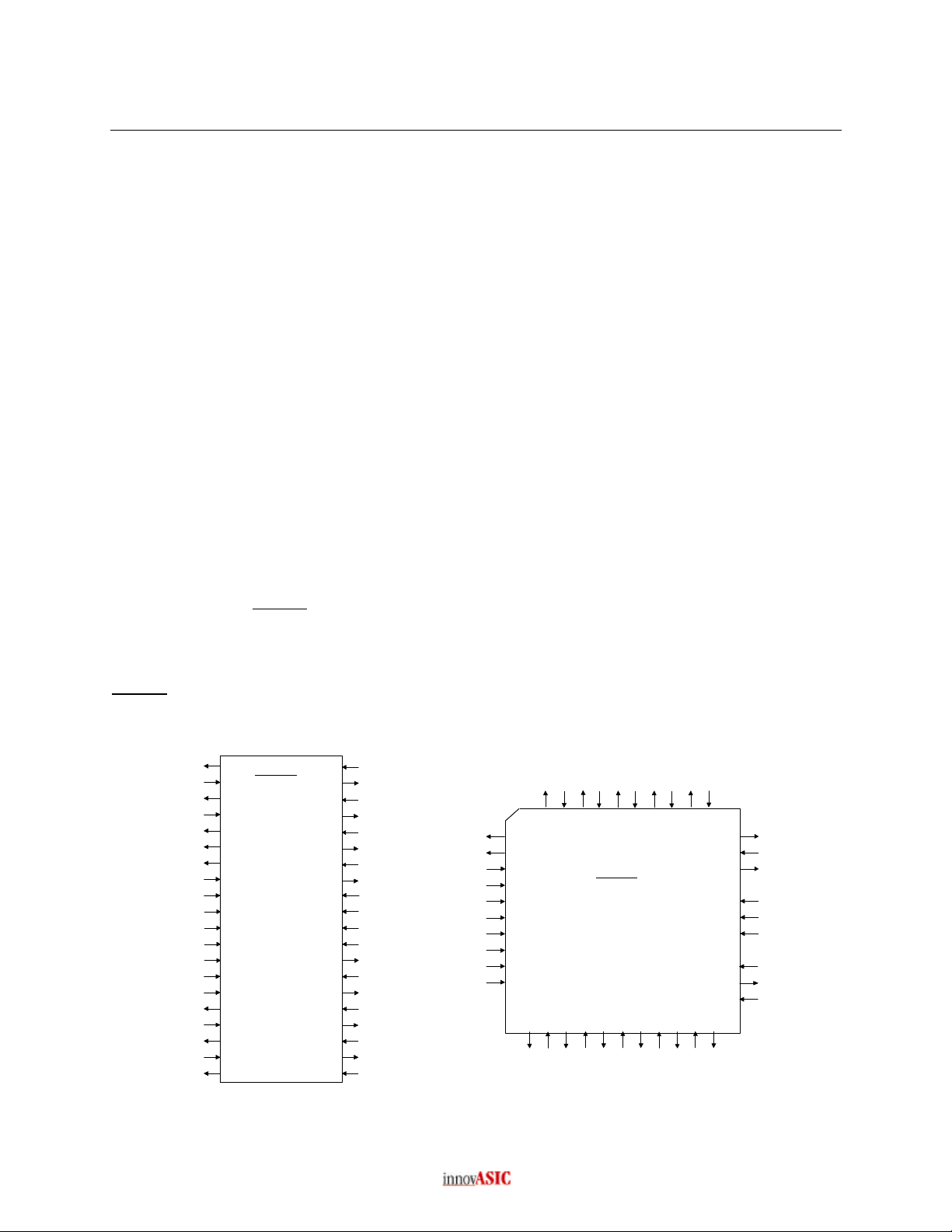
CCn
(1)YOUT4
(2)DIN4
(3)YOUT5
(4)DIN5
(5)VECTn
(6)PLn
(7)MAPn
(8)I3
(9)I2
(10)VCC
(11)I1
(12)I0
(13)CCENn
(14)
(15)RLDn
(16)FULLn
(17)DIN6
(18)YOUT6
(19)DIN7
(20)YOUT7
IA2910A
40 Pin DIP
(40)
(39)
(38)
(37)
(36)
(35)
(34)
(33)
(32)
(31)
(30)
(29)
(28)
(27)
(26)
(25)
(24)
(23)
(22)
(21)
DIN3
YOUT3
DIN2
YOUT2
DIN1
YOUT1
DIN0
YOUT0
CIN
CLK
VDD
OEn
YOUT11
DIN11
YOUT10
DIN10
YOUT9
DIN9
YOUT8
DIN8
DIN5
YOUT5
VECTn
N. C.
(6)
(5)
(4)
(19)
DIN6
(3)
(20)
YOUT6
44 Pin LCC
(21)
DIN7
(7)PLn
(8)MAPn
(9)I3
(10)I2
(11)VCC
(12)I1
(13)I0
(14)CCENn
(15)CCn
(16)RLDn
(17)N.C.
(18)
FULLn
DIN4
YOUT4
(2)
(1)
IA2910A
(22)
YOUT7
(23)
DIN8
DIN3
(44)
(24)
YOUT8
YOUT3
(43)
(25)
DIN9
(42) DIN2
(26)
YOUT9
(41) YOUT2
(27)
DIN10
(40) DIN1
(39)
(38)
(37)
(36)
(35)
(34)
(33)
(32)
(31)
(30)
(29)
(28)
YOUT10
YOUT1
DIN0
YOUT0
N. C.
CIN
CLK
VDD
N. C.
OEn
YOUT11
DIN11
Copyright 1999, InnovASIC Inc.
Customer Specific IC Solutions
Page 2
Page 2 of 19
IA2910A Preliminary Data Sheet
Microprogram Controller
The IA2910A is a form, fit and function compatible part to the AMD 2910A microprogram
controller. The IA2910A is an address controller which will sequence through a series of
microinstructions contained in a ROM or PROM. There are four sources of addresses from which
the IA2910A may select. The first is a direct data bus (DIN) input, which is straightforward. The
second is an internal address register. This register contains data loaded during a previous
microinstruction. The third source is a program counter register, which generally contains the
previous address incremented by one. The final source of addresses is a nine word deep stack
register which gives the capability to execute nested subroutine linkages. All internal registers are
clocked on the rising edge of the clock input (CLK). An OEn input enables the YOUT output bus
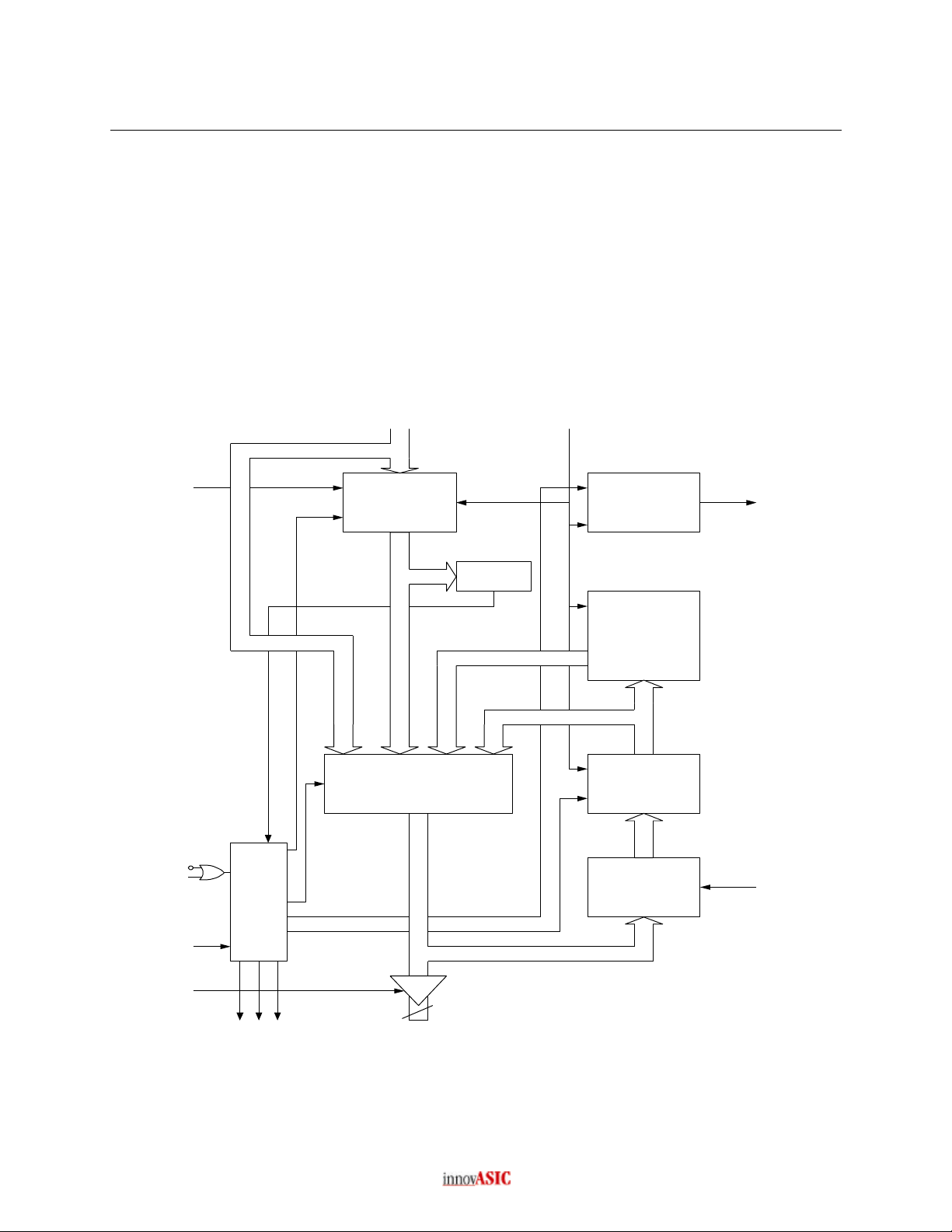
to be tri-stated. A block diagram is shown in Figure 1.
Functional Block Diagram
Figure 1
DIN
CLK
RLDn
CCn
CCENn
Instruction
PLA
R=0
HOLD/LOAD
DECREMENT/
SELECT
PUSH/POP/
HOLD/CLEAR
Register/Counter
Mux
Zero
Detector
Stack Pointer
9 word X 12 Bit
Stack
Microprogram
counter-register
Incrementer
FULLn
CIN
I(3:0)
PLn
MAPn
CLEAR/COUNT
12
YOUT
VECTn
Copyright 1999, InnovASIC Inc.
Customer Specific IC Solutions
Page 3

Page 3 of 19
IA2910A Preliminary Data Sheet
Microprogram Controller
Functional Overview
The IA2910A is a 0.8 µm CMOS microprogram controller intended for use in high-speed
microprocessor applications. It allows addressing of up to 4K words of microprogram.
The controller contains a four-input mux that is used to select either the register/counter, direct
data input, microprogram counter, or stack as the source of the next microinstruction address.
The register/counter consists of 12 D-type, edge-triggered flip-flops, with a common clock enable.
When its load control, RLDn, is LOW, new data is loaded on a positive clock transition. A few
instructions include load; in most systems, these instructions will be sufficient, simplifying the
microcode. The output of the register/counter is available to the mux as a source for the next
microinstruction address. The direct input furnishes a source of data for loading the
register/counter.
The IA2910A contains a microprogram counter that is composed of a 12-bit incrementer followed
by a 12-bit register. The counter can be used in either of two ways. When the carry-in to the
incrementer is HIGH, the microprogram register is loaded on the next clock cycle with the current
YOUT output word plus one. Sequential microinstructions are thus executed. When the carry-in is
LOW, the incrementer passes the YOUT output word unmodified so that the counter is reloaded
with the same YOUT word on the next clock cycle. The same microinstruction is thus executed
any number of times.
The third source for the mux is the direct DIN input. This source is used for branching.
The fourth source available at the mux input is a 9-word by 12-bit stack (file). The stack is used to
provide return address linkage when executing microsubroutines or loops. The stack contains a
built-in stack pointer (SP) which always points to the last file word written. This allows stack
reference operations (looping) to be performed without a pop.
The stack pointer operates as an up/down counter. During microinstructions 1, 4, and 5, the
PUSH operation may occur. This causes the stack pointer to increment and the file to be written
with the required return linkage. On the cycle following the PUSH, the return data is at the new
location pointed to by the stack pointer.
During five microinstructions, a POP operation may occur. The stack pointer decrements at the
next rising clock edge following a POP, effectively removing old information from the top of the
stack.
The stack pointer linkage is such that any sequence of pushes, pops, or stack references can be
achieved. At RESET (Instruction 0), the depth of nesting becomes zero. For each PUSH, the
nesting depth increases by one; for each POP, the depth decreases by one. The depth can grow to
nine. After a depth of nine is reached, FULLn goes LOW. Any further PUSHes onto a full stack
overwrite information at the top of the stack, but leave the stack pointer unchanged. This
operation will usually destroy useful information and is normally avoided. A POP from an empty
stack may place non-meaningful data on the YOUT outputs, but is otherwise safe. The stack
Copyright 1999, InnovASIC Inc.
Customer Specific IC Solutions
Page 4

Page 4 of 19
IA2910A Preliminary Data Sheet
Microprogram Controller
pointer remains at zero whenever a POP is attempted from a stack already empty.
The register/counter is operated during three microinstructions (8, 9, and 15) as a 12-bit down
counter, with result = zero available as a microinstruction branch test criterion. This provides
efficient iteration of microinstructions. The register/counter is arranged such that if it is preloaded
with a number N and then used as a loop termination counter, the sequence will be executed
exactly N + 1 times. During instruction 15, a three-way branch under combined control of the
loop counter and the condition code is available.
The device provides three-state YOUT outputs. These can be particularly useful in designs
requiring automatic checkout of the processor. The microprogram controller outputs can be
forced into the high-impedance state, and pre-programmed sequences of microinstructions can be
executed via external access to the address lines.
Copyright 1999, InnovASIC Inc.
Customer Specific IC Solutions
Page 5

Page 5 of 19
IA2910A Preliminary Data Sheet
Microprogram Controller
I/O Signal Description
Table 1 below describes the I/O characteristics for each signal on the IC. The signal names
correspond to the signal names on the pinout diagrams provided.
Table 1
Symbol Type Description
CLK I Clock Input - Clock source for address register, microprogram
counter register, and stack file.
I(3:0) I Active high instruction bits. Selects instruction to be executed by the
IA2910A.
CCn
I Active low. Condition code. Used as test criterion, pass is low on
CCn.
CCENn I Active low. Condition code enable. When set high, CCn is ignored
and the IA2910A operates as it CCn were a low.
RLDn I Active low. Clock enable to address register, allows loading of
register/counter regardless of instruction or condition.
OEn I Active low. Output enable, when high tri-states the output bus
YOUT.
CIN I Active high. Carry in signal to the incrementer.
FULLn O Active low. Indicates there are nine items on the stack.
DIN(11:0) I Active high. Data bus input to the multiplexer.
YOUT(11:0) O Active high. Data bus output from the IA2910A.
PLn O Active low. Pipeline address enable. Selects source number one
(usually pipeline register) as direct input source.
MAPn O Active low. Map address enable. Selects source number two (usually
mapping PROM or PLA) as direct input source.
VECTn O Active low. Vector address enable. Selects source number three
(usually interrupt starting address) as direct input source.
Theory of Operation
Table 2 shows the result of each instruction in controlling the mux which determines the YOUT
outputs, and in controlling the three enable signals PLn, MAPn, and VECTn. The effect on the
register/counter and the stack after the next positive-going clock edge is also shown. The mux
determines which internal source drives the YOUT outputs. The value loaded into the counter is
Copyright 1999, InnovASIC Inc.
Customer Specific IC Solutions
Page 6

Page 6 of 19
IA2910A Preliminary Data Sheet
Microprogram Controller
either identical to the YOUT output, or else one greater, as determined by CIn. For each
instruction, one and only one of the three outputs PLn, MAPn, and VECTn is LOW. If these
outputs control three-state enables for the primary source of microprogram jumps (usually part of a
pipeline register), a PROM which maps the instruction to a microinstruction starting location, and
an optional third source (often a vector from a DMA or interrupt source), respectively, the threestate sources can drive the DIN inputs without further logic.
Several inputs, as shown in Table 2, can modify instruction execution. The combination CCn
HIGH and CCENn LOW is used as a test in 9 of the 16 instructions. RLDn, when LOW, causes
the DIN input to be loaded into the register/counter, overriding any HOLD or DEC operation
specified in the instruction. OEn, normally LOW, may be forced HIGH to remove the IA2910A
YOUT outputs from a three-state bus.
The stack, a nine-word last-in, first-out 12-bit memory, has a pointer which addresses the value
presently on the top of the stack. Explicit control of the stack pointer occurs during instruction 0
(RESET), which makes the stack empty by resetting the SP to zero. After a RESET, and
whenever else the stack is empty, the contents of the top of stack is undefined until a PUSH occurs.
Any POPs performed while the stack is empty put undefined data on the F outputs and leave the
stack pointer at zero.
Any time the stack is full (nine more PUSHes than POPs have occurred since the stack was last
empty), the FULLn warning output occurs. This signal first appears on the microcycle after a ninth
PUSH. No additional PUSH should be attempted onto a full stack; if tried, information within the
stack will be overwritten and lost.
Copyright 1999, InnovASIC Inc.
Customer Specific IC Solutions
Page 7

Page 7 of 19
IA2910A Preliminary Data Sheet
Microprogram Controller
Instruction Set Description
Table 2
I(3:0) Mnemonic Name Reg/cntr
contents
0 JZ Jump Zero X 0 CLEAR 0 CLEAR HOLD PL
1 CJS Cond JSB PL X PC HOLD D PUSH HOLD PL
2 JMAP Jump Map X D HOLD D HOLD HOLD MAP
3 CJP Cond Jump PL X PC HOLD D HOLD HOLD PL
4 PUSH Push/cond LD
cntr
5 JSRP Cond JSB R/PL X R PUSH D PUSH HOLD PL
6 CJV Cond Jump
Vector
7 JRP Cond Jump
R/PL
8 RFCT Repeat Loop,
Cntr .NE. 0
9 RPCT Repeat PL, cntr
.NE. 0
10 CRTN Cond RTN X PC HOLD F POP HOLD PL
11 CJPP Cond Jump PL
& POP
12 LDCT LD Cntr &
Continue
13 LOOP Test End Loop X F HOLD PC POP HOLD PL
14 CONT Continue X PC HOLD PC HOLD HOLD PL
15 TWB Three-Way
Branch
X PC PUSH PC PUSH NOTE 1 PL
X PC HOLD D HOLD HOLD VECT
X R HOLD D HOLD HOLD PL
.NE. 0
= 0
.NE. 0
= 0
X PC HOLD D POP HOLD PL
X PC HOLD PC HOLD LOAD PL
.NE. 0
= 0
Fail
Y
F
PC
D
PC
F
D
Fail
Stack
HOLD
POP
HOLD
HOLD
HOLD
POP
Pass
Y
F
PC
D
PC
PC
PC
Pass
Stack
HOLD
POP
HOLD
HOLD
POP
POP
Reg/cntr Enable
DEC
HOLD
DEC
HOLD
DEC
HOLD
PL
PL
PL
PL
PL
PL
NOTE 1: If CCENn is LOW and CCn is HIGH, HOLD; ELSE LOAD.
X = Don’t Care
.NE. = Not equal
IA2910A Instruction Set
The IA2910A provides sixteen instructions which select the address of the next microinstruction to
be executed. Four of the instructions are unconditional – their effect depends only on the
instruction. Ten of the instructions have an effect which is partially controlled by an external, datadependent condition. Three of the instructions have an effect which is partially controlled by the
contents of the internal register/counter. The instruction set is shown in Table 2. Examples of the
Instruction Execution are illustrated in Figure 2. In this discussion it is assumed that CIN is tied
HIGH.
In the ten conditional instructions, the result of the data-dependent test is applied to CCn. If the
CCn input is LOW, the test is considered to have been passed, and the action specified in the name
occurs; otherwise, the test has failed and an alternate (often simply the execution of the next
sequential microinstruction) occurs. Testing of CCn may be disabled for a specific microinstruction
by setting CCENn HIGH, which unconditionally forces the action specified in the name; that is, it
forces a pass. Other ways of using CCENn include (1) tying it HIGH, which is useful if no
microinstruction is data-dependent; (2) tying it LOW if data-dependent instructions are never
Copyright 1999, InnovASIC Inc.
Customer Specific IC Solutions
Page 8

Page 8 of 19
IA2910A Preliminary Data Sheet
Microprogram Controller
forced unconditionally; or (3) tying it to the source of IA2910A instruction bit I(0), which leaves
instructions 4, 6, and 10 as data-dependent but makes others unconditional. All of these tricks save
one bit of microcode width.
The effect of three instructions depends on the contents of the register/counter. Unless the
counter holds a value of zero, it is decremented; if it does hold zero, it is held and a different
microprogram next address is selected. These instructions are useful for executing a
microinstruction loop a known number of times. Instruction 15 is affected both by the external
condition code and the internal register/counter.
Instruction 0 JZ JUMP and ZERO, or RESET unconditionally specifies that the address of the
next microinstruction is zero. Many designs use this feature for power-up sequences and provide
the power-up firmware beginning at microprogram memory word location 0.
Instruction 1 CJS is a CONDITIONAL JUMP-TO-SUBROUTINE via the address provided in
the pipeline register. As shown in Figure II, the machine might have executed words at address 50,
51, and 52. When the contents of address 52 is in the pipeline register, the next address control
function is the CJS. Here, if the test is passed, the next instruction executed will be the contents of
microprogram memory location 90. If the test has failed, the CJS will not be executed; the contents
of microprogram memory location 53 will be executed instead. Thus the CJS instruction at location
52 will cause the instruction either in location 90 or location 53 to be executed next. If the TEST
input is such that location 90 is selected, value 53 will be pushed onto the internal stack. This
provides the return linkage for the machine when the subroutine beginning at location 90 is
completed. In this example, the subroutine was completed at location 93 and a RETURN-FROMSUBOUTINE would be found at location 93.
Instruction 2 JMAP is the JUMP MAP instruction. This is an unconditional instruction which
causes the MAPn output to be enabled so that the next microinstruction location is determined by
the address supplied via the mapping PROMs. Normally, the JMAP instruction is used at the end
of the instruction fetch sequence for the machine. In the example of Figure II, microinstructions at
locations 50, 51, 52, and 53 might have been the fetch sequence and at its completion at location 53,
the JMAP function would be contained in the pipeline register. This example shows the mapping
PROM outputs to be 90; therefore, an unconditional jump to microprogram memory address 90 is
performed.
Instruction 3 CJP, CONDITIONAL JUMP PIPELINE, derives its branch address from the
pipeline register branch address value (BR(0) – BR(11) in FIGURE II). This instruction provides a
technique for branching to various microprogram sequences depending upon the test condition
inputs. Quite often, state machines are designed which simply execute tests on various inputs
waiting for the condition to come true. When the true condition is reached, the machine then
branches and executes a set of microinstructions to perform some function. This usually has the
effect of resetting the input being tested until some point in the future. Figure II shows the
conditional jump via the pipeline register address at location 52. When the contents of
microprogram memory word 52 are in the pipeline register, the next address will be either location
53 or location 30 in this example. If the test is passed, the value currently in the pipeline register
(30) will be contained in the microprogram counter which, in this example, is 53.
Copyright 1999, InnovASIC Inc.
Customer Specific IC Solutions
Page 9

Page 9 of 19
IA2910A Preliminary Data Sheet
Microprogram Controller
Instruction 4 PUSH is the PUSH/CONDITIONAL LOAD COUNTER instruction and is used
primarily for setting up loops in microprogram firmware. In Figure II, when instruction 52 is in the
pipeline register, a PUSH will be made onto the stack and the counter will be loaded based on the
condition. When a PUSH occurs, the value pushed is always the next sequential instruction address.
In this case, the address is 53. If the test fails, the counter is not loaded; if it is passed, the counter
is loaded with the value contained in the pipeline register branch address field. Thus, a single
microinstruction can be used to set up a loop to be executed a specific number of times.
Instruction 8 will describe how to use the pushed value and the register/counter for looping.
Instruction 5 JSRP is a CONDITIONAL JUMP-TO-SUBROUTINE via the register/counter or
the contents of the PIPELINE register. As shown in Figure II, a PUSH is always performed and
one of two subroutines executed. In this example, either the subroutine beginning at address 80 or
the subroutine beginning at address 90 will be performed. A return-from-subroutine (instruction
10) returns the microprogram flow to address 55. In order for this microinstruction control
sequence to operate correctly, both the next address fields of instruction 53 and 54 would have to
contain the proper value. Let’s assume that the branch address fields of instruction 53 contain the
value 90 so that it will be in the IA2910A register/counter when the contents of address 54 are in
the pipeline register. This requires that the instruction at address 53 load the register/counter.
Now, during the execution of instruction 5 (at address 54), if the test failed, the contents of the
register (value = 90) will select the address of the next microinstruction. If the test input passes, the
pipeline register contents (value = 80) will determine the address of the next microinstruction.
Therefore, this instruction provides the ability to select one of two subroutines to be executed
based on a test condition.
Instruction 6 CJV is a CONDITIONAL JUMP VECTOR instruction which provides the
capability to take the branch address from a third source heretofore not discussed. In order for this
instruction to be useful, the IA2910A output, VECTn is used to control a three-state control input
of a register, buffer, or PROM containing the next microprogram address. This instruction
provides one technique for performing interrupt type branching at the microprogram level. Since
this instruction is conditional, a pass causes the next address to be taken from the vector source,
while failure causes the next address to be taken from the microprogram counter. In the example
of Figure II, if the CJV instruction is contained at location 52, execution will continue at vector
address 20 if the CCn input is LOW and the microinstruction at address 53 will be executed if the
CCn input is HIGH.
Instruction 7 JRP is a CONDITIONAL JUMP via the contents of the IA2910A register/counter
or the contents of the pipeline register. This instruction is very similar to instruction 5; the
conditional jump-to-subroutine via R or PL. The major difference between instruction 5 and
instruction 7 is that no push onto the stack is performed with 7. Figure II depicts this instruction
as a branch to one of two locations depending on the test condition. the example assumes the
pipeline register contains the value 70 when the contents of address 52 is being executed. As the
contents of address 53 is clocked into the pipeline register, the value 70 is loaded into the
register/counter in the IA2910A. The value 80 is available when the contents of address 53 is in the
pipeline register. Thus, control is transferred to either address 70 or address 80 depending on the
test condition.
Copyright 1999, InnovASIC Inc.
Customer Specific IC Solutions
Page 10

Page 10 of 19
IA2910A Preliminary Data Sheet
Microprogram Controller
Instruction 8 RFCT is the REPEAT LOOP, COUNTER NOT EQUAL ZERO instruction.
This microinstruction makes use of the decrementing capability of the register/counter. To be
useful, some previous instruction, such as 4, must have loaded a count value into the
register/counter. This instruction checks to see whether the register/counter contains a non-zero
value. If so, the register/counter is decremented, and the address of the next microinstruction is
taken from the top of the stack. If the register counter contains zero, the loop exit condition is
occurring; control falls through to the next sequential microinstruction by selecting uPC; the stack
is POP’d by decrementing the stack pointer, but the contents of the top of the stack are thrown
away.
An example of the RFCT instruction is shown in Figure II. In this example, location 50 most likely
would contain a PUSH/CONDITIONAL LOAD COUNTER instruction which would have
caused address 51 to be PUSHed on the stack and the counter to be loaded with the proper value
for looping the desired number of times.
In this example, since the loop test is made at the end of the instructions to be repeated
(microaddress 54), the proper value to be loaded by the instructions at address 50 is one less than
the desired number of passes through the loop. This method allows a loop to be executed 1 to
4096 times. If it is desired to execute the loop from 0 to 4095 times, the firmware should be
written to make the loop exit test immediately after loop entry.
Instruction 9 RPCT is the REPEAT PIPELINE REGISTER, COUNTER NOT EQUAL
ZERO instruction. This instruction is similar to instruction 8 except that the branch address now
comes from the pipeline register rather than the file. In some cases, this instruction may be
thought of as a one-word file extension; that is, by using this instruction, a loop with the counter
can still be performed when subroutines are nested five deep. This instruction’s operation is very
similar to that of instruction 8. The differences are that on this instruction, a failed test condition
causes the source of the next microinstruction address to be the DIN inputs; and, when the test
condition is passed, this instruction does not perform a POP because the stack is not being used.
In the example of Figure II, the RPCT instruction is instruction 52 and is shown as a single
microinstruction loop. The address in the pipeline register would be 52. Instruction 51 in this
example could be the LOAD COUNTER AND CONTINUE instruction (number 12). While the
example shows a single microinstruction loop, by simply changing the address in a pipeline register,
multi-instruction loops can be performed in this manner for a fixed number of times as determined
by the counter.
Instruction 10 CRTN is the CONDITIONAL RETURN-FROM-SUBROUTINE instruction. As
the name implies, this instruction is used to branch from the subroutine back to the next
microinstruction address following the subroutine call. Since this instruction is conditional, the
return is performed only if the test is passed. If the test is failed, the next sequential
microinstruction is performed. The example in Figure II depicts the use of the CRTN instruction
in both the conditional and the unconditional modes. This example first shows a jump-tosubroutine at instruction location 52 where control is transferred to location 90. At location 93, a
CRTN instruction is performed. If the test is passed, the stack is accessed and the program will
Copyright 1999, InnovASIC Inc.
Customer Specific IC Solutions
Page 11

Page 11 of 19
IA2910A Preliminary Data Sheet
Microprogram Controller
transfer to the next instruction at address 53. If the test is failed, the next microinstruction at
address 94 will be executed. The program will continue to address 97 where the subroutine is
complete. To perform an unconditional RETURN-FROM-SUBROUTINE, the CRTN instruction
is executed unconditionally; the microinstruction at address 97 is programmed to force CCENn
HIGH, disabling the test and the forced PASS causes an unconditional return.
Instruction 11 CJPP is the CONDITIONAL JUMP PIPELINE register address and POP stack
instruction. This instruction provides another technique for loop termination and stack
maintenance. The example in Figure II shows a loop being performed from address 55 back to
address 51. The instructions at locations 52, 53, and 54 are all conditional JUMP and POP
instructions. At address 52, if the CCn input is LOW, a branch will be made to address 70 and the
stack will be properly maintained via a POP. Should the test fail, the instruction at location 53 (the
next sequential instruction) will be executed. Likewise, at address 53, either the instruction at 90 or
54 will be subsequently executed, respective to the test being passed or failed. The instruction at 54
follows the same rules, going to either 80 or 55. An instruction sequence as described here, using
the CJPP instruction, is very useful when several inputs are being tested and the microprogram is
looping waiting for any of the inputs being tested to occur before proceeding to another sequence
of instructions. This provides the powerful jump-table programming technique at the firmware
level.
Instruction 12 LDCT is the LOAD COUNTER AND CONTINUE instruction, which simply
enables the counter to be loaded with the value at its parallel inputs. These inputs are normally
connected to the pipeline branch address field which (in the architecture being described here)
serves to supply either a branch address or a counter value depending upon the microinstruction
being executed. There are altogether three ways of loading the counter – the explicit load by this
instruction 12; the conditional load included as part of instruction 4; and the use of the RLDn input
along with any instruction. The use of RLDn with any instruction overrides any counting or
decrementation specified in the instruction, calling for a load instead. Its use provides additional
microinstruction power, at the expense of one bit of microinstruction width. This instruction 12 is
exactly equivalent to the combination of instruction 14 and RLDn LOW. Its purpose is to provide
a simple capability to load the register/counter in those implementations which do not provide
microprogrammed control for RLDn.
Instruction 13 LOOP is the TEST END-OF-LOOP instruction, which provides the capability of
conditionally exiting a loop at the bottom; that is, this is a conditional instruction that will cause the
microprogram to loop, via the file, if the test is failed else to continue to the next sequential
instruction. The example in Figure II shows the LOOP microinstruction at address 56. If the test
fails, the microprogram will branch to address 52. Address 52 is on the stack because a PUSH
instruction had been executed at address 51. If the test is passed at instruction 56, the loop is
terminated and the next sequential microinstruction at address 57 is executed, which also causes the
stack to be POP’d; thus, accomplishing the required stack maintenance.
Instruction 14 CONT is the CONTINUE instruction, which simply causes the microprogram
counter to increment so that the next sequential microinstruction is executed. This is the simplest
microinstruction of all and should be the default instruction which the firmware requests whenever
there is nothing better to do.
Copyright 1999, InnovASIC Inc.
Customer Specific IC Solutions
Page 12

Page 12 of 19
IA2910A Preliminary Data Sheet
Microprogram Controller
Instruction 15 TWB, THREE-WAY-BRANCH, is the most complex. It provides for testing for
both a data-dependent condition and the counter during one microinstruction and provides for
selecting among one of three microinstruction addresses as the next microinstruction to be
performed. Like instruction 8, a previous instruction will have loaded a count into the
register/counter while pushing a microbranch address onto the stack. Instruction 15 performs a
decrement-and-branch-until-zero function similar to instruction 8. The next address is taken from
the top of the stack until the count reaches zero; then the next address comes from the pipeline
register. The above action continues as long as the test condition fails. If at any execution of
instruction 15 the test condition is passed, no branch is taken; the microprogram counter register
furnishes the next address. When the loop is ended, either by the count becoming zero, or by
passing the conditional test, the stack is POP’d by decrementing the stack pointer, since interest in
the value contained at the top of the stack is then complete.
As one example, consider the case of a memory search instruction. As shown in Figure II, the
instruction at microprogram address 63 can be Instruction 4 (PUSH), which will push the value 64
onto the microprogram stack and load the number N, which is one less than the number of
memory locations to be searched before giving up. Location 64 contains a microinstruction which
fetches the next operand from the memory area to be searched and compares it with the search
key. Location 65 contains a microinstruction which tests the result of the comparison and also is a
TWB for microprogram control. If no match is found, the test fails and the microprogram goes
back to location 64 for the next operand address. When the count becomes zero, the
microprogram branches to location 72, which does whatever is necessary if no match is found. If a
match occurs on any execution of the TWB at location 65, control falls through to location 66
which handles this case. Whether the instruction ends by finding a match or not, the stack will
have been POP’d once, removing the value 64 from the top of the stack.
Copyright 1999, InnovASIC Inc.
Customer Specific IC Solutions
Page 13

Page 13 of 19
IA2910A Preliminary Data Sheet
Microprogram Controller
Absolute Maximum Ratings
PARAMETER Min Max UNITS Notes
Supply voltage, V
Input voltage, V
Input Pin Current I
DD
IN
IN
Operating temperature
range
Storage temperature range TBD
Ambient Temperature, T
a
TBD V
TBD V
TBD mA
TBD
°C
°C
TBD
°C
Lead Temperature TBD
°C
Power Dissipation mW
Stresses beyond those listed under “absolute maximum ratings” may cause permanent damage to the
device. Operating the device beyond the conditions indicated in the “recommended operating conditions”
section is not recommended. Operation at the “absolute maximum ratings” may adversely affect device
reliability.
DC Characteristics
PARAMETER Min Max UNITS Notes
DC Supply voltage, V
DD
Static Supply Current, I
Power Supply Current, I
Standby Supply Current, I
Input Capacitance, C
I/O Capacitance, C
Circuit Ground, V
Notes:
IN
I/O
SS
DD
DD
stby
4.5 5.5 V
TBD
µA
TBD mA/MHz
TBD µA
TBD pF
TBD pF
TBD V
(1)
(1) Static IDD current is exclusive of input/output drive requirements and is measured with the clocks
stopped and all inputs tied to VDD or VSS, configured to draw minimum current.
Copyright 1999, InnovASIC Inc.
Customer Specific IC Solutions
Page 14

Page 14 of 19
IA2910A Preliminary Data Sheet
Microprogram Controller
Parametric Voltage and Current Levels (Ambient Temperature = -40 to 85 C)
Input Pin V
IL
V
IH
Hysteresis Note
TBD
Output Pin V
OL
V
OH
I
OL
I
OH
Min Max
TBD
Pullup Pin IPU Note
Min Max
TBD
AC Specifications
Parameter Min Max Notes
TBD
I
OZ
Note
Copyright 1999, InnovASIC Inc.
Customer Specific IC Solutions
Page 15

Page 15 of 19
IA2910A Preliminary Data Sheet
Microprogram Controller
IA2910A Execution Examples
Figure 2
0
1
2
50
51
52
53
7 COND JUMP R/PL
50
51
52
53
70
71
STACK
53
50
51
52
53
54
55
STACK
53
REGISTER/
COUNTER
N
8 REPEAT LOOP, CNTR .NE. 0
80
81
90
91
92
93
94
95
96
97
13 TEST END LOOP
50
51
52
53
54
55
56
57
11 COND JUMP PL & POP10 COND RETURN
50
51
52
53
54
55
90
91
92
93
94
50
51
52
53
54
55
50
51
52
53
54
55
56
STACK PUSH
52
STACK
53
90
91
92
93
50
51
52
53
54
55
56
57
STACK PUSH
STACK PUSH
51
REGISTER/
COUNTER
N
51
80
81
82
50
51
52
53 90
STACK
55
80
81
82
83
84
9 REPEAT PL, CNTR .NE. 0
90
91
92
14 CONTINUE
50
51
6 COND JUMP VECTOR5 COND JSB R/PL4 PUSH/COND LD CNTR
50
51
52
53
54
50
51
52
53
70
71
72
3 COND JUMP PL2 JUMP MAP1 COND JSB PL0 JUMP ZERO
50
51
52
53
91
12 LD CNTR & CONTINUE
COUNTER
(LDCT)
N
50
51
52
53
54
20
21
15 THREE-WAY BRANCH
62
63
64
65
66
COUNTER
N
STACK PUSH
64
REGISTER/
COUNTER
N
72
73
30
31
Copyright 1999, InnovASIC Inc.
Customer Specific IC Solutions
Page 16

Page 16 of 19
A
D
IA2910A Preliminary Data Sheet
Microprogram Controller
PLCC Packaging Dimensions (Theta J = TBD)
PIN 1
IDENTIFIER & ZONE
E
E1
D1
A1
.030 ± .005
e
D2 / E2
TOP VIEW
.013/.021
SEATING PLANE
.020 MIN.
R 70 ± 2 Deg.
.03R
BOTTOM VIEW
LEAD COUNT
44 (in Inches)
Symbol
A .150 .154
A1 .0007 .0103
D1 .652 .656
D2 .610 .630
E1 .652 .656
E2 .610 .630
e .050 ± .002
D .685 .695
E .685 .695
MIN MAX
SIDE VIEW
Copyright 1999, InnovASIC Inc.
Customer Specific IC Solutions
Page 17

Page 17 of 19
TOP
IA2910A Preliminary Data Sheet
Microprogram Controller
PDIP Packaging Dimensions (Theta J = TBD)
E1
E
LEAD 1
IDENTIFIER
1
LEAD COUNT
DIRECTION
eA
eB
SIDE VIEW (WIDTH)
C
Lead Count
D
Symbol
A - .220
A1 .015 -
A2
A
A1
L
B
B1
e
SIDE VIEW (LENGTH)
B .016 -
B1 .040 -
C - D 2.045 2.055
E .600 .620
E1 .545 .555
e .700 TYP
eA .620 eB - .660
28 (in Inches)
MIN MAX
L .125 TYP
Copyright 1999, InnovASIC Inc.
Customer Specific IC Solutions
Page 18

Page 18 of 19
IA2910A Preliminary Data Sheet
Microprogram Controller
Package Options
The IA2910A is available in two package styles as shown in the table below.
Package Type Environment Order Number
40 Lead Ceramic DIP, 600 mil wide Military IA2910A-CD40M
Industrial IA2910A-PDW40I40 Lead Plastic DIP, 600 mil wide
Commercial IA2910A-PDW40C
44 Lead Ceramic Leaded Chip Carrier Military IA2910A-CLC44M
44 Lead Ceramic Leadless Chip Carrier Military IA2910A-CLL44M
Industrial IA2910A-PLC44I44 Lead Plastic Leaded Chip Carrier
Commercial IA2910A-PLC44C
The following diagram depicts the innovASIC Product Identification Number.
IAXXXXX-PPPPNNNT/SP
Special Processing:
S = Space
Q = MIL-STD-883
Temperature:
C = Commercial
I = Industrial
M = Military
Number of Leads
Package Type:
Per Package Designator Table
IC Base Number
innovASIC Designator
Copyright 1999, InnovASIC Inc.
Customer Specific IC Solutions
Page 19

Page 19 of 19
IA2910A Preliminary Data Sheet
Microprogram Controller
Package Designator Table
Package Type
innovASIC
Designator
Ceramic side brazed Dual In-line CDB
Cerdip with window CDW
Ceramic leaded chip carrier CLC
Cerdip without window CD
Ceramic leadless chip carrier CLL
PLCC PLC
Plastic DIP standard (300 mil) PD
Plastic DIP standard (600 mil) PDW
Plastic metric quad flat pack PQF
Plastic thin quad flat pack PTQ
Skinny Cerdip CDS
Small outline plastic gull-wing(150 mil body) PSO
Small outline medium plastic gull-wing (207 mil body) PSM
Small outline narrow plastic gull wing (150 mil body) PSN
Small outline wide plastic gull wing (300 mil body) PSW
Skinny Plastic Dip PDS
Shrink small outline plastic (5.3mm .208 body) PS
Thin shrink small outline plastic PTS
Small outline large plastic gull wing (330 mil body) PSL
Thin small outline plastic gull-wing (8 x 20mm) [TSOP] PST
PGA CPGA
BGA CBGA
Contact innovASIC for other package and processing options.
Copyright 1999, InnovASIC Inc.
Customer Specific IC Solutions
 Loading...