

Page 1

IA21140AF Preliminary Data Sheet
ASIC
PCI FAST ETHERNET LAN CONTROLLER
innov
Features
• Form, Fit and Function Compatible with the DEC 21140AF
• Available in 144 Pin PQFP Package
• Integrated Ethernet controller with PCI bus interface
• Supports 10 Mb/s and 10/100 Mb/s network interface
• PCS and scrambler/descrambler circuitry on chip
• Supports multiple PCI features:
- Unlimited PCI burst
- PCI read multiple
- PCI write and invalidate
- PCI read line
- PCI 5.0V and 3.3V environments
• Multiple interrupt sources
• Contains two independent 3K FIFOs to minimize external memory additions
• Provides sleep or snooze low-power modes
• Interfaces with MicroWire Serial ROM
• Provides a JTAG test port with boundary scan function
• Complies with IEEE 802.3, ANSI 8802-3, and Ethernet standards
The IA21140AF is a "plug -and-play" drop-in replacement for the original IC. innovASIC produces
replacement ICs using its MILESTM, or Managed IC Lifetime Extension System, cloning technology. This
technology produces replacement ICs far more complex than "emulation" while ensuring they are compatible
with the origina l IC. MILESTM captures the design of a clone so it can be produced even as silicon
technology advances. MILESTM also verifies the clone against the original IC so that even the
"undocumented features" are duplicated. This data sheet documents all necessary engineering information
about the IA21140AF including functional and I/O descriptions, electrical characteristics, and applicable
timing.
Copyright 2001 ENG210010110-00 www.innovasic.com
innovASIC Customer Support:
The End of Obsolescence Page 1 of 19 1-888-824-4184
Page 2

IA21140AF Preliminary Data Sheet
PCI FAST ETHERNET LAN CONTROLLER
Package Pinout
tdi
tms
tck
srl_txen
srl_tclk
srl_txd
srl_rxen
srl_rxd
srl_clsn
mii_srl
sym_txd[4]
vdd
vss
mii_sym_txd[3]
mii_sym_txd[2]
1
1
1
1
1
1
1
1
3
3
3
3
2
3
4
5
2
2
3
3
8
9
0
1
IA21140AF
mii_sym_txen
mii_sym_txd[1]
mii_sym_txd[0]
sym_link
mii_sym_tclk
1
1
1
1
1
2
7
2
2
2
2
3
4
5
6
rcv_match
vdd
vss
1
1
1
2
2
2
0
1
2
sym_rxd[4]
mii_sym_rxd[3]
mii_sym_rxd[2]
mii_sym_rxd[1]
1
1
1
1
1
1
1
1
6
7
8
9
mii_sym_rxd[0]
mii_sym_rclk
mii_crs
mii_clsn
mii_dv
1
1
1
1
1
1
5
1
1
1
1
1
2
3
4
mii_err
1
1
0
1
9
0
2
sd
108
107
106
105
104
103
102
101
100
99
98
97
96
95
94
93
92
91
90
89
88
87
86
85
84
83
82
81
80
79
78
77
76
75
74
73
vss
vdd
mii_mdc
mii_mdio
nc
br_a[1]
br_a[0]
br_ce_n
br_ad[7]
br_ad[6]
vdd
vss
br_ad[5]
br_ad[4]
br_ad[3]
br_ad[2]
br_ad[1]
br_ad[0]
vss
gep[7]
gep[6]
gep[5]
gep[4]
vdd
vss
gep[3]
gep[2]
gep[1]
gep[0]
sr_cs
sr_ck
sr_di
sr_do
vdd
vss
vdd_clamp
int_n
rst_n
vdd
vss
pci_clk
vdd
gnt_n
req_n
vss
ad[31]
ad[30]
vss
ad[29]
ad[28]
vss
ad[27]
ad[26]
vdd
ad[25]
ad[24]
c_be_n[3]
idsel
vss
ad[23]
ad[22]
ad[21]
ad[20]
vdd
ad[19]
ad[18]
vdd
vss
vss
ad[17]
ad[16]
vss
tdo
1
1
1
1
1
4
1
4
2
3
4
5
6
7
8
9
10
11
12
13
14
15
16
17
18
19
20
21
22
23
24
25
26
27
28
29
30
31
32
33
34
35
36
37383940414243444546474849505152535455565758596061626364656667686970717
4
4
4
4
0
1
2
3
srl_rclk
1
1
1
1
3
3
3
3
6
7
8
9
vss
frame_n
c_be_n[2]
irdy_n
trdy_n
stop_n
devsel_n
vdd
serr_n
perr_n
par
vss
c_be_n[1]
ad[15]
ad[14]
vss
ad[13]
ad[12]
ad[11]
vdd
ad[9]
ad[10]
vss
ad[8]
vss
ad[7]
ad[6]
c_be_n[0]
ad[5]
ad[4]
vdd
ad[3]
ad[2]
vss
ad[1]
ad[0]
Copyright 2001 ENG210010110-00 www.innovasic.com
innovASIC Customer Support:
The End of Obsolescence Page 2 of 19 1-888-824-4184
Page 3

IA21140AF Preliminary Data Sheet
PCI FAST ETHERNET LAN CONTROLLER
Description
The innovASIC IA21140AF Fast Ethernet LAN controller provides a direct interface connection to
the PCI (Peripheral Component Interface) bus. It interfaces with the PCI bus by using on-chip
control and status registers (CSR’s), and a shared CPU memory area. The memory is initialized once
during setup to minimize CPU overhead during normal operation. Large receive and transmit
FIFO’s are contained on-chip so no additional on board memory is required. The IA21140AF
includes two on chip direct memory access (DMA) controllers with programmable burst size
providing for low CPU utilization. A PCI clock frequency from dc to 33 MHz (20-33 MHz for
operational network interface) is supported. Two network ports are supported. A serial standard 7wire 10-Mbps port (SRL) and a media independent interface/symbol 10/100-Mbps port
(MII/SYM). The 10 Mbps implements a direct interface to the external 10 Mbps front-end decoder
(ENDEC). The 10/100 Mbps port supports two modes. The first is a 100BASE -X physical coding
sublayer (PCS). The second is a full implementation of the MII standard. The IA21140AF functions
in a full-duplex environment for either network port.
Copyright 2001 ENG210010110-00 www.innovasic.com
innovASIC Customer Support:
The End of Obsolescence Page 3 of 19 1-888-824-4184
Page 4
IA21140AF Preliminary Data Sheet
PCI FAST ETHERNET LAN CONTROLLER
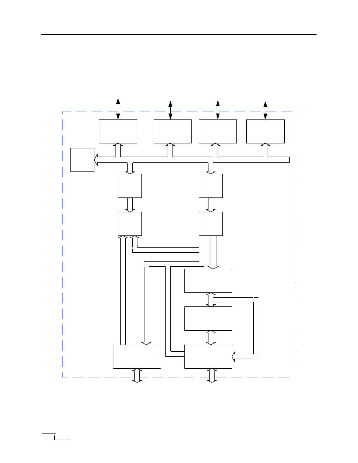
System Block Diagram
This block below illustrates the major functions of the IA21140AF.
Board
Control
Signals
PCI
Boot ROM/
External
Register
Serial
ROM
DMA
PCI
Interface
Rx
FIFO
RxM TxM
Boot
ROM
Port
32
32 32
16 16
4
32 32 8
Physical
Coding
Sublayer
Serial
ROM
Port
Tx
FIFO
General-
Purpose
Register
4
4
1 1
Serial
Interface
10 Mb/s
Copyright 2001 ENG210010110-00 www.innovasic.com
innovASIC Customer Support:
The End of Obsolescence Page 4 of 19 1-888-824-4184
Scrambler/
Descrambler
MII/SYM
Interface
10 Mb/s or 100 Mb/s
4
Page 5

IA21140AF Preliminary Data Sheet
The PCI address and data lines are multiplexed on the same PCI pins. During
the first clock cycle of a transaction, the 32 bits contain an address and during
subsequent clock cycles, they contain data. Both read and write bursts are
operation only. Big or Little Indian byte ordering can be
Address line bit 0 also carries in two consecutive address cycles (bits 16 and
17) in a 256KB configuration. Bit 1 also latches the boot ROM address and
In the first of two consecutive address cycles, these multiplexed lines contain
the boot ROM address bits [7:2], oe_n, and we_n. The second cycle contains
data
e same PCI pins. These
bits provide the bus command during the address phase of the transaction.
They provide the byte enable during the data phase. Byte enable determines
which byte lines carry valid data. Bit 0 coincides with byte 0. Bit 1 coincides
Indicates that the driving device has decoded its address as the target of the
current access. As an input, determines whether a device on the bus has
ndicate the beginning and
duration of a bus transaction access. Data transfer continues while this signal
is asserted. Deasserting this signal indicates the transaction is in the final
m either input or output
Used as a chip select by the host to indicate configuration read and write
e of the appropriate bits in CSR5 gets set, interrupt request gets
asserted if the corresponding mask bit in CSR7 is not set. If more than one
interrupt bit in CSR5 is set and all input bits are not cleared, interrupt request
cycle. Interrupt request gets deasserted by
writing a “1” into the appropriate CSR5 bit. This pin must be pulled up by an
PCI FAST ETHERNET LAN CONTROLLER
I/O Description
The following section provides a functional description of the I/O pins on the IA21140AF.
NAME Type
Vdd P 3.3 volt input supply voltage.
Vdd_clamp P 5.0 volt reference for 5.0 volt signaling environments and 3.3 volt reference
for 3.3 volt signaling environments.
Vss P Ground Pin
ad[31:0] I/O
supported in master
used.
br_a[1:0] O
control lines via two external latches.
br_ad[7:0] I/O
Description
boot ROM address bits [15:8]. Bits 7 through 0 contain data during the
cycle. These lines are used to carry data to and from the external register.
br_ce_n O Enable pin for the Boot ROM or an external register. Pin has an internal 5 k O
pull-up resistor.
c_be_n[3:0] I/O Bus command and byte enable are multiplexed on th
with byte 1, etc.
devsel_n I/O
been selected.
frame_n I/O The IA21140AF bus master asserts this signal to i
phase.
gep[7:0] I/O These pins can be configured by software to perfor
functions for system specific applications.
gnt_n I Indicates to the IA21140AF that access to the bus has been granted.
Idsel I
cycles.
int_n O/D When on
gets deasserted for one clock
external resistor.
Copyright 2001 ENG210010110-00 www.innovasic.com
innovASIC Customer Support:
The End of Obsolescence Page 5 of 19 1-888-824-4184
Page 6

IA21140AF Preliminary Data Sheet
When the IA21140AF is the bus master, this signal is asserted during write
bit ad bus. It is asserted
during read operations to indicate the master is ready to accept data. It is
asserted during a write to indicate that valid data is on the AD lines. A data
ock when both irdy_n and
trdy_n are asserted. Wait cycles are inserted until both these signals are
When an external physical layer protocol (PHY) device detects a collision, it
An external PHY sets this bit when receive data is on the mii_sym_rxd lines
and is cleared at the end of the packet. This signal is synchronized with
or is detected by an external PHY device, this pin
gets set. It is synchronized to mii_sym_rclk and can be set for a minimum of
one receive clock. It sets the cyclic redundancy check (CRC) error bit in the
Goes to the PHY devices as timing reference for the transfer of information
selected. Cleared when the SRL port is
This clock, recovered by the PHY, supports either the 25 MHz or 2.5 MHz
When MII mode is selected, these four parallel data lines receive data that is
n by external PHY that attached the media. Synchronized to the
This 25 MHz or 2.5 MHz transmit clock is supplied by the external physical
These four parallel transmit data lines are synchronized and latched by the
This signal indicates a transmit to an external PHY device. It reflects the
Timing of the PCI related functions is based on this DC to 33 MHz clock. All
bus signals except int_n and rst_n are sampled on the rising edge of this
Used for reporting data parity errors during all PCI transactions except a
When asserted for at least 10 PCI clock cycles, the IA21140AF is reset to its
put pins are tristated and all PCI O/D signals are left
PCI FAST ETHERNET LAN CONTROLLER
NAME Type
irdy_n I/O
operations indicating valid data is present on the 32 -
phase is completed on any rising edge of the cl
asserted together.
mii_clsn I
asserts this signal.
Carrier sense
mii_crs
mii_dv I
mii_err I When a data decoding err
mii_mdc O
mii_mdio I/O Transfers control information and status between the IA21140AF and PHY.
mii_srl O Set when the MII/SYM port is
mii_sym_rclk I
mii_sym_rxd[3:0] I
mii_sym_tclk I
mii_sym_txd[3:0] O
mii_txen O
Nc O No connection pins
Par I/O Even parity bit for the 32-bit ad bus and the 4-bit c_be_n lines. It is driven by
pci_clk I
I The PHY sets this bit when the media is active.
mii_sym_rclk.
receive descriptor (RDES0) when it is set during a packet reception.
on the mii_mdio signal.
selected.
receive clock.
drive
mii_sym_rclk signal.
layer medium dependent device (PMD) and must always be active.
external PHY on the rising edge of the mii_sym_tclk signal.
transmit activity of the MAC sublayer when in the PCS mode (CSR6[23]).
the master for address and write data phases and driven by the target for
read data phases.
Description
clock.
perr_n I/O
special cycle.
rcv_match O Set when a received packet passes address recognition.
req_n O Request to the bus arbiter for the IA21140AF to use the bus.
rst_n I
initial state. PCI out
floating.
sd I Supplied by an external PMD device.
Copyright 2001 ENG210010110-00 www.innovasic.com
innovASIC Customer Support:
The End of Obsolescence Page 6 of 19 1-888-824-4184
Page 7

IA21140AF Preliminary Data Sheet
Reports errors other than parity. Signal must be valid for at least one clock
hernet cable to the IA21140AF.
Asserted and deasserted asynchronously by the external ENDEC with
Carries the recovered receive clock supplied by an external ENDEC. May be
rries the input receive data from the external ENDEC. Incoming data
Set when receive data is present on the Ethernet cable and cleared at the
usly to the receive clock by the
Carries the transmit clock supplied by an external ENDEC. Must be always
Carries the serial output data from the IA21140AF and is synchronized to
The current target is requesting the bus master to stop the current
This signal and the four receive lines mii_sym_rxd[3:0], provide five parallel
data lines in symbol form for use in PCS mode. Data is driven by an external
gnal and the four transmit lines mii_sym_txd[3:0], provide five parallel
data lines in symbol form for use in PCS mode. Data is synchronized on the
data
During JTAG test operations this pin serially shifts test data and instruction
resistor and
During JTAG test operations this pin serially shifts test data and instructions
Controls the state operation of JTAG testing in the IA21140AF. The pin is
Indicates the readiness of the target’s agent to complete the current data
phase of the transaction. During reads, this signal indicates that valid data is
arget is ready to
accept data. A data phase is completed on any clock when both irdy_n and
PCI FAST ETHERNET LAN CONTROLLER
NAME Type
serr_n O/D
cycle. This pin pulled up by an external resistor.
sr_ck O Serial ROM clock.
sr_cs O Serial ROM chip -select pin pulled down by an internal 2 k O resistor.
sr_di O Serial ROM data-in.
sr_do I Serial ROM data-out pin pulled up by an internal 5 k O resistor.
srl_clsn I Indicates a collision occurrence on the Et
respect to the receive clock.
srl_rclk I
inactive during idle periods.
srl_rxd I Ca
should be synchronous with receive clock (srl_rclk) signal.
srl_rxen I
end of a frame. Set and cleared asynchrono
external ENDEC.
srl_tclk I
active, even during reset.
srl_txd O
transmit clock signal.
srl_txen O Signals an external ENDEC that the IA21140AF transmit is in progress.
stop_n I/O
transaction.
sym_link O Descrambler is locked to the input data signal.
sym_rxd[4] I
Description
PMD device and is synchronized with respect to the mii_sym_rclk signal.
sym_txd[4] O This si
rising edge of mii_sym_tclk.
tck I During JTAG test operations this clock shifts state information and test
into and out of the IA21140AF. The pin should not be left unconnected.
Tdi I
into the IA21140AF. The pin is pulled up by an internal 5 k O
should not be left unconnected.
tdo O
out of the IA21140AF.
tms I
pulled up by an internal 5 k O resistor and should not be left unconnected.
trdy_n I/O
present on AD lines. During writes, this signal indicates the t
trdy_n are set.
Copyright 2001 ENG210010110-00 www.innovasic.com
innovASIC Customer Support:
The End of Obsolescence Page 7 of 19 1-888-824-4184
Page 8

IA21140AF Preliminary Data Sheet
PCI FAST ETHERNET LAN CONTROLLER
AC/DC Parameters
DC Characteristics
Absolute Max Ratings
Symbol Parameter Min Max Unit
V
Supply voltage (3.3V) 3 3.6 V
DD
VDD Supply Voltage (5V) 4.75 5.25 V
T
Ambient Temperature (Commercial) 0 70
A
T
Junction Temperature (Commercial) 0 85
J
°C
°C
Storage Temperature -55 125
°C
CMOS Input Specifications (3.0V < VDD < 3.6V; 0 °C < T < 70°C)
Symbol Parameter Min Max Unit
Vil Low level input voltage - 0.3*V
Vih High level input voltage 0.7*V
Lil Low level input current - -1
Iih High level input current - 1
Iil Input pull -up current -27 -75
Iih Input pull -down current 35 112
Vt- Schmitt negative threshold 0.2*V
Vt+ Schmitt positive threshold - 0.8*V
Vh Schmitt hysteresis 0.8 - V
- V
DD
- V
DD
V
DD
V
DD
µA
µA
µA
µA
Copyright 2001 ENG210010110-00 www.innovasic.com
innovASIC Customer Support:
The End of Obsolescence Page 8 of 19 1-888-824-4184
Page 9

IA21140AF Preliminary Data Sheet
PCI FAST ETHERNET LAN CONTROLLER
TTL Input Specifications (3.0V < VDD < 3.6V; 0 °C < T < 70°C)
Symbol Parameter Min Max Unit
Vil Low level input voltage - 0.8 V
Vih High level input voltage 2 - V
Lil Low level input current - -1
Iih High level input current - 1
Iil Input pull -up current -27 -75
Iih Input pull -down current 35 112
Vt- Schmitt negative threshold 0.7 - V
Vt+ Schmitt positive threshold - 2.1 V
Vh Schmitt hysteresis 0.4 - V
µA
µA
µA
µA
Output Operating Specifications (3.0V <VDD <3.6V; 0°C < T < 70°C)
Driver Vol Max
(V)
1 mA Driver 0.4 2.4 1 -1
2 mA Driver 0.4 2.4 2 -2
4 mA Driver 0.4 2.4 4 -4
8 mA Driver 0.4 2.4 8 -8
Voh Min
(V)
Iol Max
(mA)
Ioh Max
(mA)
16 mA Driver 0.4 2.4 16 -16
Copyright 2001 ENG210010110-00 www.innovasic.com
innovASIC Customer Support:
The End of Obsolescence Page 9 of 19 1-888-824-4184
Page 10

IA21140AF Preliminary Data Sheet
PCI FAST ETHERNET LAN CONTROLLER
AC Characteristics
PCI Clock:
Timing Diagram
Thigh
5.0 V Clock
2.0 V
0.8 V
Tr Tf
0.475 * vdd clamp
3.3 V Clock
0.325 * vdd clamp
Tcycle
Tlow
PCI Clock Specification Timing Characteristics
Symbol Parameter Min Max Unit
Tcycle Cycle time 30 50 ns
Thigh pci_clk high time 11 - ns
Tlow pci_clk low time 11 - ns
Tr pci_clk slew rate 1 4 V/ns
Tf pci_clk slew rate 1 4 V/ns
Copyright 2001 ENG210010110-00 www.innovasic.com
innovASIC Customer Support:
The End of Obsolescence Page 10 of 19 1-888-824-4184
Page 11

IA21140AF Preliminary Data Sheet
PCI FAST ETHERNET LAN CONTROLLER
PCI Reset:
Timing Diagram
pci_clk
pci_rst
Internal
Reset
10 pci_clk cycles
33 pci_clk cycles
Timing Characteristics
Symbol Parameter Min Max Conditions
Trst pci_rst pulse width 10 * Tcycle Not applicable pci_clk active
Copyright 2001 ENG210010110-00 www.innovasic.com
innovASIC Customer Support:
The End of Obsolescence Page 11 of 19 1-888-824-4184
Page 12

IA21140AF Preliminary Data Sheet
PCI FAST ETHERNET LAN CONTROLLER
PCI Other Signals:
Timing Diagram
clk
Tval (max) Tval (min)
output
Ton Toff
input
Th
Tsu
Note: Vtest is 1.5 V in a 5.0 V signaling environment and is
0.4 * vdd_clamp in a 3.3 V signaling environment.
Timing Characteristics
Symbol Parameter Min Max Unit
Vtest*
Tval clk-to-signal valid delay 2 11 ns
Ton Float-to-active delay from clk 2 - ns
Toff Active-to-float delay from clk - 28 ns
Tsu Input signal valid setup time before clk 7 - ns
Th Input signal hold time from clk 0 - ns
Copyright 2001 ENG210010110-00 www.innovasic.com
innovASIC Customer Support:
The End of Obsolescence Page 12 of 19 1-888-824-4184
Page 13

IA21140AF Preliminary Data Sheet
PCI FAST ETHERNET LAN CONTROLLER
MII/SYM Port Timing Waveforms:
Transmit:
Timing Diagram
Tcc
Tcr
mii_sym_tclk
Trv
mii_sym_txd[3:0]
mii_sym_txen
Timing Characteristics
Symbol Definition Min* Typ* Max* Units
Tcc
Tch mii_sym_tclk high time 14t - 26t ns
Tcl mii_sym_tclk low time 14t - 26t ns
mii_sym_tclk cycle time (±50 ppm)
Tch
Tcf
Tcl
Trh
- 40t - ns
Tcr mii_sym_tclk rise time - 8 - ns
Tcf mii_sym_tclk fall time - 8 - ns
Trv mii_ tclk rise to mii_txen valid time or
mii_sym_tclk rise to mii_sym_txd valid time
Trh mii_txen hold after mii_tclk rise time 5 - - ns
• t = 1 for 100 Mbps operation and t = 10 for 10 Mbps operation.
- - 20 ns
Copyright 2001 ENG210010110-00 www.innovasic.com
innovASIC Customer Support:
The End of Obsolescence Page 13 of 19 1-888-824-4184
Page 14

IA21140AF Preliminary Data Sheet
PCI FAST ETHERNET LAN CONTROLLER
Receive:
Timing Diagram
Tcc
Tcr
Tch
mii_sym_rclk
Tcf
Tcl
mii_sym_rxd[3:0]
mii_dv
Timing Characteristics
Symbol Definition Min* Typ* Max* Unit
Tcc
Tch mii_sym_rclk high time 14t - 26t ns
Tcl mii_sym_rclk low time 14t - 26t ns
Tcr mii_sym_rclk rise time - 8 - ns
Tcf mii_sym_rclk fall time - 8 - ns
Tts mii_sym_rxd setup (both rise and fall) to
mii_sym_rclk cycle time (±50 ppm)
mii_sym_rclk rise time or mii_dv setup (both rise
and fall) to mii_rclk rise time
Tts
Tth
- 40t - ns
8 - - ns
Tth mii_sym_rxd hold (both rise and fall) after
mii_sym_rclk rise time or mii_dv hold (both rise
and fall) after mii_rclk rise time.
* t = 1 for 100 Mbps operation and t = 10 for 10 Mbps operation.
10 - - ns
Copyright 2001 ENG210010110-00 www.innovasic.com
innovASIC Customer Support:
The End of Obsolescence Page 14 of 19 1-888-824-4184
Page 15

IA21140AF Preliminary Data Sheet
PCI FAST ETHERNET LAN CONTROLLER
Receive Error:
Timing Diagram
mii_rclk
sd
Timing Characteristics
Symbol Definition Min Max Units
Tts mii_err setup (both rise and fall) to mii_rclk rise
time
Tth mii_err hold (both rise and fall) after mii_rclk rise
time.
Collision and Carrier Sense:
Timing Diagram
mii_clsn
mii_crs
Tts
Tth
10 - ns
10 26t ns
Tclh
Timing Characteristics
Symbol Definition Min Max Units
Tclh Mii_crs, mii_clsn high time 20 - ns
Copyright 2001 ENG210010110-00 www.innovasic.com
innovASIC Customer Support:
The End of Obsolescence Page 15 of 19 1-888-824-4184
Page 16

IA21140AF Preliminary Data Sheet
PCI FAST ETHERNET LAN CONTROLLER
Serial Port Timing Waveforms:
Transmit:
Timing Diagram
Ttcf Ttcr
Ttcl Ttch
srl_tclk
Ttcc
Ttdp Ttdh
srl_txd[3:0]
Ttep Tteh
srl_txen
Timing Characteristics
Symbol Definition Min Max units
Ttcl srl_tclk low time 45 55 ns
Ttch srl_tclk high time 45 55 ns
Ttcr srl_tclk rise time - 8 ns
Ttcf srl_tclk fall time - 8 ns
Ttdp srl_tclk fall time to srl_txd valid - 26 ns
Ttdh srl_txd hold after srl_tclk fall time 5 - ns
Ttep srl_tclk fall time to srl_txen valid - 26 ns
Tteh srl_txen hold after srl_tclk fall time 5 - ns
Copyright 2001 ENG210010110-00 www.innovasic.com
innovASIC Customer Support:
The End of Obsolescence Page 16 of 19 1-888-824-4184
Page 17

IA21140AF Preliminary Data Sheet
PCI FAST ETHERNET LAN CONTROLLER
Receive:
Timing Diagram
Start of Packet
srl_rclk
srl_rxd
srl_rxen
End of Packet
srl_rclk
srl_rxd
Bit n-1 Bit n
Trds
Trcc
Trdh
Trcr
Trcl Trch
Trcf
Treh
Trel
srl_rxen
Copyright 2001 ENG210010110-00 www.innovasic.com
innovASIC Customer Support:
The End of Obsolescence Page 17 of 19 1-888-824-4184
Page 18

IA21140AF Preliminary Data Sheet
PCI FAST ETHERNET LAN CONTROLLER
Timing Characteristics
Symbol Definition Min Max Units
Trcc srl_rclk cycle time 85 118 ns
Trcl srl_rclk low time 38 80 ns
Trch srl_rclk high time 38 80 ns
Trcr srl_rclk rise time - 8 ns
Trcf srl_rclk fall time - 8 ns
Trds srl_rxd setup to srl_rclk fall time 10 - ns
Trdh srl_rxd hold after srl_rclk fall time 5 - ns
Trel srl_rxen low time 120 - ns
treh srl_rxen hold after srl_rclk rise time 10 100 ns
Collision:
Timing Diagram
Timing Characteristics
Symbol Definition Min Max Units
Tclh srl_clsn high time 20 - ns
Tclh
srl_clsn
Copyright 2001 ENG210010110-00 www.innovasic.com
innovASIC Customer Support:
The End of Obsolescence Page 18 of 19 1-888-824-4184
Page 19

IA21140AF Preliminary Data Sheet
PCI FAST ETHERNET LAN CONTROLLER
Ordering Information
Order Number Environment Package Type
IA21140AF-PQF144I Industrial 144 Pin Plastic Quad Flat Package
Cross Reference to Original Manufacturer Part Numbers:
innovASIC Part Number DEC Part Number
IA21140AF-PQF144I q 21140-AA
q 21140-AE
q 21140-AF
Copyright 2001 ENG210010110-00 www.innovasic.com
innovASIC Customer Support:
The End of Obsolescence Page 19 of 19 1-888-824-4184
 Loading...