

Datasheet HYM64V8005GU-50, HYM64V8005GU-60, HYM64V8045GU-50, HYM64V8045GU-60, HYM72V8045GU-50 Datasheet (Siemens)
...
3.3V 8M × 64-Bit EDO-DRAM Module
3.3V 8M x 72-Bit EDO-DRAM Module
HYM64V8005GU-50/-60
HYM64V8045GU-50/-60
HYM72V8005GU-50/-60
168pin unbuffered DIMM Module
HYM72V8045GU-50/-60
with serial presence detect
• 168 Pin JEDEC Standard, Unbuffered 8 Byte Dual In-Line Memory Module
for PC main memory applications
• 1 bank 8M x 64, 8M x 72 in 4k and 8k refresh organisation
• Optimized for byte-write non-parity or ECC applications
• Extended Data Out (EDO)
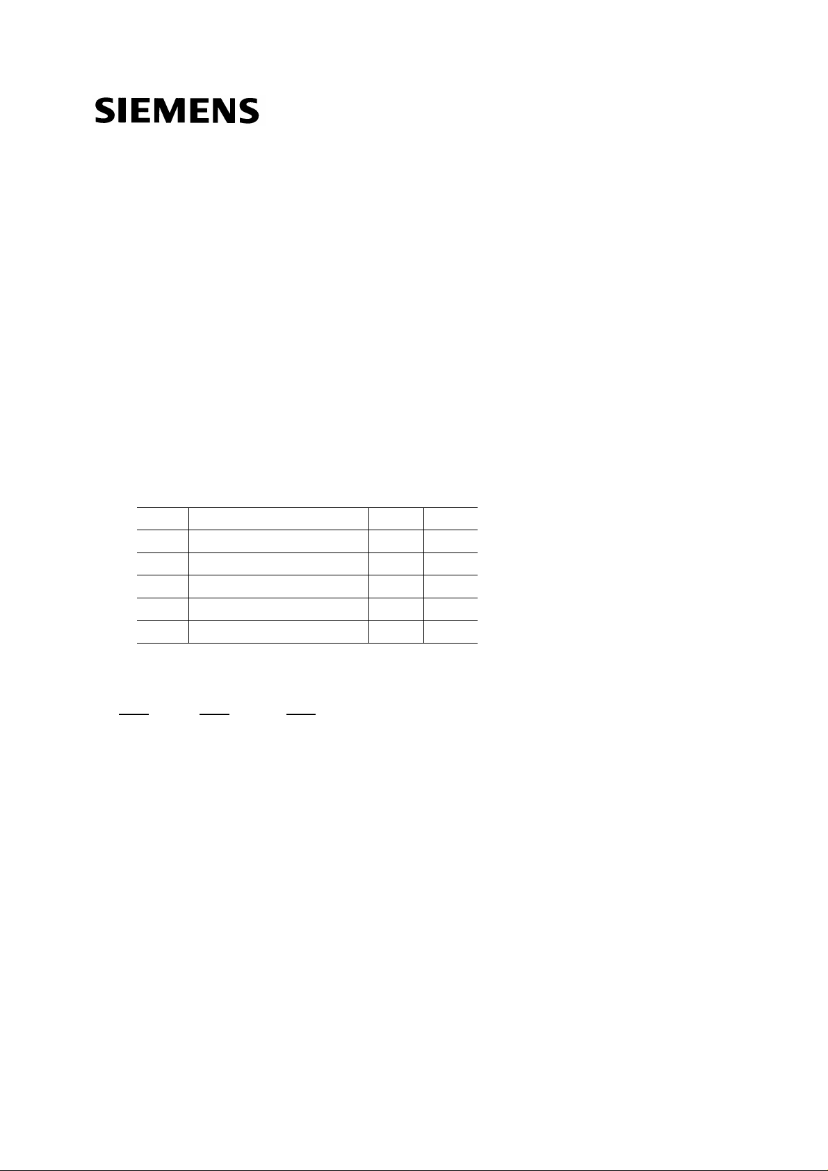
• Performance:
-50 -60
tRAC RAS Access Time 50 ns 60 ns
tCAC CAS Access Time 13 ns 15 ns
tAA Access Time from Address 25 ns 30 ns
tRC Cycle Time 84 ns 104 ns
tHPC EDO Mode Cycle Time 20 ns 2 5 ns
• Single +3.3 V ± 0.3 V Power Supply
• CAS-before-RAS refresh, RAS-only-refresh
• Decoupling capacitors mounted on substrate
• All inputs, outputs and clocks are fully LV-TTL compatible
• Serial presence detects (optional)
• Utilizes 8M × 8 -DRAMs in TSOPII packages
• 4096 refresh cycles / 64 ms with 12 / 11 addressing (Row / Column) for HYM64/72V8005GU
• 8192 refresh cycles / 128 ms with 13 / 10 addressing (Row / Column) for HYM64/72V8045GU
• Gold contact pad
• Card Size: 133,35mm x 25,40 mm x 4,00 mm
• This DRAM product module family is intended to be fully pin and architecture compatible
with the 168pin unbuffered SDRAM DIMM module family
Semiconductor Group 1
1 2.97
HYM 64(72)V8005/45GU-50/-60
8M x 64/72 DRAM Module
The HYM64(72)V2005/45GU-50/-60 are industry standard 168-pin 8-byte Dual In-Line Memory
Modules (DIMMs) which are organized as 8M x 64 and 8M x 72 high speed memory arrays
designed with EDO DRAMs for non-parity and ECC applications. 4k refresh with 12 / 11 addressing
and 8k refresh modules with 13 / 10 addressing are available.The DIMMs use eight 8M x 8 EDO
DRAMs for the 8M x 64 organisation and nine 8M x 8 DRAMs for the 8M x 72 organisation, both in
TSOPII packages. Decoupling capacitors are mounted on the PC board.
The DIMMs use optional serial presence detects implemented via a serial E
2
C protocol. The first 128 bytes are utilized by the DIMM manufacturer and the second 128
pin I
bytes of serial PD data are available to the customer.
All 168-pin DIMMs provide a high performance, flexible 8-byte interface in a 133,35 mm long spacesaving footprint.
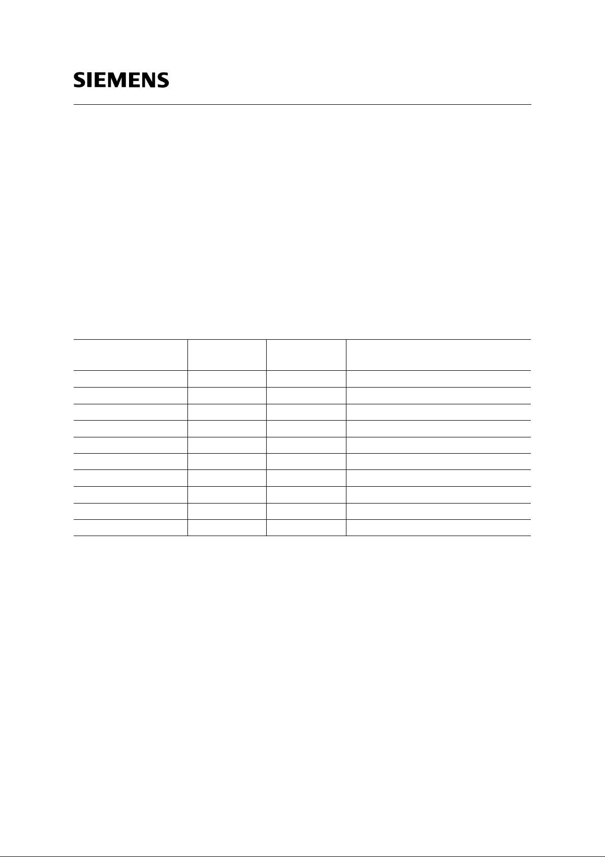
Ordering Information
2
PROM using the two
Type Ordering
Package Descriptions
Code
4k-Refresh:
HYM 64V8005GU-50 Q67100-Q2188 L-DIM-168-13 8M x 64 DRAM module (access time 50 ns)
HYM 64V8005GU-60 Q67100-Q2189 L-DIM-168-13 8M x 64 DRAM module (access time 60 ns)
HYM 72V8005GU-50 L-DIM-168-13 8M x 72 DRAM module (access time 50 ns)
HYM 72V8005GU-60 L-DIM-168-13 8M x 72 DRAM module (access time 60 ns)
8k-Refresh:
HYM 64V8045GU-50 L-DIM-168-13 8M x 64 DRAM module (access time 50 ns)
HYM 64V8045GU-60 L-DIM-168-13 8M x 64 DRAM module (access time 60 ns)
HYM 72V8045GU-50 L-DIM-168-13 8M x 72 DRAM module (access time 50 ns)
HYM 72V8045GU-60 L-DIM-168-13 8M x 72 DRAM module (access time 60 ns)
Semiconductor Group 2
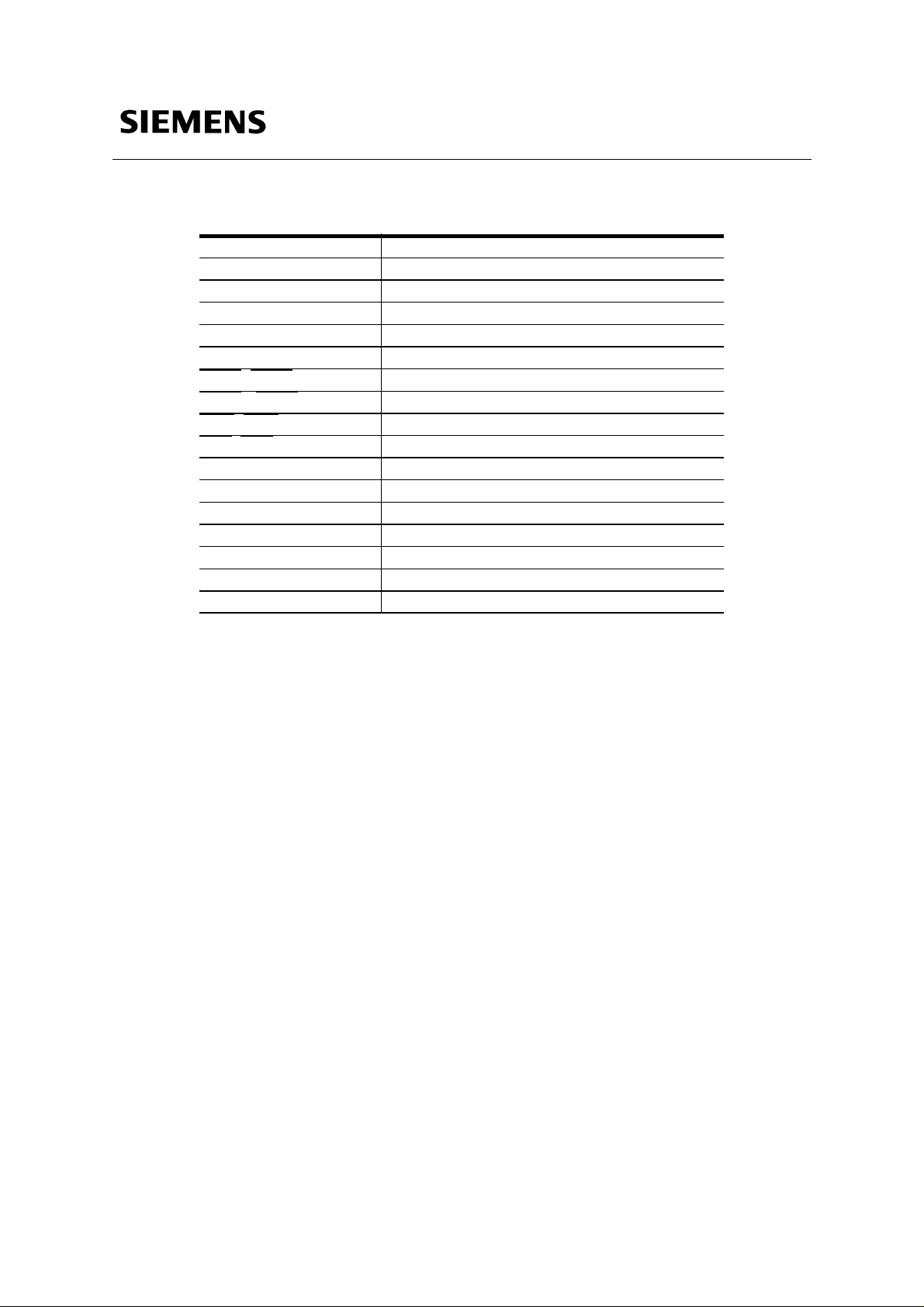
Pin Names
A0-A11 Row Address Input for HYM64/72V8005
A0-A10 Column Address Input for HYM64/72V8005
A0-A12 Row Address Input for HYM64/72V8045
A0-A9 Column Address Input for HYM64/72V8045
DQ0 - DQ63 Data Input/Output
CB0-CB7 Check Bit Data Input/Output ( x72 only)
RAS0
CAS0
WE0
OE0
Vcc Power (+3.3 Volt)
Vss Ground
SCL Clock for Presence Detect
SDA Serial Data Out for Presence Detect
SA0-SA2 Serial Presence Detect Addresses
N.C. No Connection
DU Don’t use
HYM 64(72)V8005/45GU-50/-60
, RAS2 Row Address Strobe
- CAS7 Column Address Strobe
, WE2 Read / Write Input
, OE2 Output Enable
8M x 64/72 DRAM Module
Semiconductor Group 3
HYM 64(72)V8005/45GU-50/-60
8M x 64/72 DRAM Module
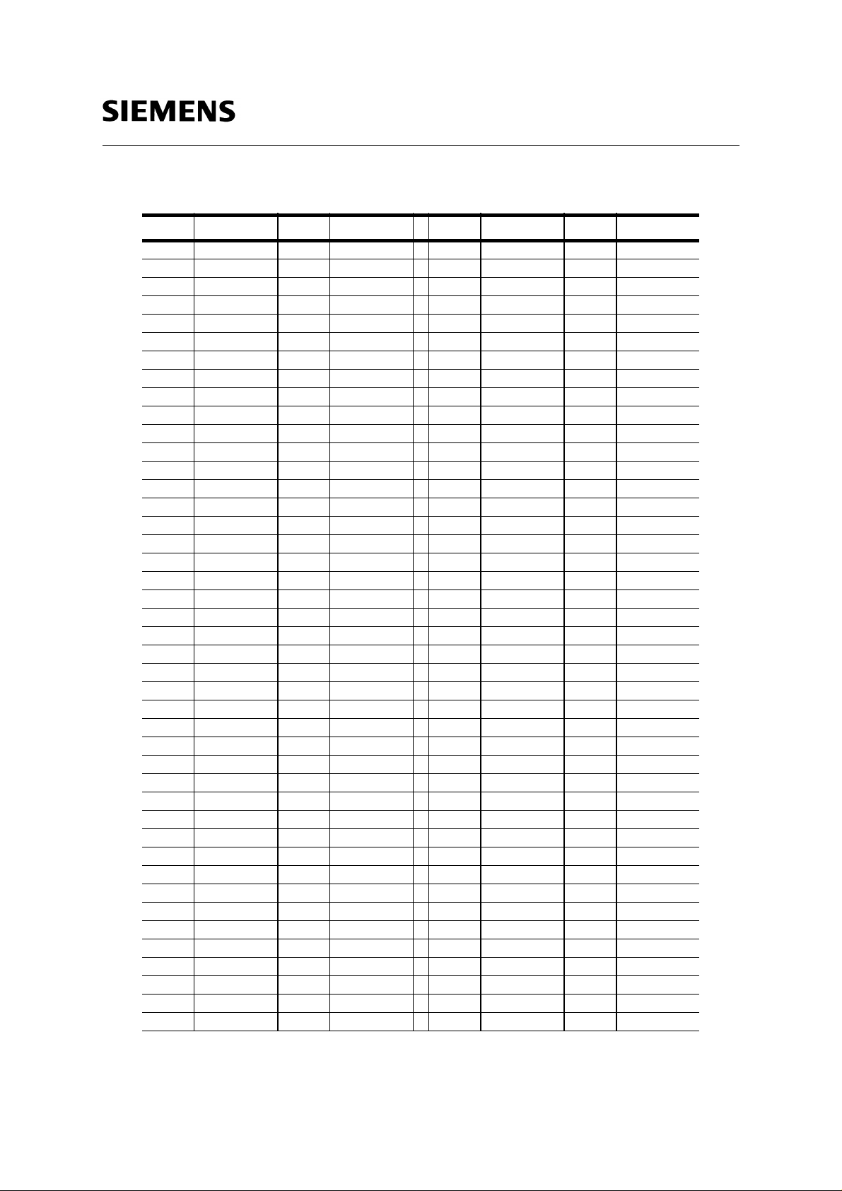
Pin Configuration
PIN # Symbol PIN # Symbol PIN # Symbol PIN # Symbol
1 VSS 43 VSS 85 VSS 127 VSS
2 DQ0 44 OE2 86 DQ32 128 DU
3 DQ1 45 RAS2 87 DQ33 129 NC
4 DQ2 46 CAS2 88 DQ34 130 CAS6
5 DQ3 47 CAS3 89 DQ35 131 CAS7
6 VCC 48 WE2 90 VCC 132 DU
7 DQ4 49 VCC 91 DQ36 133 VCC
8 DQ5 50 NC 92 DQ37 134 NC
9 DQ6 51 NC 93 DQ38 135 NC
10 DQ7 52 CB3 94 DQ39 136 CB6
11 DQ8 53 CB3 95 DQ40 137 CB7
12 VSS 54 VSS 96 VSS 138 VSS
13 DQ9 55 DQ16 97 DQ41 139 DQ48
14 DQ10 56 DQ17 98 DQ42 140 DQ49
15 DQ11 57 DQ18 99 DQ43 141 DQ50
16 DQ12 58 DQ19 100 DQ44 142 DQ51
17 DQ13 59 VCC 101 DQ45 143 VCC
18 VCC 60 DQ20 102 VCC 144 DQ52
19 DQ14 61 NC 103 DQ46 145 NC
20 DQ15 62 DU 104 DQ47 146 DU
21 CB0 63 NC 105 CB4 147 NC
22 CB1 64 VSS 106 CB5 148 VSS
23 VSS 65 DQ21 107 VSS 149 DQ53
24 NC 66 DQ22 108 NC 150 DQ54
25 NC 67 DQ23 109 NC 151 DQ55
26 VCC 68 VSS 110 VCC 152 VSS
27 WE0 69 DQ24 111 DU 153 DQ56
28 CAS0 70 DQ25 112 CAS4 154 DQ57
29 CAS1 71 DQ26 113 CAS5 155 DQ58
30 RAS0 72 DQ27 114 NC 15 6 DQ59
31 OE0 73 VCC 115 DU 157 VCC
32 VSS 74 DQ28 116 VSS 158 DQ60
33 A0 75 DQ29 117 A1 159 DQ61
34 A2 76 DQ30 118 A3 160 DQ62
35 A4 77 DQ31 119 A5 161 DQ63
36 A6 78 VSS 120 A7 162 VSS
37 A8 79 NC 121 A9 163 NC
38 A10 80 NC 122 A11 164 NC
39 A12 81 NC 123 NC 165 SA0
40 VCC 82 SDA 124 VCC 166 SA1
41 VCC 83 SCL 125 DU 167 SA2
42 DU 84 VCC 126 DU 168 VCC
Semiconductor Group 4
HYM 64(72)V8005/45GU-50/-60
8M x 64/72 DRAM Module
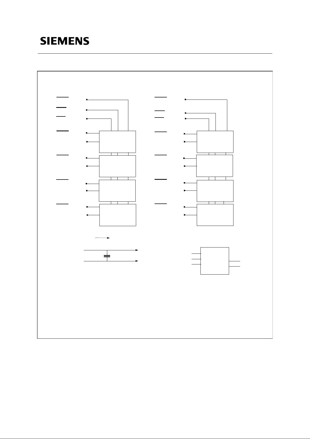
RAS0
WE0
OE0
CAS0
DQ0-DQ7
CAS1
DQ8-DQ15
CAS2
DQ16-DQ23
CAS3
DQ24-DQ31
A0-A11,(A12)
VCC
VSS
I/O1-I/O8
I/O1-I/O8
I/O1-I/O8
I/O1-I/O8
D0-D7
C0-C7
D0
D1
D2
D3
RAS2
WE2
OE2
CAS4
DQ32-DQ39
CAS5
DQ40-DQ47
CAS6
DQ48-DQ55
CAS7
DQ56-DQ63
I/O1-I/O8
D4
I/O1-I/O8
D5
I/O1-I/O8
D6
I/O1-I/O8
D7
E2PROM (256wordx8bit)
SA0
SA1
SCL
SA2
SDA
8M x 64 DIMM Module Block Diagram
Semiconductor Group 5
HYM 64(72)V8005/45GU-50/-60
8M x 64/72 DRAM Module
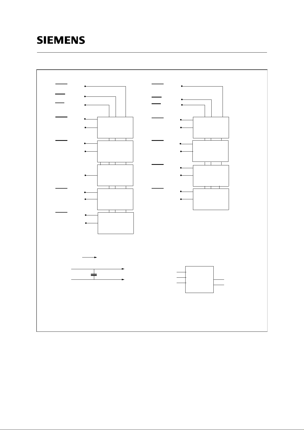
RAS0
WE0
OE0
CAS0
DQ0-DQ7
CAS1
DQ8-DQ15
CB0-CB7
CAS2
DQ16-DQ23
CAS3
DQ24-DQ31
I/O1-I/O8
I/O1-I/O8
I/O1-I/O8
I/O1-I/O8
I/O1-I/O8
D0
D1
D8
D2
D3
RAS2
WE2
OE2
CAS4
DQ32-DQ39
CAS5
DQ40-DQ47
CAS6
DQ48-DQ55
CAS7
DQ56-DQ63
I/O1-I/O8
D4
I/O1-I/O8
D5
I/O1-I/O8
D6
I/O1-I/O8
D7
A0-A11,(A12)
VCC
VSS
D0-D7
C0-C8
8M x 72 DIMM Module Block Diagram
Semiconductor Group 6
E2PROM (256wordx8bit)
SA0
SA1
SCL
SA2
SDA

TRUTH TABLE
HYM 64(72)V8005/45GU-50/-60
8M x 64/72 DRAM Module
FUNCTION RAS CAS WRITE OE ROW
ADDR
Standby H X X X X X High Impedance
Read L L H L ROW COL Data Out
Early-Write L L L X ROW COL Data In
Late-Write L L H - L H ROW COL Data In
Read-Modify-Write
(RMW)
EDO Page Mode Read 1st Cycle L H - L H L ROW COL Data Out
2nd Cycle L H - L H L n/a COL Data Out
EDO Page Mode Write 1st Cycle L H - L L X ROW COL Data In
2nd Cycle L H - L L X n/a COL Data In
EDO Page Mode RMW 1st Cycle L H - L H - L L - H ROW COL Data Out, Data In
2st Cycle L H - L H - L L - H n/a COL Data Out, Data In
RAS only refresh L H X X ROW n/a High Impedance
CAS-before-RAS refresh H - L L H X X n/a High Impedance
Hidden Refresh READ L-H-L L H L ROW COL Data Out
WRITE L-H-L L L X ROW COL Data In
Self Refresh H - L L H X X X High Impedance
L L H - L L - H ROW COL Data Out, Data In
COL
ADDR
DQ0-DQ63
Semiconductor Group 7

HYM 64(72)V8005/45GU-50/-60
8M x 64/72 DRAM Module
Absolute Maximum Ratings
Operating temperature range ......................................................................................... 0 to + 70 °C
Storage temperature range...................................................................................... – 55 to + 125 °C
Input/output voltage .............................................................................. –0.5 to min (Vcc+0.5, 4.6) V
Power supply voltage.................................................................................................... –0.5 to 4.6 V
Power dissipation.................................................................................................................. 4.97 W
Data out current (short circuit) ................................................................................................ 50 mA
Stresses above those listed under "Absolute Maximum Ratings" may cause permanent
Note:
damage to the device. Exposure to absolute maximum rating conditions for extended periods
may affect device reliability.
DC Characteristics
T
= 0 to 70 °C;
A
V
= 3.3 V ± 0.3 V
CC
Parameter Symbol x 64/ x72 Unit Notes
min. max.
Input high voltage
Input low voltage
Output high voltage (LVTTL)
I
Output „H“ level voltage (
= – 2 mA)
OUT
Output low voltage (LVTTL)
I
Output „L“ level voltage (
= + 2 mA)
OUT
Output high voltage (LVCMOS)
I
Output „H“ level voltage (
=– 100µA)
OUT
Output low voltage (LVCMOS)
I
Output „L“ level voltage (
=+100 µA)
OUT
Input leakage current
V
(0 V <
< Vcc, all other pins = 0 V)
IN
Output leakage current
V
(DO is disabled, 0 V <
OUT
< Vcc)
V
V
V
V
V
V
I
I
I(L)
O(L)
IH
IL
OH
OL
OH
OL
2.0 Vcc + 0.5 V 1)
– 0.5 0.8 V 1)
2.4 – V 1)
– 0.4 V 1)
Vcc-0.2 – V 1)
– 0.4 V 1)
– 10 10 µA1)
– 10 +10 µA1)
Semiconductor Group 8

HYM 64(72)V8005/45GU-50/-60
8M x 64/72 DRAM Module
DC Characteristics for HYM64/72V8005
T
= 0 to 70 °C;
A
Parameter Symbol x 64 x 72 Unit Note
Average
V
V
= 3.3 V ± 0.3 V
CC
supply current:
CC
-50 version
-60 version
I
CC1
min. max. min. max.
–
–
1120
960
s
–
–
1260
1080mAmA
2) 3)
4)
(RAS, CAS, address cycling,
Standby
(RAS = CAS =
Average
V
supply current
CC
V
one address change)
IH,
V
supply current during RAS
CC
t
RC
only refresh cycles:
-50 version
-60 version
cycling, CAS =
(RAS
Average
V
supply current during
CC
VIH, t
RC
=
hyper page mode (EDO):
-50 version
-60 version
=
V
(RAS
t
=
PC
Standby
(RAS = CAS =
CAS, address cycling
IL,
t
min.)
PC
V
supply current
CC
V
– 0.2 V, one address
CC
change)
V
Average
supply current during
CC
CAS-before-RAS refresh mode:
-50 version
-60 version
=
t
t
RC
RC
min.)
min.)
I
I
I
I
I
CC2
CC3
CC4
CC5
CC6
–8–9mA–
2) 4)
–
–
–
–
1120
960
840
640
–
–
–
–
1260
1080mAmA
945
720mAmA
2) 3)
4)
–4–4,5mA–
–
–
1120
920
–
–
1280
1035mAmA
2) 4)
, CAS cycling
(RAS
, t
RC
=
t
RC
min.)
Semiconductor Group 9

HYM 64(72)V8005/45GU-50/-60
8M x 64/72 DRAM Module
DC Characteristics for HYM64/72V8045
T
= 0 to 70 °C;
A
Parameter Symbol x 64 x 72 Unit Note
V
= 3.3 V ± 0.3 V
CC
min. max. min. max.
s
Average
(RAS, CAS, address cycling,
Standby
(RAS = CAS =
Average
V
supply current:
CC
V
supply current
CC
V
one address change)
IH,
V
supply current during RAS
CC
only refresh cycles:
cycling, CAS =
(RAS
Average
V
supply current during
CC
VIH, t
hyper page mode (EDO):
=
V
(RAS
t
=
PC
Standby
(RAS = CAS =
CAS, address cycling
IL,
t
min.)
PC
V
supply current
CC
V
– 0.2 V, one address
CC
change)
-50 version
-60 version
t
=
t
RC
RC
-50 version
-60 version
=
t
RC
min.)
RC
-50 version
-60 version
min.)
I
I
I
I
I
CC1
CC2
CC3
CC4
CC5
–
–
800
720
–
–
900
810mAmA
2) 3)
4)
–8–9mA–
2) 4)
–
–
–
–
800
720
840
640
–
–
–
–
900
810mAmA
945
720mAmA
2) 3)
4)
–4–4,5mA–
Average
supply current during
CC
I
CC6
V
CAS-before-RAS refresh mode:
-50 version
-60 version
, CAS cycling
(RAS
, t
RC
=
t
RC
min.)
Semiconductor Group 10
–
–
1120
920
–
12601
–
035mAmA
2) 4)

HYM 64(72)V8005/45GU-50/-60
8M x 64/72 DRAM Module
AC Characteristics
T
= 0 to 70 °C,VCC = 3.3 V ± 0.3 V, tT = 2 ns
A
5)6)
Parameter
common parameters
Random read or write cycle time t
precharge time t
RAS
pulse width t
RAS
pulse width t
CAS
Row address setup time t
Row address hold time t
Column address setup time t
Column address hold time t
to CAS delay time t
RAS
to column address delay t
RAS
hold time t
RAS
hold time t
CAS
to RAS precharge time t
CAS
Transition time (rise and fall) t
Refresh period for 4k-refresh t
Refresh period for 8k-refresh t
Symbol
RC
RP
RAS
CAS
ASR
RAH
ASC
CAH
RCD
RAD
RSH
CSH
CRP
T
REF
REF
Limit Values
Unit Note
-50 -60
min. max. min. max.
84 – 104 – ns
30 – 40 – ns
50 10k 60 10k ns
8 10k 10 10k ns
0–0–ns
8–10–ns
0–0–ns
8–10–ns
12 37 14 45 ns
10 25 12 30 ns
13 15 – ns
40 50 – ns
5–5–ns
1 50 1 50 ns 7
–64–64ms
– 128 – 128 ms
16E
Read Cycle
Access time from RAS t
Access time from CAS
Access time from column address t
access time t
OE
Column address to RAS
lead time t
Read command setup time t
Read command hold time t
Read command hold time referenced to
t
t
RAC
CAC
AA
OEA
RAL
RCS
RCH
RRH
RAS
to output in low-Z t
CAS
Output buffer turn-off delay t
CLZ
OFF
Semiconductor Group 11
– 50 – 60 ns 8, 9
– 13 – 15 ns 8, 9
– 25 – 30 ns 8,10
–13–15ns
25 – 30 – ns
0–0–ns
0–0–ns11
0–0–ns11
0–0–ns8
0 13 0 15 ns 12

HYM 64(72)V8005/45GU-50/-60
8M x 64/72 DRAM Module
AC Characteristics (cont’d)
T
= 0 to 70 °C,VCC = 3.3 V ± 0.3 V, tT = 2 ns
A
5)6)
Parameter
Output turn-off delay from OE t
Data to CAS
Data to OE
high to data delay t
CAS
high to data delay t
OE
low delay t
low delay t
Write Cycle
Write command hold time t
Write command pulse width t
Write command setup time t
Write command to RAS
Write command to CAS
lead time t
lead time t
Data setup time t
Data hold time t
Symbol
OEZ
DZC
DZO
CDD
ODD
WCH
WP
WCS
RWL
CWL
DS
DH
Limit Values
Unit Note
-50 -60
min. max. min. max.
0 13 0 15 ns 12
0–0–ns13
0–0–ns13
10 – 13 – ns 14
10 – 13 – ns 14
8–10–ns
8–10–ns
0–0–ns15
13 – 15 – ns
13 – 15 – ns
0–0–ns16
8–10–ns16
16E
Read-modify-Write Cycle
Read-write cycle time t
to WE delay time t
RAS
to WE delay time t
CAS
Column address to WE
command hold time t
OE
delay time t
RWC
RWD
CWD
AWD
OEH
Hyper Page Mode (EDO) Cycle
EDO cycle time t
precharge time t
CAS
Access time from CAS
precharge t
Output data hold time t
pulse width in EDO mode t
RAS
precharge to RAS Delay t
CAS
setup time prior to CAS t
OE
HPC
CP
CPA
COH
RAS
RHPC
OES
Semiconductor Group 12
113 – 138 – ns
64 – 77 – ns 15
27 – 32 – ns 15
39 – 47 – ns 15
10 – 13 – ns
20 – 25 – ns
8–10–ns
– 27 – 32 ns 7
5–5–ns
50 200k 60 200k ns
27 – 32 – ns
5–5–ns

HYM 64(72)V8005/45GU-50/-60
8M x 64/72 DRAM Module
AC Characteristics (cont’d)
T
= 0 to 70 °C,VCC = 3.3 V ± 0.3 V, tT = 2 ns
A
Parameter
5)6)
Symbol
min. max. min. max.
Hyper Page Mode (EDO) Read-modify-Write Cycle
Hyper page mode (EDO) read-write
t
PRWC
58 – 68 – ns
cycle time
precharge to WE t
CAS
CPWD
41 – 49 – ns
CAS-before-RAS Refresh Cycle
CAS setup time t
hold time t
CAS
to CAS precharge time t
RAS
Write to RAS
precharge time t
Write hold time referenced to RAS
CSR
CHR
RPC
WRP
t
WRH
10 – 10 – ns
10 – 10 – ns
5–5–ns
10 – 10 – ns
10 – 10 – ns
Limit Values
-50 -60
16E
Unit Note
Capacitance
T
= 0 to 70 °C;
A
V
= 3.3 V ± 0.3 V; f = 1 MHz
CC
Parameter Symbol Limit Values Unit
min. max.
Input Capacitance (A0 to A11,(A12))
Input Capacitance (RAS
Input Capacitance (CAS0
Input Capacitance (WE0
0, RAS2)
-CAS7)
,WE2,OE0,OE2)
I/O Capacitance (DQ0-DQ63,CB0-CB8)
Input Capacitance (SCL, SA0-2) C
C
C
C
C
C
I1
I2
I3
I4
IO1
s
–55pF
–50pF
–10pF
–50pF
–11pF
–8pF
Input/Output Capacitance (SDA) Cs – 10 pF
Semiconductor Group 13

HYM 64(72)V8005/45GU-50/-60
8M x 64/72 DRAM Module
Notes:
1) All voltages are referenced to VSS.
I
, I
, I
2)
CC1
CC3
I
and I
3)
CC1
and I
CC4
depend on output loading. Specified values are obtained with the output open.
CC4
4) Address can be changed once or less while RAS = Vil. In case of ICC4 it can be changed once or less during
a hyper page mode (EDO) cycle
5) An initial pause of 200 µs is required after power-up followed by 8 RAS cycles of which at least one cycle has
to be a refresh cycle, before proper device operation is achieved. In case of using the internal refresh counter,
a minimum of 8 CAS-before-RAS
6) AC measurements assume
V
7)
IH
(min.)
and V
measured between
8) Measured with the specified current load and 100 pF at Vol = 0.8 V and Voh = 2.0 V. Access time is determined
by the latter of t
depend on cycle rate.
CC6
initialization cycles instead of 8 RAS cycles are required.
t
= 2 ns.
T
are reference levels for measuring timing of input signals. Transition times are also
IL (max.)
V
and VIL.
IH
, t
RAC
CAC
, tAA,t
CPA ,tOEA
. t
is measured from tristate.
CAC
9) Operation within the t
only. If t
is greater than the specified t
RCD
10) Operation within the t
only. If t
11) Either t
12) t
OFF (max.)
is greater than the specified t
RAD
or t
RCH
, t
must be satisfied for a read cycle.
RRH
OEZ (max.)
define the time at which the output achieves the open-circuit conditions and are not
referenced to output voltage levels. t
limit ensures that t
RCD (max.)
limit ensures that t
RAD (max.
)
can be met. t
RAC (max.)
RCD (max.)
RAD (max.)
is referenced from the rising edge of RAS or CAS, whichever occurs
OFF
limit, then access time is controlled by t
can be met. t
RAC (max.)
limit, then access time is controlled by tAA.
RCD (max.)
RAD (max.)
is specified as a reference point
.
CAC
is specified as a reference point
last.
13) Either
14) Either
15) t
t
or t
DZC
t
CDD
, t
RWD
, t
WCS
electrical characteristics only. If t
must be satisfied.
DZO
or t
must be satisfied.
ODD
and t
CWD
are not restrictive operating parameters. They are included in the data sheet as
AWD
WCS
> t
, the cycle is an early write cycle and data out pin will remain
WCS (min.)
open-circuit (high impedance) through the entire cycle; if t
RWD
> t
RWD (min.)
, t
CWD
> t
CWD (min.)
and t
AWD
> t
the cycle is a read-write cycle and I/O will contain data read from the selected cells. If neither of the above
sets of conditions is satisfied, the condition of I/O (at access time) is indeterminate.
16) These parameters are referenced to the CAS
leading edge in early write cycles and to the WE leading edge
in read-write cycles.
AWD (min.)
,
Semiconductor Group 14

HYM 64(72)V8005/45GU-50/-60
8M x 64/72 DRAM Module
Serial Presence Detects:
A serial presence detect storage device -- EEPROM 24C02 -- is assembled on to the module.
Information about the modul confuguration, speed, etc. is written into the EEPROM device during
module production using a serial presence detect protocol ( I
2
C synchronous 2-wire bus).
64
V8005
GU-60
Hex
HYM
72
V8005
GU-50
72
V8005
GU-60
Byte#
Description
SPD Entry Value
0 Number of SPD bytes 128 80 80 80 80
1 Total bytes in Serial PD 256 08 08 08 08
2 Memory Type EDO 02 02 02 02
3 Number of Row Addresses 12 0C 0C 0C 0C
4 Number of Column Addresses 11 0B 0B 0B 0B
5 Number of DIMM Banks 1 01 01 01 01
6 Module Data Width x64 / x72 40 40 48 48
7 Module Data Width (cont’d) 0 00000000
8 Module Interface Levels LVTTL 01 01 01 01
9 RAS access time 50 / 600 ns 32 3C 32 3C
10 CAS access time 13 / 15 ns 0D 0F 0D 0F
11 Dimm Config (Error Det/Corr.) none / ECC 00 00 02 02
12 Refresh Rate/Type normal
15.6µs
13 Primary DRAM data width x8 08 08 08 08
14 Error checking DRAM data width none / x8 00 00 08 08
15-31 reserved for future offerings FF FF FF FF
32 Superset Memory Type NA FF FF FF FF
33-61 Superset information (may be used in
future)
62 SPD Revision Designator Rev. 1.0 01 01 01 01
63 Checksum for bytes 0-62 XX XX XX XX
64-127 Manufacturer Information (optional) FF FF FF FF
128-
Unused Storage Locations FF FF FF FF
255
NA FF FF FF FF
64
V8005
GU-50
00 00 00 00
Semiconductor Group 15

Serial Presence Detects (cont’d):
HYM 64(72)V8005/45GU-50/-60
8M x 64/72 DRAM Module
64
V4045
GU-60
Hex
HYM
72
V4045
GU-50
72
V4045
GU-60
Byte#
Description
SPD Entry Value
0 Number of SPD bytes 128 80 80 80 80
1 Total bytes in Serial PD 256 08 08 08 08
2 Memory Type EDO 02 02 02 02
3 Number of Row Addresses 13 0D 0D 0D 0D
4 Number of Column Addresses 10 0A 0A 0A 0A
5 Number of DIMM Banks 1 01 01 01 01
6 Module Data Width x64 / x72 40 40 48 48
7 Module Data Width (cont’d) 0 00000000
8 Module Interface Levels LVTTL 01 01 01 01
9 RAS access time 50 / 60 ns 32 3C 32 3C
10 CAS access time 13 / 15 ns 0D 0F 0D 0F
11 Dimm Config (Error Det/Corr.) none / ECC 00 00 02 02
12 Refresh Rate/Type normal
15.6µs
13 Primary DRAM data width x8 08 08 08 08
14 Error checking DRAM data width none / x8 00 00 08 08
15-31 reserved for future offerings FF FF FF FF
32 Superset Memory Type NA FF FF FF FF
33-61 Superset information (may be used in
future)
62 SPD Revision Designator Rev. 1.0 01 01 01 01
63 Checksum for bytes 0-62 XX XX XX XX
64-127 Manufacturer Information (optional) FF FF FF FF
128-
Unused Storage Locations FF FF FF FF
255
NA FF FF FF FF
64
V4045
GU-50
00 00 00 00
Semiconductor Group 16

HYM 64(72)V8005/45GU-50/-60
L-DIM-168-13
Module package
(168 pin, dual read-out, single in-line memory module)
133,35
1
3,0
10 11 40 41
A
85
94 95
127,35
BC
124 125
84
168
* )
25,40
17,78
8M x 64/72 DRAM Module
3,125
6,35
Detail A
2,0
3,125
6,35
Detail B
*) 4.00 max for modules assembled with TSOPII-packages
9.00 max for modules assembled with SOJ-packages
1,27
2,54 min.
2,0
Detail C
preliminary drawing
1,0 + 0.5
-
+
0,2 0,15
-
DM168-13.WMF
Semiconductor Group 17
 Loading...