

Page 1
400 Hot Springs Road, Carson City NV 89706 • (775) 883-0820 • Fax (775) 883-0827 • www.hytek.com • 25
High Speed Laser Diode Driver
driver. The laser diode can be driven through a transmission
line without the need for a matched impedance termination.
This removes a large source of heat that can be detrimental
to high performance laser diode systems.
The HY6510 is used in applications that require digital, high speed current modulation of the laser diode. The
HY6510 input is ECL compatible and is terminated into
50Ω. The HY6510 uses a GaAsFET current switch that
drives a laser diode with modulation currents of up to
400mA peak-to-peak. Two programmable current sources
allow user selectability of the bias and modulation currents.
The pre-bias current is selectable from zero to 40mA. The
Modulation current is selectable from zero to 400mA. These
selected currents modulate the laser beam at the input frequency . The HY6510 comes in a 32 pin dual in-line ceramic
package. This package provides a cost effective alternative
to the hermetic package of the HY6410 driver. An aluminum
heat spreader is included as part of the package for heat
sinking the device.
HY6510
Laser Diode Driver
Features:
✦ Single ended ECL input (50Ω)
✦ Data rates up to 622Mbps
✦ Programmable bias current
✦ Adjustable modulation current
✦ Patented “backmatching” thermal manage-
ment
✦ Backmatched output allows remote drive
through 50Ω line
✦ Thru-hole or surface-mount packaging
TEC Controllers Laser Diode Drivers Micro-heaters
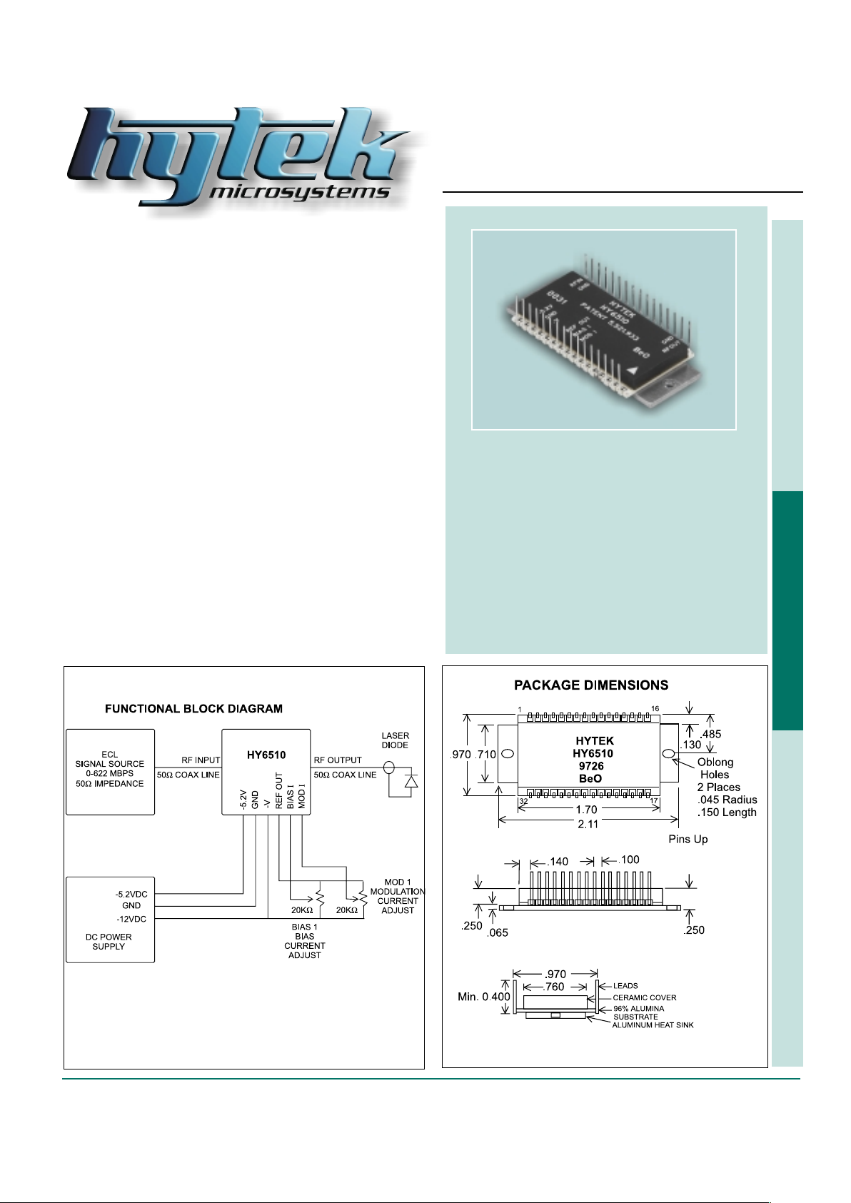
Figure 1
Figure 2
Page 2
26 • 400 Hot Springs Road, Carson City NV 89706 • (775) 883-0820 • Fax (775) 883-0827 • www.hytek.com
HY6510
Laser Diode Driver
Pin Descriptions
> –5.2V INPUT: Power supply input for ECL buffer circuitry .
> GROUND: Ground return for –5.2V ECL supply and –V .
> –V: Power Supply input for Bias and Modulation currents as well as laser diode drive circuitry .
> REF OUT : Precision reference output, +5V with respect to –V (if –V is –12V , REF OUT would be –7V).
> BIAS I: Input used to set the Bias current for the laser diode. Maximum bias current occurs when the voltage at
the BIAS I input is +2V with respect to the –V input. The voltage at the BIAS I input for a given bias current is determined by the equation: V(BIAS I) = –V + (desired bias current) x 40
ΩΩ
ΩΩ
Ω
> MOD I: Input used to set the Modulation current for the laser diode. This current is added to the Bias I current
which always flows through the laser diode. Maximum modulation current occurs when the voltage at the
MOD I input is +0.5V with respect to the –V input. The current set by the MOD I voltage is controlled by
the ECL RF input. When the RF input is open or set to an ECL “low” input, only BIAS I current flows
through the laser diode. The voltage at the MOD I input for a given modulation current is determined by
the equation: V(MOD I) = –V + (desired modulation current) x 2.5
ΩΩ
ΩΩ
Ω
> RF IN: The input is terminated with an equivalent 50Ω into –2V required by the ECL logic family . This input ac-
cepts data rates up to 622Mbps.
> RF OUT : The patented “backmatching” technique does not require a 50Ω termination at the laser diode end of the
transmission line.
Input Specifications
Power Inputs
–5.2V Supply –4.9V to –5.5V @ 1 15mA max.
–12V Supply (–V) –9V to –12V @ 420mA max.
RF IN ECL logic levels, 0–600Mbps
BIAS I 0 to 40mA for input voltage –V to –V + 2V
MOD I 0 to 400mA for input voltage –V to –V + 1.0V
Output Specifications
RF OUT Current output into 50Ω transmission line
Low Current = BIAS I, High Current = MOD I
RF OUT Transmission Line Length 10 feet max.
REF OUT –V +5V
Environmental Conditions
Operating T emperature –55°C to 100°C (case)
Storage T emperature –65° to 150°C
Pin Designations
Description HY6510
–5.2V input (–5.2V) Pin 14
Ground (GND) Pins 13, 19, 31
–V Input (–V) Pin 12
Reference Voltage Output (REF OUT) Pin 10
Bias I Adjust (BIAS I) Pin 9
Modulation I Adjust (MOD I) Pin 8
ECL Input Waveform (RF IN) Pin 18
Laser Diode Current Driver (RF OUT) Pin 32
Model No. HY6510
Description: 400mA High Speed Laser Diode Driver;
ceramic package
Application: ECL Digital Modulation of Laser Diode
Ordering Information
 Loading...