

Page 1
High Voltage Current Mode PWM
Controller for ISDN Equipment
Ordering Information
+V
IN Feedback Max
Min Max
15V 250V < ± 1% 49% HV9605P HV9605NG HV9605X
Accuracy Duty Cycle
14 Pin 14 Pin
Plastic DIP Narrow Body SOIC
Package Options
Die
HV9605
HV9605
Preliminary
Features
BiCMOS/DMOS technology
Current mode control
49% duty cycle operation
Programmable START/STOP capability
15V to 250V input range internal start-up regulator
6.0µA standby supply current for +VIN <20V
0.9mA operating supply current
5.0V VDD supply operation
30KHz to 300KHz internal oscillator
15KHz to 150KHz converter output frequency
1.0MHz low offset error amplifier
1.20V 2% band gap reference
Output driver optimized for under 10W applications
Low driver output impedance with VDD = 0V
Fast (90nsec) over current shutdown
All pins are ESD protected
General Description
The Supertex HV9605 is a BiCMOS/DMOS single-output,
current mode, pulse width modulator IC designed to meet
the requirements of ETR-060 for ISDN applications. In a 14
pin package, it provides all the necessary functions to implement a single-switch PWM with a minimum of external parts.
Utilizing Supertex’s proprietary BiCMOS/DMOS technology,
it requires less than one tenth of the operating power of
conventional bipolar PWM ICs. Dynamic range for regulation
is also increased to approximately 8 times that of similar
bipolar parts. It operates directly from any DC input voltage
between 15 and 250 VDC. The START and STOP input
voltage thresholds can be programmed within the operating
input voltage range by means of a resistor divider, provided
+V
IN(START)
eliminating the need for external clamping diodes. The clock
frequency is set with a single external resistor.
> +V
. The output stage is push-pull CMOS,
IN(STOP)
Applications
ISDN network terminations
ISDN terminals
ISDN terminal adapters
Feature phones
SLIC circuits
PBX systems
Modems
Distributed power systems
DC/DC converters
11/30/98
Supertex Inc. does not recommend the use of its products in life support applications and will not knowingly sell its products for use in such applications unless it receives an adequate "products liability
indemnification insurance agreement." Supertex does not assume responsibility for use of devices described and limits its liability to the replacement of devices determined to be defective due to
workmanship. No responsibility is assumed for possible omissions or inaccuracies. Circuitry and specifications are subject to change without notice. For complete liability information covering
this and other Supertex products, refer to the Supertex 1998 Databook.
Absolute Maximum Ratings*
+VIN, Input Voltage -0.5V to +250V
Supply Voltage, V
Operating Temperature Range -40°C to +85°C
Storage Temperature Range -65°C to +150°C
Power Dissipation @ 25°C, SOIC 750mW
Power Dissipation @ 25°C, Plastic DIP 1000mW
*All voltages referenced to GND
1
DD
-0.5V to +10V
11/30/98
Page 2
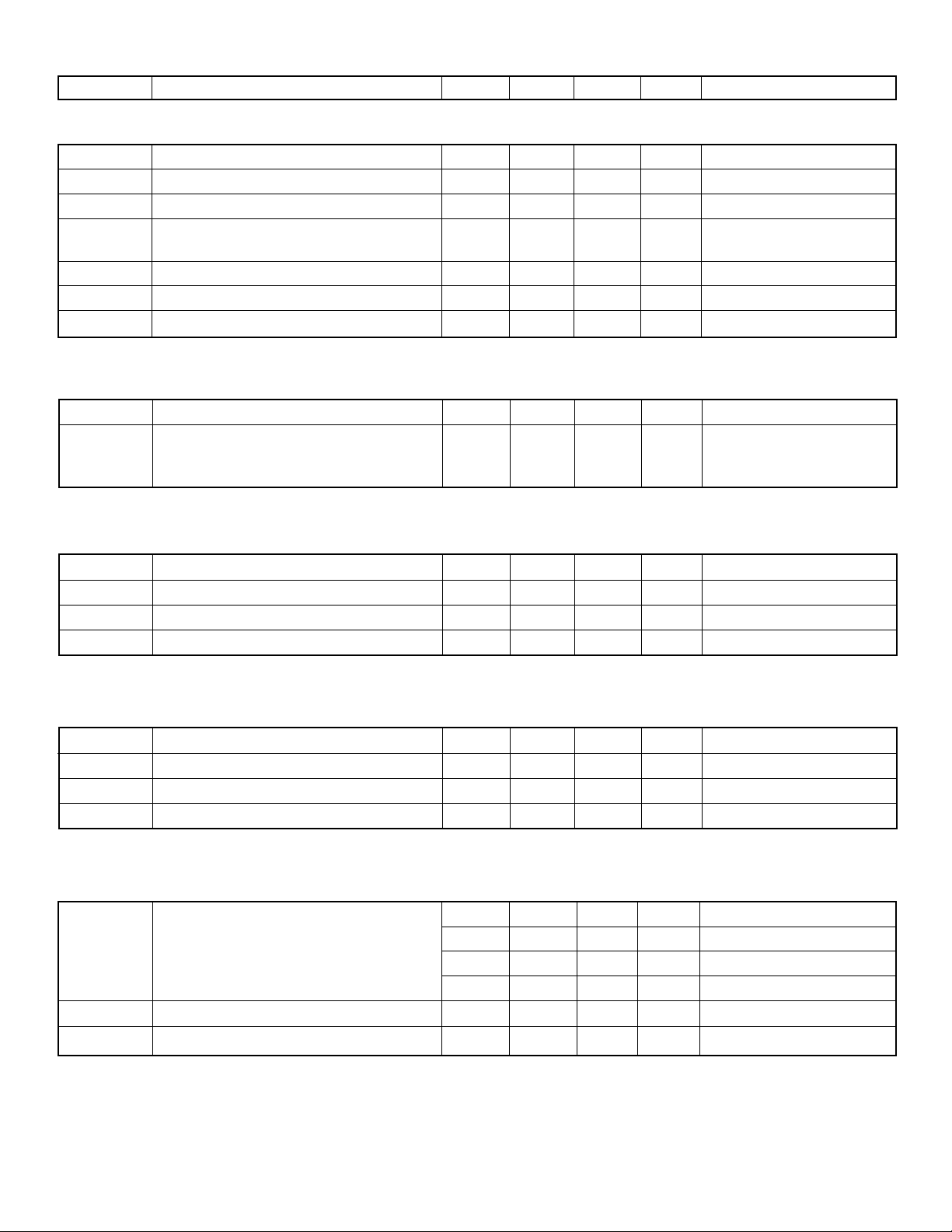
Electrical Characteristics
Symbol Parameters Min Typ Max Unit Conditions
Pre-Regulator/Start-Up
+V
IN
+I
IN
+I
IN
+I
START
V
DD
UVLO Under voltage lockout threshold 4.1 4.2 4.4 V V
HYST Under voltage hysteresis 0.1 0.3 0.4 V
Supply
V
DD
I
DD
Regulator input voltage 15 250 V
Input leakage current 6.0 µA+VIN=20V, Start=0V, Stop=0V
Input leakage current 50 µA+VIN = 250V, VDD = 4.7V
Pre-regulator start-up current 5.0 mA +VIN = 15V,
Start & Stop 10MΩ to + V
Regulator output voltage 4.4 4.5 4.6 V
rising
DD
Operating range 4.7 8.0 V
Supply current 0.9 1.3 mA OUT open,
f
= 20KHz to 150KHz,
OUT
V
= 5V
DD
HV9605
IN
Start/Stop Control
V
START
I
START
I
STOP
V
CLAMP
Start threshold 6.72 7.30 7.88 V
Start input current 0.05 µA+VIN = 18V
Stop input current 0.05 µA+VIN = 18V
Zener clamp voltage on STOP Pin 20 V
MOSFET Driver Output
V
OUT(HIGH)
V
OUT(LOW)
t
R
t
F
Output high voltage 4.85 4.90 V I
Output low voltage 0.05 0.15 V I
Rise time 30 50 nsec CL = 250pf
Fall time 20 50 nsec CL = 250pf
Oscillator
150 KHz RT = 91KΩ
f
OUT
T
C
∆f/f Voltage stability 1 3 % f
Output converter frequency 45 50 55 KHz RT = 390KΩ
31.5 35 38.5 KHz R
18 20 22 KHz R
Temperature coefficient 100 300 PPM/°Cf
= 10mA, VDD = 5.00V
OUT
= -10mA
OUT
= 560KΩ
T
= 1.0MΩ
T
= 50KHz
OUT
= 50KHz, 4.5V< VDD<5.5V
OUT
11/30/98
2
Page 3
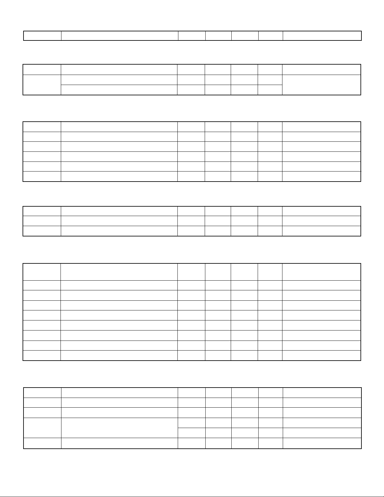
Electrical Characteristics (continued)
Symbol Parameters Min Typ Max Unit Conditions
PWM
D
MAX
D
MIN
Reference
V
REF
V
REF
V
REF
V
REF
I
REF(SHORT)
Maximum duty cycle 49.0 49.9 % f
= 20KHz
OUT
Minimum duty cycle 0 %
Minimum pulse width before pulse drop out 80 125 nsec
Reference output voltage 1.176 1.200 1.224 V TA = 25°C
Load regulation 1.0 5.0 mV 0 < I
REF
Line regulation 2.0 5.0 mV 3.0V < VDD < 5.5V
Reference output voltage 1.159 1.200 1.241 V -40°C < TA < 85°C
Long term stability 3.0 mV T
Short circuit current 0.5 1.0 mA V
= 125°C, 1000hrs
A
= SGND
REF
HV9605
< 0.3mA
Current Sensing
V
CS
V
CS (LIMIT)
t
DELAY
Usable control current sense range VCS (limit) V
Current limit threshold 0.6 0.7 0.8 V
Current limit delay to output 90 120 nsec VCS = 1.5V
Error Amplifier
V
FB
or I
I
FB
NI
V
OS
V
CM
A
VOL
BW Unity gain bandwidth 1.0 1.5 MHz
I
SOURCE
I
SINK
PSRR Power supply rejection 50 72 dB 4.5V < VDD < 5.5V, f=1KHz
Feedback voltage 1.188 1.200 1.212 V REF shorted to NI, FB
shorted to Comp, T
A
Input bias current 25 200 nA VFB = 3.0V, VNI = 2.5V
Input offset voltage 5.0 25 mV
Common mode input range 0 VDD-1 V
Open loop voltage gain 65 90 dB
Output current sourcing -2 -1 mA VFB < V
Output current sinking 2 4 mA VFB > V
NI
NI
= 25°C
Status Output
I
SINK
I
SOURCE
V
STATUS(HIGH)
V
STATUS(LOW)
t
R
Output current sinking 5.0 10 mA V
STATUS
= 2.0V
Output current sourcing 5.0 10 15 µA
High output voltage VDD-0.2 V
DD
V No load
Low output voltage 1.0 2.0 V Sinking 5mA
0.02 0.04 V Sinking 100µA
Rise time 1.0 5.0 msec 4.7nF From Status to GND
11/30/98
3
Page 4

Pin Description
HV9605
SGND - Common connection for all low level signal and digital
circuits. While SGND and PGND must be electrically connected
together, having separate common pins enhances the ability of
the designer to prevent coupling of noise into critical circuits.
PGND - This pin provides common return for the high transient
current of the output driver circuits. While PGND and SGND must
be electrically connected, having a separate connection prevents
common noise created by the high transient currents of the output
driver from being injected into critical circuits.
+V
- This is the start-up linear pre-regulator input which can
IN
accept DC input voltages in the range of 15V to 250V. With
START and STOP set to more than 20V, the leakage current on
this pin is less than 6.0µA at +V
START - The resistive divider from +V
STOP - The resistive divider from +V
V
input voltage to the +V
- This is the supply pin for the PWM circuits. When the
DD
pin exceeds the start voltage the input
IN
= 20V.
IN
sets the start voltage.
IN
sets the stop voltage.
IN
regulator seeks to regulate the voltage on the capacitor connected to this pin to a nominal 4.5V.
OUT - This high current push-pull CMOS output is intended
to drive the gate of a power MOSFET. In order to protect the
power MOSFET in high electrical noise environment, this output
appears as low impedance to PGND when V
is at zero volts.
DD
CS - This is the current sense input to the PWM comparators. Under normal operation the over current limit is triggered
when the voltage on this pin is at 0.70V and the loop control
operating peak current may be set to any level below this, typically
in the range of 0.2 to 0.5V.
COMP - The low impedance output of the error amplifier.
FB - The high impedance inverting input of the error amplifier.
NI - The high impedance non-inverting input of the error
amplifier.
REF - This pin provides a 2% accuracy 1.20V low output
impedance buffered reference which is current limited to 0.5mAmps
and should be bypassed, REF to SGND, with a 0.1µF ceramic
capacitor.
RT - The resistor connected from this pin to SGND sets the
frequency of the internal oscillator by setting the charging current
for the internal timing capacitor. The oscillator frequency is twice
the PWM output frequency.
STATUS - This output is held low until the +V
voltage reaches
IN
the programmed START voltage. It remains low until the bootstrap supply to V
forces the voltage above the internal regulator
DD
set point. It is further held low while the control amplifier output on
the COMP pin is forced to its high limit by a low output from the
converter. Once all these conditions are satisfied, this output will
rise to V
with a time constant set by the external capacitor
DD
indicating that normal operation has been reached. This output
may be used to control the reset of a microprocessor.
Pin Configuration
1
+V
IN
STOP
START
PGND
2
3
4
REF
5
V
DD
6
7
CS
14 Pin SOIC/DIP Package
14
13
12
11
10
9
8
COMP
FB
NI
STATUS
RT
SGND
OUT
11/30/98
4
Page 5
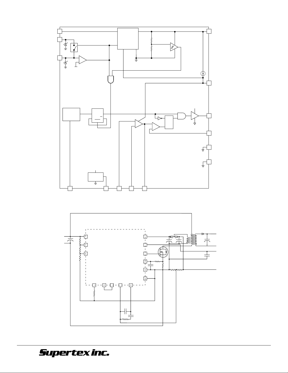
Functional Block Diagram
+V
IN
STOP
START
H=SWITCH CLOSED
L= SWITCH OPEN
+
C
–
V
START
Enable
Start-Up
Regulator
+
–
V
REF
Bootstrap Good
C
UVLO
HV9605
V
DD
Clock
Oscillator
RT
CLK
DQ
CLR
V
DD
Bandgap
Reference
Generator
Q
Typical Application Circuit
+
A
–
REF NI FB COMP
-
+
C
PWM Good
S
Q
R
STATUS
MOSFET Driver
V
DD
OUT
PGND
SGND
CS
48V INPUT
HV9605
+
+
+
-
+V
IN
STOP
START
V
STATUS
OUT
DD
++
TN2124K1
or
TN2524N8
+
ISOLATED
OUTPUT
40V
-
RESET
CS
PGND
SGND
COMPFBNIREFRT
+5.0V
REFERENCED
TO INPUT (-)
TERMINAL
11/30/98
1235 Bordeaux Drive, Sunnyvale, CA 94089
TEL: (408) 744-0100 • FAX: (408) 745-4895
5
www.supertex.com
11/30/98
 Loading...