

Page 1
High Voltage EL Lamp Driver
Ordering Information
Package Options
Device Input Voltage 8-Lead SO Die
HV830 2.0V to 9.5V HV830LG HV830X
HV830
Features
❏ Processed with HVCMOS® technology
❏ 2.0V to 9.5V operating supply voltage
❏ DC to AC conversion
❏ 200V peak-to-peak typical output voltage
❏ Large output load capability – typically 50nF
❏ Permits the use of high-resistance elastomeric lamp
connectors
❏ Adjustable output lamp frequency to control lamp color,
lamp life, and power consumption
❏ Adjustable converter frequency to eliminate harmonics and
optimize power consumption
❏ Enable/disable function
❏ Low current draw under no load condition
❏ Very low standby current – 30nA typical
Applications
❏ Handheld personal computers
❏ Electronic personal organizers
❏ GPS units
❏ Pagers
❏ Cellular phones
❏ Portable instrumentation
General Description
The Supertex HV830 is a high-voltage driver designed for driving
EL lamps of up to 50nF. EL lamps greater than 50nF can be
driven for applications not requiring high brightness. The input
supply voltage range is from 2.0V to 9.5V. The device uses a
single inductor and a minimum number of passive components.
The nominal regulated output voltage that is applied to the EL
lamp is ±100V. The chip can be enabled by connecting the
resistors on R
SW-osc
and R
to VDD and disabled when
EL-osc
connected to GND.
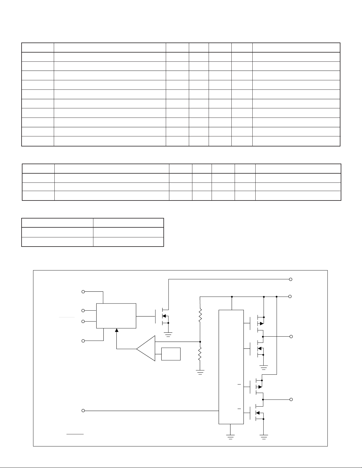
The HV830 has two internal oscillators, a switching MOSFET,
and a high-voltage EL lamp driver. The frequency for the switching converter MOSFET is set by an external resistor connected
between the R
pin and the supply pin VDD. The EL lamp
SW-osc
driver frequency is set by an external resistor connected between R
connected between the L
capacitor is connected between C
connected between V
pin and the VDD pin. An external inductor is
EL-osc
and VDD pins. A 0.01µF to 0.1µF
x
and VB.
A
and GND. The EL lamp is
S
The switching MOSFET charges the external inductor and
discharges it into the Cs capacitor. The voltage at Cs will start to
increase. Once the voltage at C
reaches a nominal value of
s
100V, the switching MOSFET is turned OFF to conserve power.
The outputs V
and VB are configured as an H-bridge and are
A
switched in opposite states to achieve 200V peak-to-peak across
the EL lamp.
Pin Configuration
Absolute Maximum Ratings*
Supply Voltage, V
Output Voltage, V
DD
Cs
Operating Temperature Range -25°C to +85°C
Storage Temperature Range -65°C to +150°C
Power Dissipation 400mW
Note:
*All voltages are referenced to GND.
11/12/01
Supertex Inc. does not recommend the use of its products in life support applications and will not knowingly sell its products for use in such applications unless it receives an adequate "products liability
indemnification insurance agreement." Supertex does not assume responsibility for use of devices described and limits its liability to the replacement of devices determined to be defective due to
workmanship. No responsibility is assumed for possible omissions or inaccuracies. Circuitry and specifications are subject to change without notice. For the latest product specifications, refer to the
Supertex website: http://www.supertex.com. For complete liability information on all Supertex products, refer to the most current databook or to the Legal/Disclaimer page on the Supertex website.
-0.5V to +10V
-0.5V to +120V
V
R
SW-osc
DD
C
1
2
3
s
4
L
x
8
R
EL-osc
7
V
A
6
V
B
5
GND
SO-8
1
Page 2
Electrical Characteristics
DC Characteristics (V
Symbol Parameter Min Typ Max Units Conditions
R
DS(on)
V
CS
V
- V
A
I
DDQ
I
DD
I
IN
V
CS
f
EL
f
SW
D Switching transistor duty cycle 88 %
On-resistance of switching transistor 2 6 Ω I = 100mA
Output voltage VCS Regulation 90 100 110 V VDD = 2.0V to 9.5V
Output peak to peak voltage 180 200 220 V VDD = 2.0V to 9.5V
B
Quiescent VDD supply current, disabled 30 nA R
Input current going into the VDD pin 100 150 µAVDD = 3.0V. See Figure 1.
Input current including inductor current 35 40 mA VDD = 3.0V. See Figure 1.
Output voltage on V
V
output drive frequency 220 250 280 Hz VDD = 3.0V. See Figure 1.
A-B
Switching transistor frequency 55 65 75 KHz VDD = 3.0V. See Figure 1.
= 3.0V, RSW = 1MΩ, REL = 3.3MΩ, TA = 25°C unless otherwise specified)
DD
SW-osc
CS
95 V VDD = 3.0V. See Figure 1.
= Low
Recommended Operating Conditions
Symbol Parameter Min Typ Max Units Conditions
V
DD
f
EL
T
A
Supply voltage 2.0 9.5 V
V
Output drive frequency 1.5 KHz
A-B
Operating temperature -25 +85 °C
HV830
Enable/Disable Table (See Figure 2)
RSW resistor HV830
V
DD
Enable
0V Disable
Block Diagram
V
DD
R
SW-osc
Enable*
GND
Switch
Osc
Disable
+
C
_
Vref
Output
Osc
L
x
C
s
Q
V
A
Q
R
EL-osc
* Alternate Enable is available in die form only.
Q
V
B
Q
2
Page 3
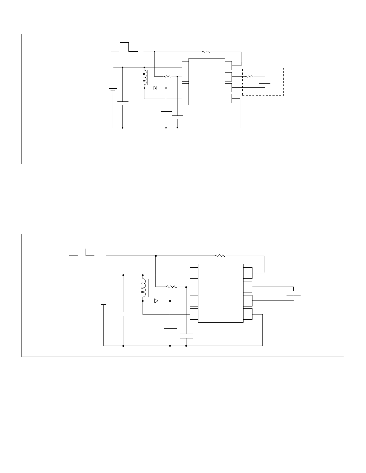
Figure 1: Test Circuit, VIN = 3.0V
ON = V
DD
OFF = 0V
1
220µH
VDD = VIN = 3.0V
Notes:
1. Murata part # LQH4N221K04 (DC resistance < 5.4Ω)
2. Larger values may be required depending upon supply impedance.
For additional information, see Application Notes AN-H33 and AN-H34.
Enable/Disable Configuration
0.1µF
BAS21LT1
2
0.01µF
200V
1MΩ
1
2
3
4
1nF
V
DD
R
SW-osc
C
s
L
x
5.1MΩ
R
EL-osc
GND
HV830
HV830
8
V
A
7
V
B
6
5
10 square inch lamp.
The HV830 can be easily enabled and disabled via a logic control
signal on the R
The control signal can be from a microprocessor. R
and REL resistors as shown in Figure 2 below.
SW
SW
and R
EL
peres will be drawn from the logic signal when it is at a logic high
(enable) state. When the microprocessor signal is high the
device is enabled and when the signal is low, it is disabled.
are typically very high values. Therefore, only 10’s of microam-
Figure 2: Enable/Disable Configuration
ON =V
DD
OFF = 0V
VIN = V
+
DD
-
Remote
Enable
4.7µF
15V
L
x
BAS21LT1
C
S
200V
1
R
SW
2
3
4
1nF
R
EL
DD
SW-osc
s
x
R
V
R
C
L
HV830LG
EL-osc
V
V
GND
8
A
7
EL Lamp
B
6
5
Split Supply Configuration Using a Single
Cell (1.5V) Battery
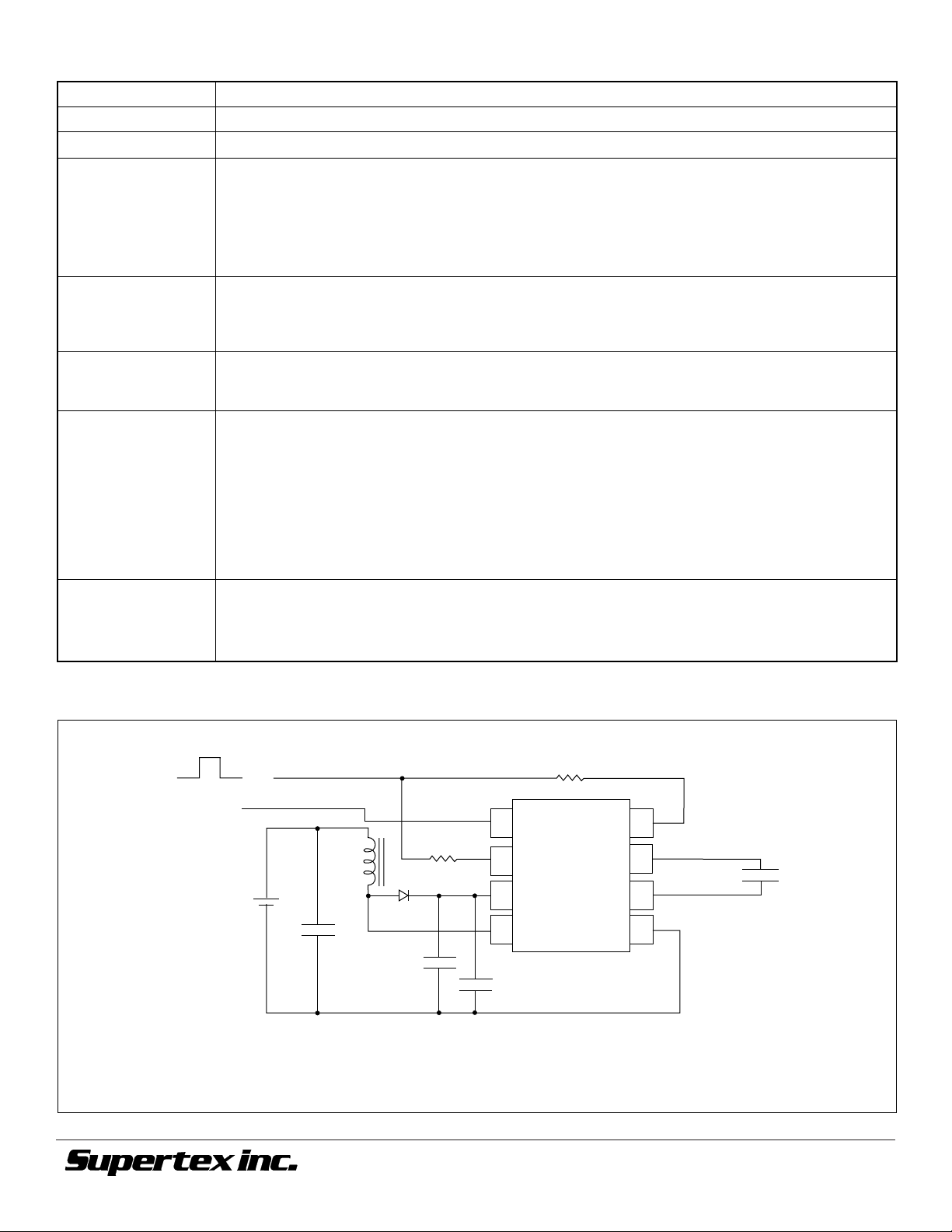
The HV830 can also be used for handheld devices operating
from a single cell 1.5V battery where a regulated voltage is
available. This is shown in Figure 3. The regulated voltage can
be used to run the internal logic of the HV830. The amount of
current necessary to run the internal logic is typically 100µA
at a V
provide the current without being loaded down. The HV830
used in this configuration can also be enabled/disabled via
logic control signal on the R
Figure 2.
of 3.0V. Therefore, the regulated voltage could easily
DD
and REL resistors as shown in
SW
Split Supply Configuration for Battery
Voltages of Higher than 9.5V
Figure 3 can also be used with high battery voltages such as 12V
as long as the input voltage, V
its specifications of 2.0V to 9.5V.
3
, to the HV830 device is within
DD
Page 4
HV830
External Component Description
External Component Selection Guide Line
Diode Fast reverse recovery diode, BAS21LT1 or equivalent.
Cs Capacitor 0.01µF to 0.1µF, 200V capacitor to GND is used to store the energy transferred from the inductor.
R
EL-osc
R
SW-osc
CSW Capacitor A 1nF capacitor is recommended on R
Lx Inductor The inductor Lx is used to boost the low input voltage by inductive flyback. When the internal switch is on,
Lamp As the EL lamp size increases, more current will be drawn from the battery to maintain high voltage across
The EL lamp frequency is controlled via an external REL resistor connected between R
device. The lamp frequency increases as R
of current drawn from the battery will increase and the output voltage V
decreases. As the EL lamp frequency increases, the amount
EL
will decrease. The color of the EL
CS
and VDD of the
EL-osc
lamp is dependent upon its frequency.
A 3.3MΩ resistor would provide lamp frequency of 220 to 280Hz. Decreasing the R
by a factor of 2 will
EL-osc
increase the lamp frequency by a factor of 2.
The switching frequency of the converter is controlled via an external resistor, RSW between R
SW-osc
and V
of the device. The switching frequency increases as RSW decreases. With a given inductor, as the switching
frequency increases, the amount of current drawn from the battery will decrease and the output voltage, V
will also decrease.
to GND when a 0.01µF CS capacitor is used. This capacitor
is used to shunt any switching noise that may couple into the R
SW-osc
pin. The CSW capacitor may also be
SW-osc
needed when driving large EL lamp due to an increase in switching noise.
the inductor is being charged. When the internal switch is off, the charge stored in the inductor will be
transferred to the high voltage capacitor CS. The energy stored in the capacitor is connected to the internal
H-bridge and therefore to the EL lamp. In general, smaller value inductors, which can handle more current,
are more suitable to drive larger size lamps. As the inductor value decreases, the switching frequency of the
inductor (controlled by R
) should be increased to avoid saturation.
SW
220µH Murata inductors with 5.4Ω series DC resistance is typically recommended. For inductors with the
same inductance value but with lower series DC resistance, lower RSW value is needed to prevent high current
draw and inductor saturation.
the EL lamp. The input power, (V
x IIN), will also increase. If the input power is greater than the power
IN
dissipation of the package (400mW), an external resistor in series with one side of the lamp is recommended
to help reduce the package power dissipation.
CS
DD
,
Figure 3: Split Supply Configuration
ON = V
DD
OFF = 0V
V
= Regulated
DD
Voltage
+
VIN = Battery
Voltage
*Larger values may be required depending upon supply impedance.
–
For additional information, see Application Notes AN-H33 and AN-H34.
©2001 Supertex Inc. All rights reserved. Unauthorized use or reproduction prohibited.
Remote
Enable
L
0.1µF*
x
BAS21LT1
C
S
200V
R
SW
4
1
2
3
4
1nF
V
R
C
L
R
EL
R
DD
SW-osc
s
x
EL-osc
GND
HV830LG
8
V
A
7
EL Lamp
V
B
6
5
11/12/01
1235 Bordeaux Drive, Sunnyvale, CA 94089
TEL: (408) 744-0100 • FAX: (408) 222-4895
www.supertex.com
 Loading...