

Page 1
HV7121B
Semiconductor Inc.
System IC SBU
DESCRIPTION
HV7121B is a highly integrated single chip CMOS color image sensor using Hynix 0.5um CMOS process
developed for image application to realize high efficiency R/G/B photo sensor. The sensor has 414X314 pixels
total, and 400X300 pixels effective. Each pixel is high photo sensitive, small size active pixel element that
converts photons to analog voltage signal. The sensor has three on-chip 8 bit Digital to Analog Convert (DAC)
and 414 comparators to digitize the pixel output. The three on-chip 8 bit DAC can be used for independent
R/G/B gain control. Hynix proprietary on-chip Correlated Double Sampling (CDS) circuit can reduce Fixed
Pattern Noise (FPN) dramatically. The whole 8 bit digital color raw data is directly available on the package
pins and just a few control signals are needed for whole chip control, so it is very ease to configure a system
using the sensor.
CMOS IMAGE SENSOR
With 8-bit ADC
FEATURES
l 400 x 300 pixels resolution l Full function control through standard I2C bus
l 8um x 8um square pixel l Built-in Automatic Gain Control (AGC)
l High efficiency R/G/B color photo sensors l 48 pin CLCC
l Integrated 8-bit ADC for direct digital output l Bayer RGB color pattern
l Low power 3.3V operation (5V tolerant I/O) l Anti-blooming circuit
l Integrated pan control and window sizing l Flexible exposure time control
l Clock speed up to 15MHz l Integrated on-chip timing and drive control
l Programmable frame rate and synchronous format l 1/4" optical format
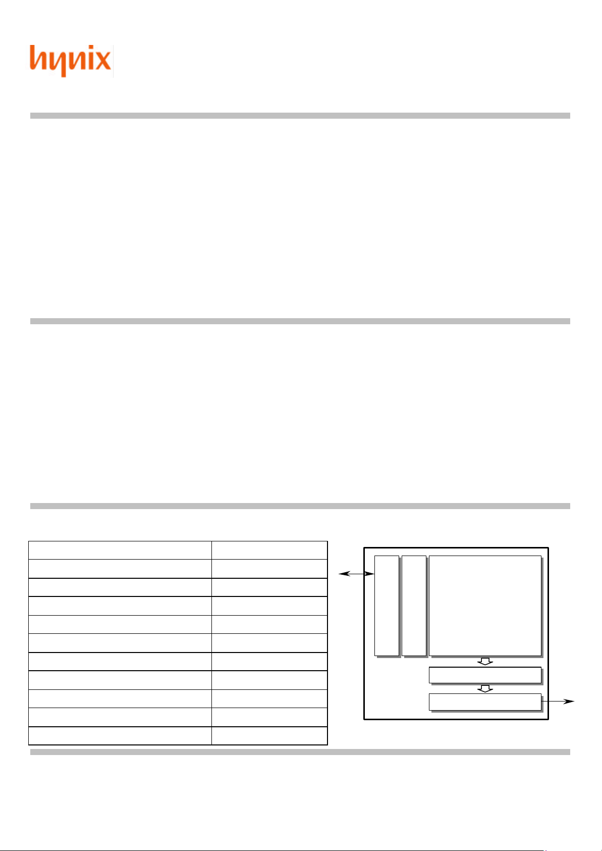
TECHNICAL SPECIFICATION FUNCTIONAL BLOCK DIAGRAM
Pixel resolution 402x302
Pixel size 8x8um
2
Fill factor 30%
Format CIF
Sensitivity 2.5V/luxžsec
Supply voltage for analog 3.3V
Supply voltage for digital 3.3V
Supply voltage for 5V tolerant input 5.0V
I2C
Pixel Array
Decoder/Pixel Driver
Control Register & Logic
ADC Block
Power Consumption
@15MHz
Line Buffer
Operating temperature 0~40 Centigrade
Technology 0.5um 3metal CMOS
This document is a general product description and is subject to change without notice. Hynix Semiconductor does not assume any
responsibility for use of circuits described. NO patent licenses are implied.
DA21000601R_1.1 - 1 - 2001 Hy nix System IC SBU
Page 2
HV7121B
Semiconductor Inc.
System IC SBU
ELECTRICAL CHARACTERISTICS
Absolute Maximum Ratings
l Supply voltage(Analog, Digital) : 3.0 V ~ 3.6 V
l Voltage on any input pins : 0 V ~ 5.0 V
l Operating Temperature(Centigrade) : 0 ~ 40
l Storage Temperature(Centigrade) : -30 ~ 80
Note : Input pins are 5V tolerant. Stresses exceeding the absolute maximum ratings may induce failure.
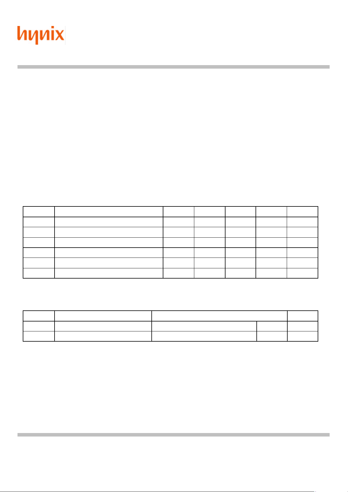
DC Operating Conditions
CMOS IMAGE SENSOR
With 8-bit ADC
Symbol Parameter Units Min. Max. Load[pF] Notes
Vdd Internal operation supply voltage Volt 3.0 3.6
Vih Input voltage logic "1" Volt 2.0 5 6.5
Vil Input voltage logic "0" Volt 0 0.8 6.5
Voh Output voltage logic "1" Volt 2.15 3.6 60
Vol Output voltage logic "0" Volt 0.4 0.4 60
Ta Ambient operating temperature Celsius 0 40
AC Operating Conditions
Symbol Parameter Max Operation Frequency Units Notes
MCLK Main clock frequency 20 MHz 1
SCK I2C clock frequency 400 KHz 2
1. MCLK can be divided according to Clock Divide Register for internal clock.
2. SCK is driven by host processor. For the detail serial bus timing, refer to I
2
C Spec.
This document is a general product description and is subject to change without notice. Hynix Semiconductor does not assume any
responsibility for use of circuits described. NO patent licenses are implied.
DA21000601R_1.1 - 2 - 2001 Hy nix System IC SBU
Page 3
HV7121B
Semiconductor Inc.
System IC SBU
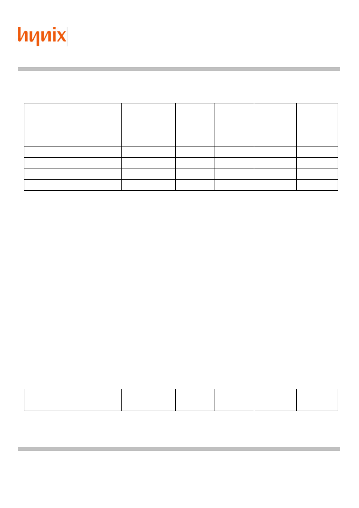
ELECTRO-OPTICAL CHARACTERISTICS
Color temperature of light source: 3200K / IR cut-off filter (CM-500S, 1mm thickness) is used. --- 8)
Parameter Units Min. Typical Max. Note
Sensitivity mV / luxžsec 1600 2500 1)
Dark Signal mV/sec 5 100 2)
Output Saturation Signal mV 1200 1250 3)
Dynamic Range dB 48 4)
Output Signal Shading % 8 13 5)
Dark Signal Shading mV/sec 3 300 6)
Frame Rate fps 60 7)
CMOS IMAGE SENSOR
With 8-bit ADC
Note:
1) Measured at 28lux illumination for exposure time 10 ms.
2) Measured at zero illumination for exposure time 50 ms. (T
3) Measured at Vdd =3.3V and 100lux illumination for exposure time 50msec.
4) 48dB is limited by 8-bit ADC.
5) Variance of average value of 4x4 pixels response of each block over all equal blacks at 50%
6) Range between V
7) Measured at MCLK 15MHz.
8) We recommend the IR cut-off filter with transmittance 50% at cut-off frequency 650nm for the real
Soldering
= 40 Centigrade)
temp
saturation level illumination for exposure time 10msec.
max
and V
at zero illumination for exposure time 50msec, where V
min
max
and V
are the maximum and minimum values of each block’s response, respectively.
Integration time must be set in order for effective window height not to exceed window height.
It ’s because effective window height is directly proportional to integration time.
applications.
min
Infrared(IR) / Convection solder reflow condition
Parameter Units Min. Typical Max. Note
Peak Temperature Range Celsius - 230 240 1)
Note:
1) Time within 5 Celsius of actual peak temperature, 10sec
This document is a general product description and is subject to change without notice. Hynix Semiconductor does not assume any
responsibility for use of circuits described. NO patent licenses are implied.
DA21000601R_1.1 - 3 - 2001 Hy nix System IC SBU
Page 4
MCLK
HV7121B
Semiconductor Inc.
System IC SBU
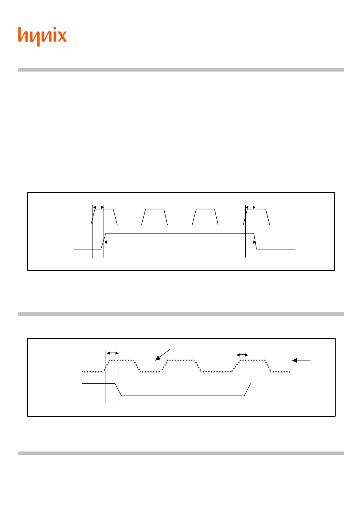
INPUT / OUTPUT AC CHARACTERISTICS
l All output timing delays are measured with output load 60[pF].
l Output delay include the internal clock path delay 6[ns] and output driving delay that changes in
respect to the output load, the operating environment, and a board design.
l Due to the variable valid time delay of the output, output signals may be latched in the negative
edge of MCLK for the stable data transfer between the image sensor and a host for less than
15MHz operation.
MCLK to HSYNC/VSYNC Timing
MCLK
T
1
T1
CMOS IMAGE SENSOR
With 8-bit ADC
HSYNC/VSYNC
T2
T1 : MCLK rising to HSYNC/VSYNC valid maximum time : 18ns [output load: 60pF]
T2 : HSYNC/VSYNC valid time : minimum 1clock(subject to T1, T2 timing rule)
MCLK to DATA Timing
T3
PCLK
T3
DATA[7:0]
valid data
T3 : MCLK rising to DATA valid maximum time : 18ns [output load: 60pF]
Note) HSYNC signal is high when valid data is on the DATA bus.
This document is a general product description and is subject to change without notice. Hynix Semiconductor does not assume any
responsibility for use of circuits described. NO patent licenses are implied.
DA21000601R_1.1 - 4 - 2001 Hy nix System IC SBU
Page 5
Semiconductor Inc.
System IC SBU
INPUT / OUTPUT AC CHARACTERISTICS (Continue)
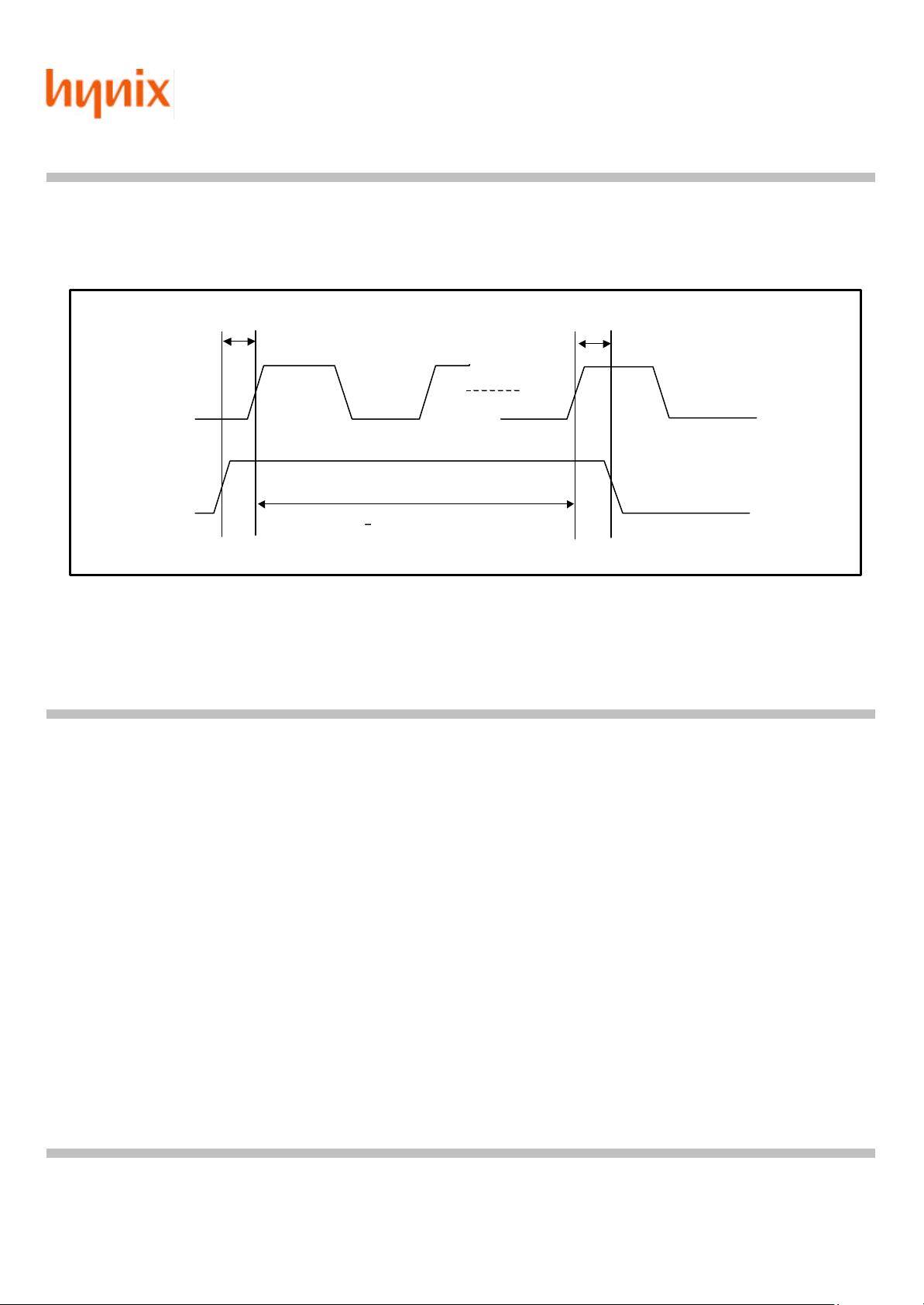
ENB Timing
HV7121B
CMOS IMAGE SENSOR
With 8-bit ADC
MCLK
T4
ENB
T4 : ENB Setup Time : 5[ns]
T5 : ENB Hold Time : 5 [ns]
T6 : ENB valid Time : minimum 2 clock
RESET Timing
T5
T6
Must in Valid (active low) state at least 8 MCLK periods
This document is a general product description and is subject to change without notice. Hynix Semiconductor does not assume any
responsibility for use of circuits described. NO patent licenses are implied.
DA21000601R_1.1 - 5 - 2001 Hy nix System IC SBU
Page 6
Semiconductor Inc.
System IC SBU
INPUT / OUTPUT AC CHARACTERISTICS (Continue)
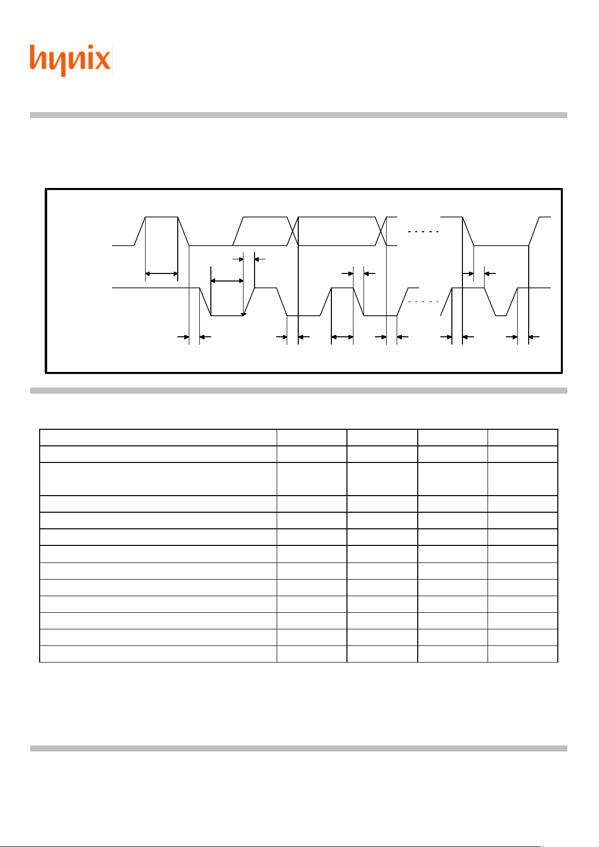
I2C Bus (Programming Serial Bus) Timing
stop start
HV7121B
CMOS IMAGE SENSOR
With 8-bit ADC
stopstart
SDA
SCK
tbuf
tlow
thd;sta
I2C Bus Interface Timing
Parameter Symbol Min. Max. Unit
SCK clock frequency f
Time that I2C bus must be free before a new
transmission can start
Hold time for a START thd;sta 1.0 us
LOW period of SCK t
HIGH period of SCK t
Setup time for START tsu;sta 1.2 us
tr
tf
thd;dat thigh tsu;dat tsu;sta tsu;sto
0 400 KHz
sck
t
1.2 us
buf
1.2 us
low
1.0 us
high
thd;sta
Data hold time thd;dat 1.3 us
Data setup time tsu;dat 250 ns
Rise time of both SDA and SCK tr
250 ns
Fall time of both SDA and SCK tf 300 ns
Setup time for STOP tsu;sto 1.2 us
Capacitive load of each bus lines(SDA,SCK) Cb pf
This document is a general product description and is subject to change without notice. Hynix Semiconductor does not assume any
responsibility for use of circuits described. NO patent licenses are implied.
DA21000601R_1.1 - 6 - 2001 Hy nix System IC SBU
Page 7
Semiconductor Inc.
System IC SBU
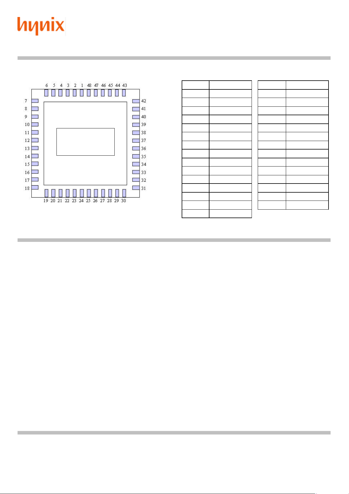
PIN CONFIGURATION (48 pin CLCC)
TOP VIEW
Pin9~16, Pin19~20, Pin33~41 : No Connection
PIN NO.
1 SCK
2 DGND
3 ENB
4 DGND
5 MCLK
6 VDD5
7 AVDD
8 AGND
17 AGND
18 AVDD
21 DGND
22 DATA7
23 DATA6
24 DATA5
25 DATA4
NAME
HV7121B
CMOS IMAGE SENSOR
With 8-bit ADC
PIN NO.
26 DGND
27 DATA3
28 DATA2
29 DATA1
30 DATA0
31 DVDD
32 DGND
42 DVDD
43 RESET
44 VSYNC
45 HSYNC
46 DGND
47 SDA
48 DGND
NAME
This document is a general product description and is subject to change without notice. Hynix Semiconductor does not assume any
responsibility for use of circuits described. NO patent licenses are implied.
DA21000601R_1.1 - 7 - 2001 Hy nix System IC SBU
Page 8
Semiconductor Inc.
System IC SBU
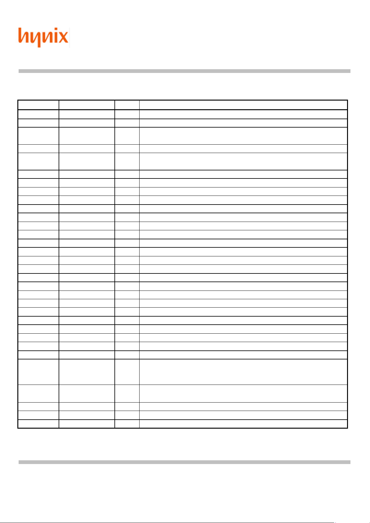
PIN DESCRIPTIONS (48 Pin CLCC)
PIN NAME I/O
1 SCK I I2C Clock ; I2C clock control from I2C master
2 DGND I Digital Ground
3 ENB I Sensor Enable Signal ; 'H' enable normal operation
'L' disable sensor
4 DGND I Digital Ground
5 MCLK I Master Clock (up to 15MHz)
; Global master clock for image sensor internal timing control
6 VDD5 I I/O bias voltage for 5V tolerant *1)
7 AVDD I Analog Supply Voltage 3.3V
8 AGND I Analog Ground
9 ~ 16 N.C No Connection
17 AGND I Analog Ground
18 AVDD I Analog Supply Voltage 3.3V
19, 20 Reserved Reserved
21 DGND I Digital Ground
22 DATA7 O Image Data bit 7
23 DATA6 O Image Data bit 6
24 DATA5 O Image Data bit 5
25 DATA4 O Image Data bit 4
26 DGND I Digital Ground
27 DATA3 O Image Data bit 3
28 DATA2 O Image Data bit 2
29 DATA1 O Image Data bit 1
30 DATA0 O Image Data bit 0
31 DVDD I Digital Supply Voltage 3.3V
32 DGND I Digital Ground
33 ~ 41 N.C No Connection
42 DVDD I Digital Supply Voltage 3.3V
43 RESET I Hardware Reset Signal, Active Low
44 VSYNC O Vertical synchronization signal / Frame start output
; Signal pulse at start of image data frame with programmable
blanking duration
45 HSYNC O Horizontal synchronization signal / Data valid output
/DVALID ; Data valid when 'H' with programmable blanking duration
46 DGND I Digital Ground
47 SDA I/O I2C Data ; I2C standard data I/O port
48 DGND I Digital Ground
DESCRIPTION
HV7121B
CMOS IMAGE SENSOR
With 8-bit ADC
*1) Tie to DVDD for 3.3V operation / Tie to 5V for 5V tolerant operation
This document is a general product description and is subject to change without notice. Hy nix Semiconductor does not assume
any responsibility for use of circuits described. NO patent licenses are implied.
DA21000601R_1.0 - 8 - 2001 Hynix System IC SBU
Page 9
HV7121B
Semiconductor Inc.
System IC SBU
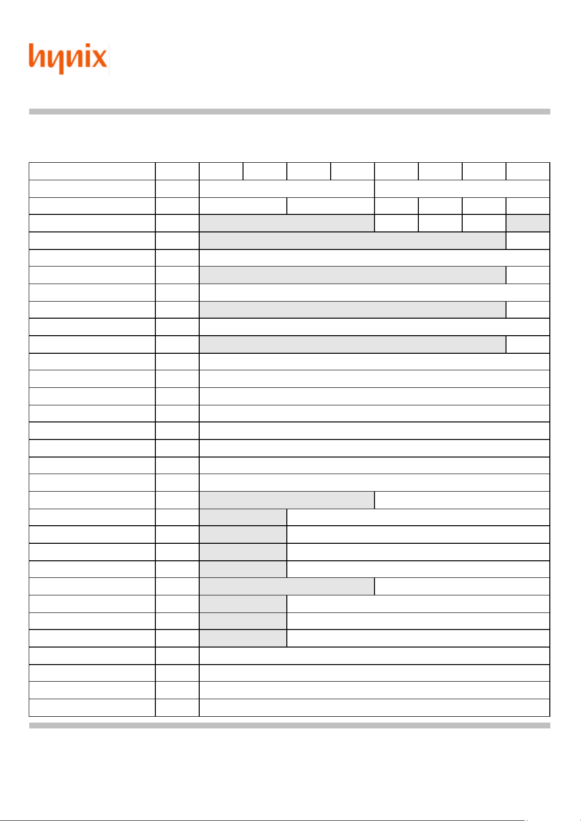
Register map
Register Name address 7 6 5 4 3 2 1 0
Mode A 00h model_name rev_num
Mode B 01h oper_mode data_type hs_out scr_size shot int_sel
Mode C 02h reserved sw_enb pwr_dn color reserved
Row Start Address High 10h reserved r_ad[8]
Row Start Address Low 11h r_ad[7:0]
Column Start Address High 12h reserved c_ad[8]
Column Start Address Low 13h c_ad[7:0]
Window Height Address High 14h reserved h_ad[8]
Window Height Address Low 15h h_ad[7:0]
CMOS IMAGE SENSOR
With 8-bit ADC
Window Width Address High 16h reserved w_ad[8]
Window Width Address Low 17h w_ad[7:0]
HSYNC Blanking Time High 20h h_blank[15:8]
HSYNC Blanking Time Low 21h h_blank[7:0]
VSYNC Blanking Time High 22h v_blank[15:8]
VSYNC Blanking Time Low 23h v_blank[7:0]
Integration Time Hig h 25h int_time[23:16]
Integration Time Middle 26h int_time[15:8]
Integration Time Low 27h int_time[7:0]
Master Clock Divider 28h reserved clk_div[3:0]
Reset Level Control 30h rst_level[5:0]
Red Color Gain 31h reserved red_color[5:0]
Green Color Gain 32h reserved green_color[5:0]
Blue Color Gain 33h reserved blue_color[5:0]
Pixel Bias Voltage 34h reserved pixel_bias[3:0]
Red Offset Gain Control 50h reserved red_offset[6:0]
Green Offset Gain Control 51h reserved green_offset[6:0]
Blue Offset Gain Control 52h reserved blue_offset[6:0]
Low Reference Number High 57h low_ref_no[15:8]
Low Reference Number Low 58h low_ref_no[7:0]
High Reference Number High 59h high_ref_no[15:8]
High Reference Number Low 5Ah high_ref_no[7:0]
This document is a general product description and is subject to change without notice. Hy nix Semiconductor does not assume
any responsibility for use of circuits described. NO patent licenses are implied.
DA21000601R_1.0 - 9 - 2001 Hynix System IC SBU
Page 10
HV7121B
Semiconductor Inc.
System IC SBU
Register Set Description s
All register access can though the I
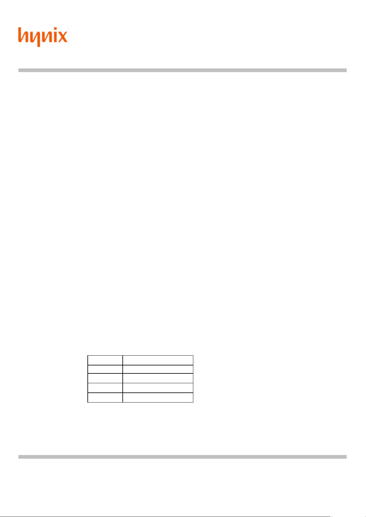
(1) Mode A Register (Address 00h, RO)
This register consist of a model name and revision number. The upper 4 bits is model_name [3:0] and
the lower 4 bits is rev_num[3:0]. For example it’s value 12h, this mean 400*300 resolution and
revision2.0 chip.
< model_name > < rev_num >
2
C multi-byte read and write.
CMOS IMAGE SENSOR
With 8-bit ADC
400*300 : 0001b Rev. 2.0 : 0010b
(2) Mode B Register (Address 01h, default : 04h, R/W)
This register defines major operation mode of the chip.
n Mode B[7:6] : oper_mode(operating mode) <default value : 00b>
Define operating modes between normal operation and optical and function test operation.
Test operation mode is used for optical and function test. Except for default value, these bits
are reserved for manufacturer.
Bit operating mode
00 Normal operation
01 Reserved
10 Reserved
11 Reserved
This document is a general product description and is subject to change without notice. Hy nix Semiconductor does not assume
any responsibility for use of circuits described. NO patent licenses are implied.
DA21000601R_1.0 - 10 - 2001 Hynix System IC SBU
Page 11
Semiconductor Inc.
System IC SBU
n Mode B [5:4] : data_type(data types) <default value : 00b>
These bits define output pixel data types. For Correlated Double Sampling(CDS), every the
pixel of image sensor are measured twice, reference and data respectively, and reference
values or data values can be read out through pixel data pins selectively using these control
bits. To remove the noise caused by circuit, i.e. Fixed Pattern Noise, the image sensor
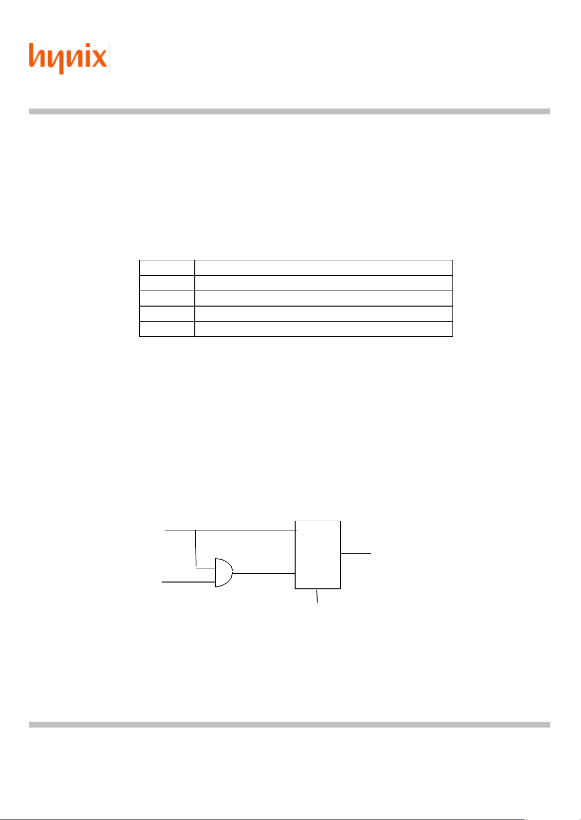
performs the CDS in default value. Three output data types are supported as follows.
Bit Output data type
00 Data level - Reference level
01 Reference level
10 Data level
11 Reserved
HV7121B
CMOS IMAGE SENSOR
With 8-bit ADC
n Mode B[3] : hs_out(HSYNC output configuration) <default value : 0b>
This bit offers two types output style about HSYNC signal. HSYNC only mode and HSYNC &
internal clock mode. If the hs_out is set to one, HSYNC output signal is ANDed signal of
internal pixel clock and data valid. Otherwise HSYNC output pin keep data high state during
valid output period. When HSYNC & internal clock mode is set, HSYNC output can be used
as a pixel data output clock.
data valid
MUX HSYNC
pixel clock
Mode B[3]
This document is a general product description and is subject to change without notice. Hy nix Semiconductor does not assume
any responsibility for use of circuits described. NO patent licenses are implied.
DA21000601R_1.0 - 11 - 2001 Hynix System IC SBU
Page 12

Semiconductor Inc.
System IC SBU
n Mode B[2] : scr_size(screen size select) <default value : 1b>
Flexible screen size is very useful for customer. If the scr_size is set to high, i.e. window
mode, only pixels in windowed area defined by register 10h ~ 17h can be read . But scr_size
is set to low state, i.e. full screen mode, all pixels in the sensor are read out regardless the
values of register 10h ~ 17h. We can select window mode or full screen mode with this bit. Full
screen size is only for chip test.
- window start point :
x : row start address (register 10h, 11h)
y : column start address (register 12h, 13h)
- window end point :
HV7121B
CMOS IMAGE SENSOR
With 8-bit ADC
x : row start address + window width address (register 14h, 15h) - 1
y : column start address + window height address (register 16h, 17h) –1
n Mode B [1] : shot(shot mode) <default value : 0b>
User can select continuous frame mode or snapshot mode according to application.
At the continuous frame mode, pixel data output is updated every VSYNC period. In order to
set snapshot mode, it this bit to ‘1’. In that case, just single frame of pixel data will be read out,
then the sensor stops operation. Snapshot mode can be used for the digital still camera
applications.
n Mode B[0] : int_sel(integration time unit select) <default value : 0b>
This bit defines integration time unit i.e. line base or pixel clock base.
Default mode is line unit integration but at the bright condition or if you need precise exposure
time control, pixel mode is recommended. This bit related to integration time register 25h, 26h,
and 27h.
<Note>
Actual integration time can be calculated using three integration time regis ters and main clock
period.
In pixel mode, integration time = (25h, 26h, 27h) * main clock period.
In line mode, integration time = (26h, 27h) * line period.
(cf) line period = 828 * main clock period
This document is a general product description and is subject to change without notice. Hy nix Semiconductor does not assume
any responsibility for use of circuits described. NO patent licenses are implied.
DA21000601R_1.0 - 12 - 2001 Hynix System IC SBU
Page 13

Semiconductor Inc.
System IC SBU
(3) Mode C Register (Address 02h, default : 08h, R/W)
This register controls power down and color select.
n Mode C[3] : sw_enb (software enable : active low)
(400*300 CMOS image sensor only) <default value : 1b>
This bit is only exist in 400*300 CMOS image sensor chip to enable image sensor operation
by software. This bit has same function as ENB pin control.
It’s very useful for the applications that is needed want to reduce interface pin count to
CMOS image sensor. In that case, cannot ENB pin to VDD line and control the sensor using
this bit.
HV7121B
CMOS IMAGE SENSOR
With 8-bit ADC
n Mode C[2] : pwr_dn(A/D converter power down) <default value : 0b>
This bit controls power down of A/D converter when sleep mode(idle state) is set by ENB pin
is low or sw_enb(Mode C[3]) is high. When set to high, A/D converter is turned on whenever
ENB is low or sw_enb is high. When set to low, A/D converter is turned off always regardless
ENB pin state or sw_enb state . But digital block goes to power down mode always when
ENB is low regardless this bit.
n Mode C[1] : color(color select) <default value : 0b>
This bit selects color mode or monochrome mode. Default value means color image sensor
and all three ADCs are used for Bayer RGB color pattern respectively, then RGB gains are
controlled independently. But when set this to one, i.e. monochrome mode, just single ADC is
used for all pixels regardless RGB color.
At the monochrome mode all pixels are controlled by ‘G’ gain only. ‘R’ and ‘B’ gain are not
used. In case of monochrome image sensor, this bit should be set to ‘1’ get the good image
and to simplify the sensor control.
(4) Row start address Register
(Higher byte : Address 10h, default : 00h, R/W)
(Lower byte : Address 11h, default : 06h, R/W)
Define window start position row start address of display window. Should be programmed with
value between 6 and 306.
This document is a general product description and is subject to change without notice. Hy nix Semiconductor does not assume
any responsibility for use of circuits described. NO patent licenses are implied.
DA21000601R_1.0 - 13 - 2001 Hynix System IC SBU
Page 14

Semiconductor Inc.
System IC SBU
(5) Column start address Register
(Higher byte : Address 12h, default : 00h, R/W)
(Lower byte : Address 13h, default : 06h, R/W)
Define window start position column address of display window. Should be programmed wi th value
between 6 and 406.
(6) Window Height address Register
(Higher byte : Address 14h, default : 01h, R/W)
(Lower byte : Address 15h, default : 2Eh, R/W)
Define display window height. If you need smaller display window height, decrease the value.
HV7121B
CMOS IMAGE SENSOR
With 8-bit ADC
Window end position row address = row start address + window height address –1
(7) Window width address Register
(Higher byte : Address 16h, default : 01h, R/W)
(Lower byte : Address 17h, default : 92h, R/W)
Define display window width. If you need smaller display window width, decrease the value.
Window end position column address = column start address + window width address -1
Note : Display window programming.
< Display Window Programming >
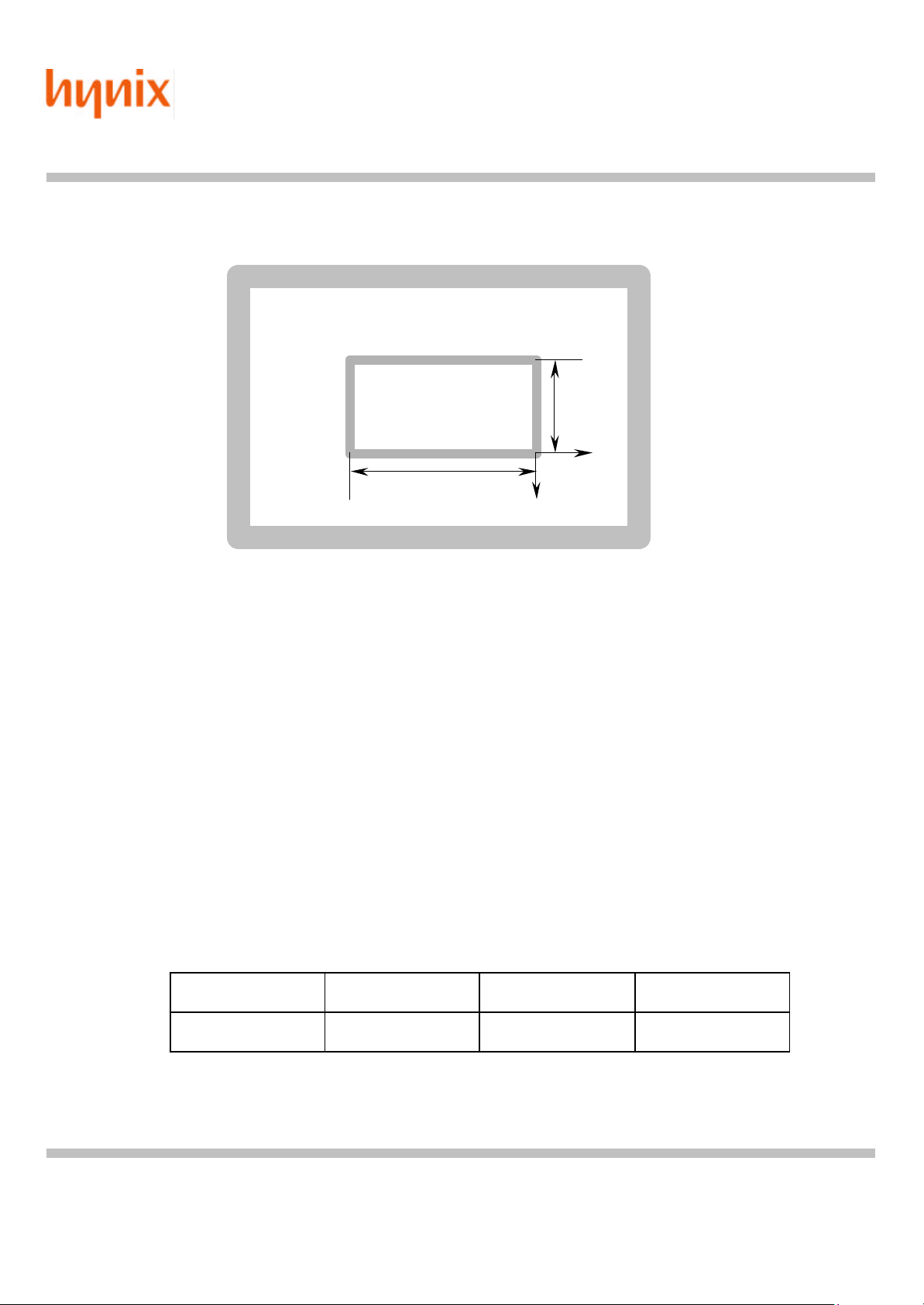
The 400*300 resolution chip can read any user specific window area within active window area.
This is called panning function. For this function, ‘row start’, ‘column start’, ‘width’, and ‘height’
can be programmed with four sets of register pair.
n FRS : Frame Row Start
n FCS : Frame Column Start
n FWH : Frame window Height
n FWW : Frame Window Width
This document is a general product description and is subject to change without notice. Hy nix Semiconductor does not assume
any responsibility for use of circuits described. NO patent licenses are implied.
DA21000601R_1.0 - 14 - 2001 Hynix System IC SBU
Page 15
Semiconductor Inc.
FRSU, FRSL
System IC SBU
Panning window can be programmed as below.
HV7121B
CMOS IMAGE SENSOR
With 8-bit ADC
(413,313)
(0,313)
(407,307)
{FWWU, FWWL}
{FWHU, FWHL}
{FRSU, FRSL}
{FCSU, FCSL}
(6,6)
(413,0)
(0,0)
Note 1) Accessible pixel array size is 402*302.
The edge of accessible pixel array may be commonly dedicated for just color interpolation.
In the case of a color image sensor the interpolation is needed to get all R,G,B color value for
each pixel from a Bayer color image.
So one more extra pixel line is needed at the edge of pixel array that you want to be displayed.
That is, to make 400*300 effective window, 402*302 pixel array necessary.
You have to consider this interpolation line when you program the ‘Frame register’.
For example, if you want to get 300*250 image size, you have to program 302*252 to frame
register.
<Default window area>
6 FWHU, FWHL 302
FCSU, FCSL 6 FWWU, FWWL 402
This document is a general product description and is subject to change without notice. Hy nix Semiconductor does not assume
any responsibility for use of circuits described. NO patent licenses are implied.
DA21000601R_1.0 - 15 - 2001 Hynix System IC SBU
Page 16
Semiconductor Inc.
System IC SBU
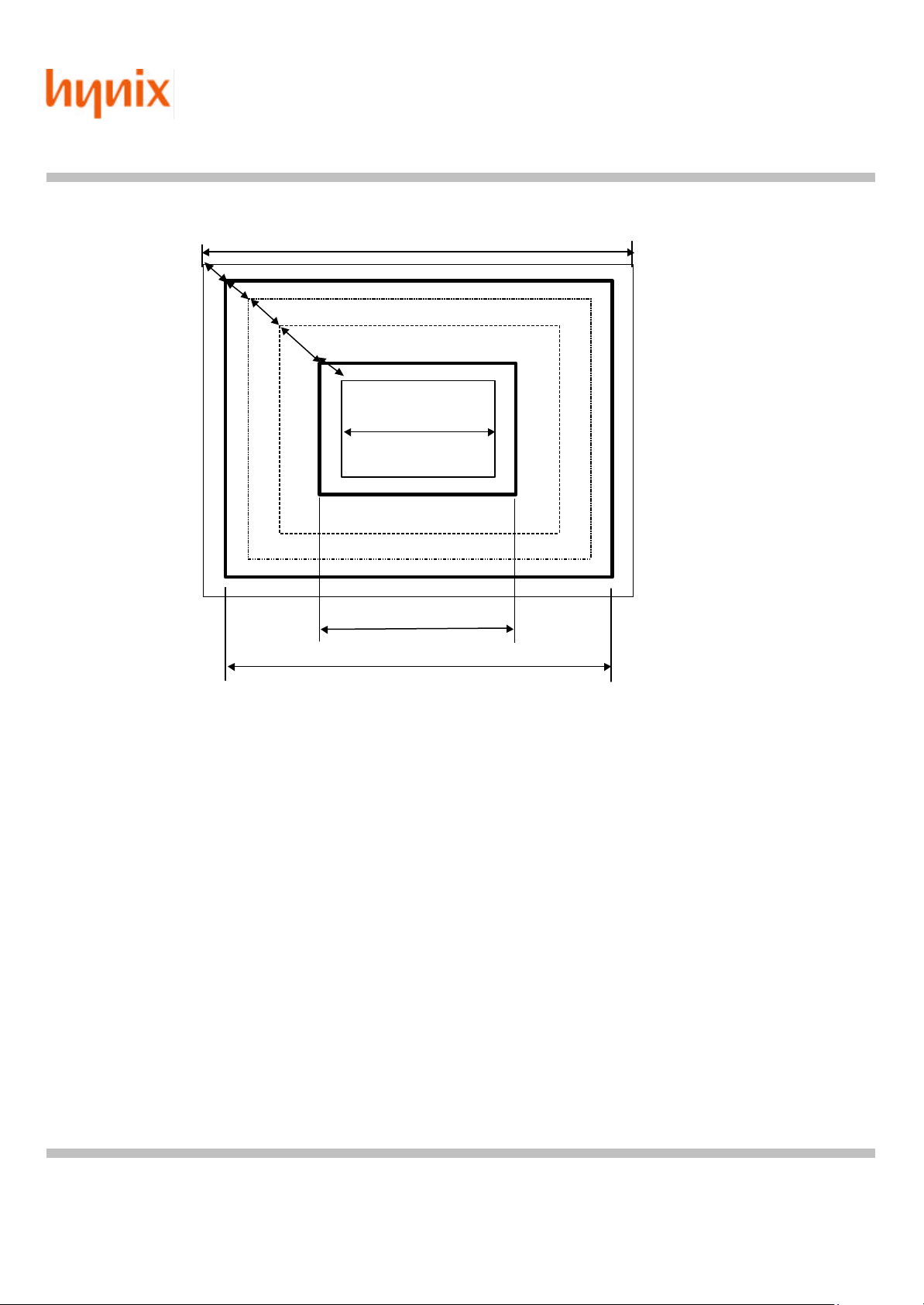
< Pixel Array Structure >
total pixel : 416 * 316
+1 : dummy area
+1 : dummy zone for set of color pattern
+1 : interpolation area
+2 : optical block zone
+3 : margin for metal 3 slope
HV7121B
CMOS IMAGE SENSOR
With 8-bit ADC
pixel array : 400 * 300
R
G - - - -
- - - -
B G G B
R
G
G B
R G
active window area (402 * 302)
accessible address range(414 * 314)
(8) HSYNC Blanking Time Register
(Higher byte : Address 20h, default : 00h, R/W)
(Lower byte : Address 21h, default : 03h, R/W)
HSYNC low duration is HSYNC blanking time plus (828-2*window width)*main clock period.
It’s used to change duration between current line end and next line start.
This document is a general product description and is subject to change without notice. Hy nix Semiconductor does not assume
any responsibility for use of circuits described. NO patent licenses are implied.
DA21000601R_1.0 - 16 - 2001 Hynix System IC SBU
Page 17

Semiconductor Inc.
System IC SBU
(9) VSYNC Blanking Time Register
(Higher byte : Address 22h, default : 00h, R/W)
(Lower byte : Address 23h, default : 03h, R/W)
The VSYNC blank, and time defines VSYNC active duration in pixel unit .
<Note>
HSYNC blanking, VSYNC blank are used to fit the CMOS sensor display timing to external timing
requirements.
(10) Integration time Register
HV7121B
CMOS IMAGE SENSOR
With 8-bit ADC
(High byte : Address 25h, default : 00h, R/W)
(Middle byte : Address 26h, default : 01h, R/W)
(Low byte : Address 27h, default : f4h, R/W)
Each pixel has a photo diode in which the incoming photons are converted to electrons. Integration
time mean exposure time so these registers defines exposure time.
According to settings int_sel of Mode B register, the integration time is controlled with line or pixel
unit. Small value means short exposure time and large value means long exposure time for bright
condition.
The value should be large for dark condition. Default value setting 500 lines, this value is useful for
normal office condition. If you stay in outdoor condition, this value should be decreased. But under
dark condition, this value should be increased to get a good image quality. Increasing value may
decrease frame rate. Finally, integration time is very important for frame rate and image quality.
For line mode exposure, register 26h and 27h are used. For pixel mode exposure, all three register
25h ~ 27h are used. To control exposure time precisely, the pixel mode should be used. This register
may be used for Auto Exposure control.
This document is a general product description and is subject to change without notice. Hy nix Semiconductor does not assume
any responsibility for use of circuits described. NO patent licenses are implied.
DA21000601R_1.0 - 17 - 2001 Hynix System IC SBU
Page 18
HV7121B
Semiconductor Inc.
System IC SBU
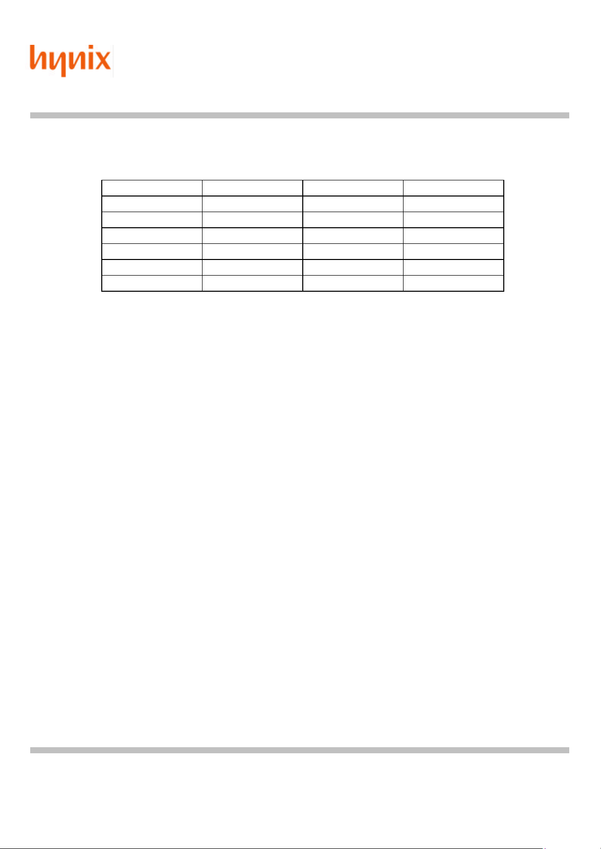
(11) Operating Clock Divider (Address 28h, default:00h, R/W)
This register generates divided digital clock depending on the settings clk_div [3:0], digital block can
divide MCLK down by 1 through 2048 as shown in Table 1.
clk_div[3:0] units clk_div[3:0] units
0000 no division 0101 MCLK/64
0001 MCLK/2 0111 MCLK/128
0010 MCLK/4 1000 MCLK/256
0011 MCLK/8 1001 MCLK/512
0100 MCLK/16 1010 MCLK/1024
0101 MCLK/32 1011 MCLK/2048
Table 1. Operating Clock Control Register
(12) Reset Level Control Register (Address 30h, default:38h, R/W)
CMOS IMAGE SENSOR
With 8-bit ADC
This register controls reference voltage level for start point of data reading. If the register value is
too large or too small, the vertical Fixed Pattern Noise(FPN) can be occurred. To Get rid of FPN,
this register must have a suitable value. Optimum reset level can be found using Low reference
number registers 57h ~ 58h and High reference number registers 59h ~ 5ah. If there is some large
value in Low reference number registers, the value of Reset Level control register should be
increased. If there is some large value in High reference number registers, the value of register
should be decrease. Optimum reset level is achieved when value of Low reference level number
registers and value of High reference number registers is minimized.
(13) Color Gain Register
Red Color Gain Register : (Address 31h, default : h1Eh, R/W)
Green Color Gain Register : (Address 32h, default : h1Eh, R/W)
Blue Color Gain Re gister : (Address 33h, default : h1Eh, R/W)
These registers are used to amplify the analog pixel output. If the gain register value is decreased,
the amplification is increased. Therefore under the dark light source condition, the pixel output have
to be amplified by decreasing gain value to get good image. There are three Gain registers to control
RGB colors independently. In the case of monochrome image sensor, use only Green Color Gain
Register. Available program range is 0 ~ 63 but too small value can cause FPN. The register value
have to chosen within the range that doesn’t cause FPN. Recommended range is 20 ~63. These
register can be used for Auto White Balance control and Auto Exposure control.
This document is a general product description and is subject to change without notice. Hy nix Semiconductor does not assume
any responsibility for use of circuits described. NO patent licenses are implied.
DA21000601R_1.0 - 18 - 2001 Hynix System IC SBU
Page 19

Semiconductor Inc.
System IC SBU
(14) Pixel Bias Voltage Register (Address 34h, default:02h, R/W)
This register controls pixel reference level by controlling bias current of pixel output sensing load
transistor. It controls pixel output level itself, compare with that revel register adjust A/D Converter
circuit to calibrate reference level for data reading. Available program range is 0 ~ 7. The larger
register value causes the higher bias current and low pixel output reference level. This register is
option for manufacturer. Users may use default setting and don’t changed value.
(15) Low Reference Number Register(low_ref_no)
High : (Address 57h default : 00h, Read Only)
Low : (Address 58h, default : 00h, Read Only)
HV7121B
CMOS IMAGE SENSOR
With 8-bit ADC
Low Reference Number Registers indicates number of pixels in frame that have a value less then 5.
A reference level values of each pixel is compare with ‘5’, and accumulated to these registers
during read state. This counter value called low_ref_no, consist of two bytes and it is read only
registers. Real number of pixels that have value less than 5 is the twice of these register value. If
low_ref_no is big value, you must increase data value of Reset Level Control Register. These
registers are updated after every VSYNC signal.
(16) High Reference Number Register (high_ref_no)
High : (Address 59h, default:00h, Read Only)
Low : (Address 5Ah, default:00h, Read Only)
High Reference Number Registers indicates number of pixels in a frame that have a value great then
123. Reference level values of each pixels is compared with ‘123’, and accumulated to these
registers during read state. This counter value called high_ref_no, consist of two bytes and it is read
only registers. Real number of pixels that have value great than 123 is the twice of these register
value. If high_ref_no is big value, you must decrease data value of Reset Level Control Register.
These registers are also updated after every VSYNC signal.
This document is a general product description and is subject to change without notice. Hy nix Semiconductor does not assume
any responsibility for use of circuits described. NO patent licenses are implied.
DA21000601R_1.0 - 19 - 2001 Hynix System IC SBU
Page 20
HV7121B
SensorArrayHeight
SensorArrayWidth
RowStartAddress
WindowHeight
EffectiveWindowHeight
Semiconductor Inc.
System IC SBU
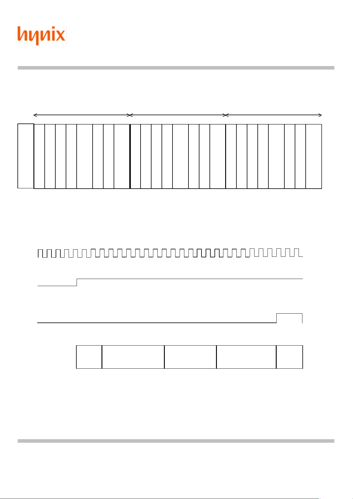
FRAME TIMING DIAGRAMS
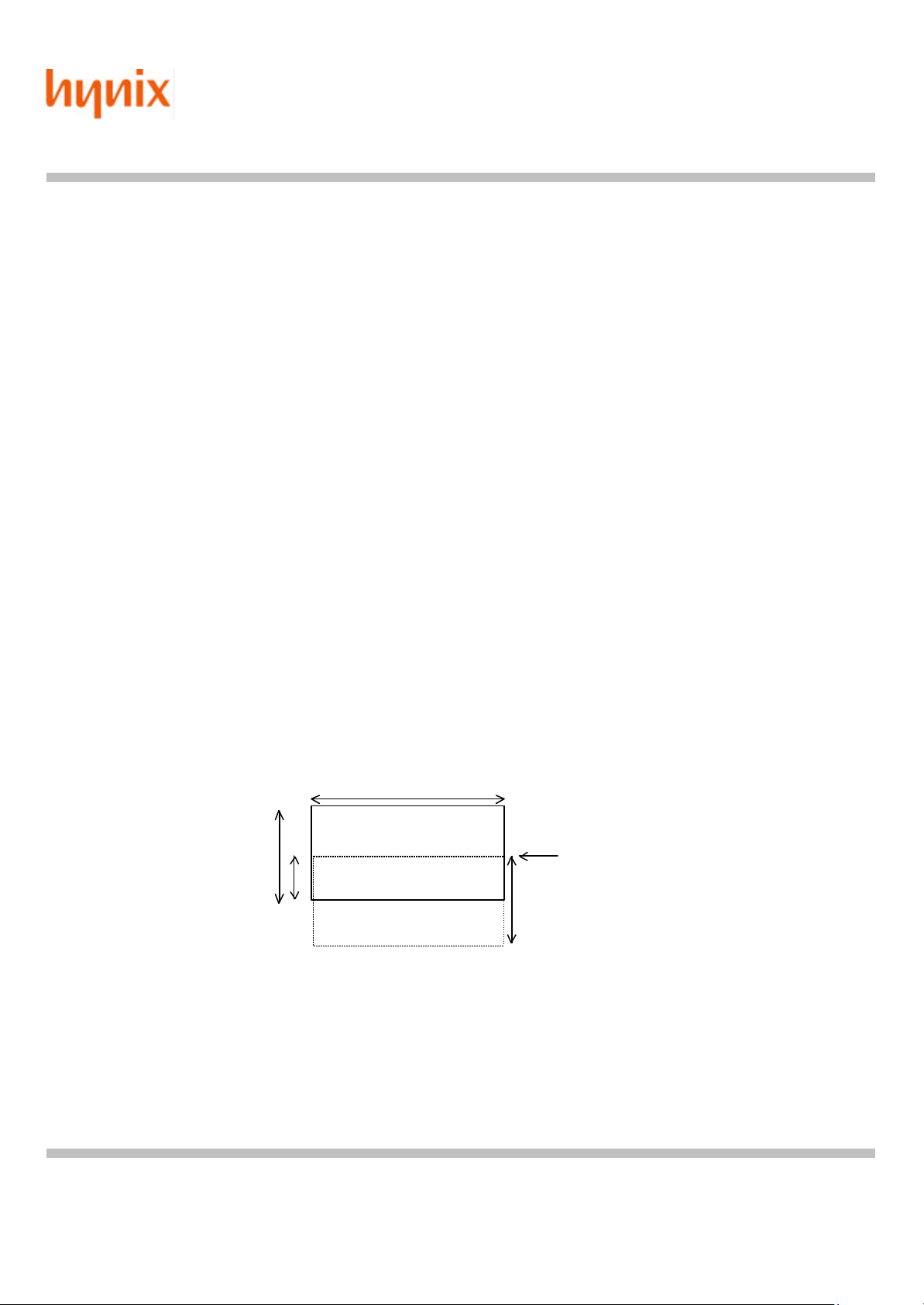
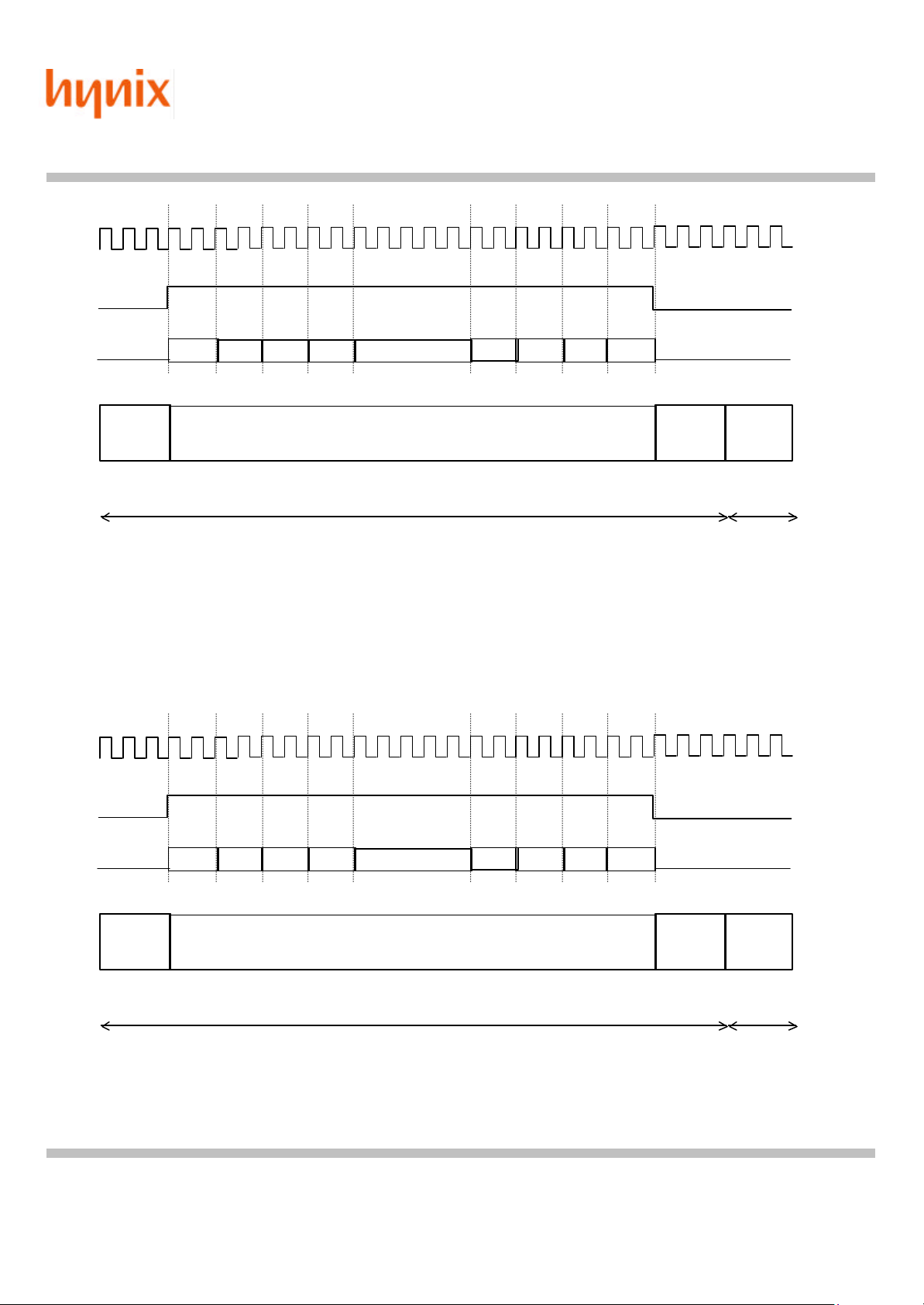
There are two frame timing cases,
l Integration Time < EffectiveWindowHeight * Scale
l Integration Time > EffectiveWindowHeight * Scale
EffectiveWindowHeight is equal to the number of data lines generated in a frame and is defined to be
selected by
if((RowStartAddress + WindowHeight + 1) <= (SensorArrayHeight)
EffectiveWindowHeight = WindowHeight;
else
EffectiveWidnowHeight = (SensorArrayHeight - RowStartAddress - 1);
CMOS IMAGE SENSOR
With 8-bit ADC
For example, RowStartAddress = 200 and WindowHeight = 300, EffectiveWindowHeight is 113 and 113
data lines per a frame are generated.
Note : The above selection logic is somewhat confusing in respect of general counting measure. It’s partly
due to the mixed use of indexing start points, i.e. ‘0’ and ‘1’ in the design. Therefore in order to avoid the
confusion it is desirable to just follows the equation when you estimate the frame rate.
[414]
(0,0)
[314]
[113]
[200]
[300]
Scale is selected according to Integration Time Mode by
If(PixelMode) Scale = SensorArrayWidth; // For400*300 resolution chip, SensorArrayWidth is 414
else Scale = 1;
This document is a general product description and is subject to change without notice. Hy nix Semiconductor does not assume
any responsibility for use of circuits described. NO patent licenses are implied.
DA21000601R_1.0 - 20 - 2001 Hynix System IC SBU
Page 21

HV7121B
Semiconductor Inc.
System IC SBU
When Integration Time > (EffectiveWindowHeight * Scale), next frame VSYNC does not follow immediately
after current frame’s last line has been produced. Instead, one of the following two idle time slots is inserted
according to Integration Time Mode before next frame VSYNC gets active.
< Idle Slots >
l Line Mode: (Integration Time - EffectiveWindowHeight) * 1024 clocks
l Pixel Mode: (Integration Time - EffectiveWindowHeight * Scale)
= (Integration Time - EffectiveWindowHeight * SensorArrayWidth) clocks
Each Frame Timing of the above cases may be decomposed into four timing segments
CMOS IMAGE SENSOR
With 8-bit ADC
l Initial Data Setup Time after ENB gets active
l Even Line
l Odd Line
l Frame Transition
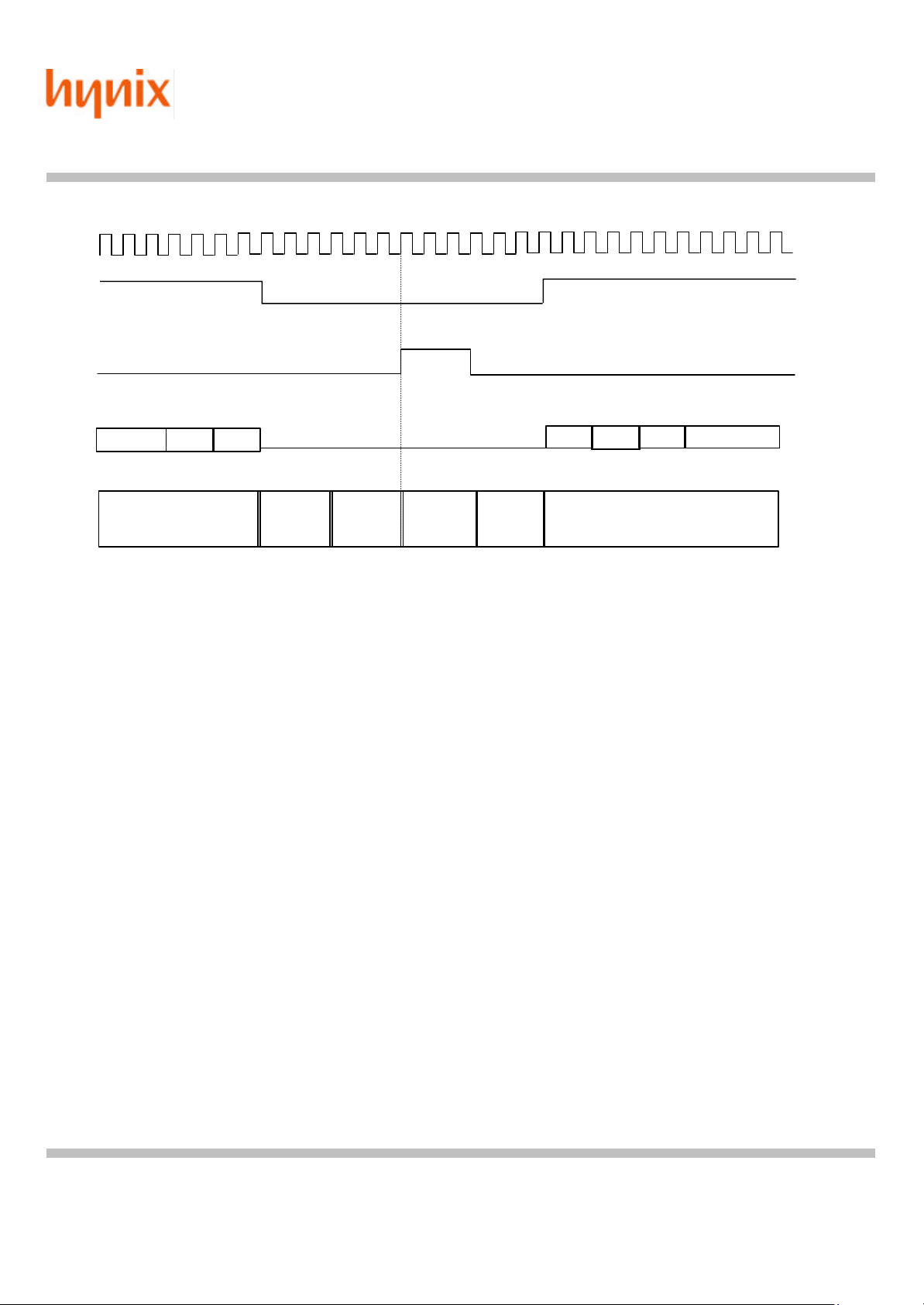
The subsections will describe frame timing diagram for said frame time cases, (Integration Time < Effective Window
Height * Scale) and (Integration Time > Effective Window Height * Scale)
(1) Frame Timing Diagram for Integration Time < (EffectiveWindowHeight * Scale)
Frame timing related registers are programmed to suit for the above condition as follows
RowStartAddress = 6; WindowHeight = 302;
ColumnStartAddress = 6; WindowWidth = 402;
IntegrationTime = 200 [Line Mode];
EffectiveWindowHeight is “302” for (SensorArrayHeight > (RowStartAddress + WindowHeight + 1)), i.e. 314 >
(6 + 302 + 1), is met, and Scale is “1” for integration time is line mode.
Therefore, (Integration Time< EffectiveWindowHeight * Scale), i.e. 200 < 302 * 1, is met.
This document is a general product description and is subject to change without notice. Hy nix Semiconductor does not assume
any responsibility for use of circuits described. NO patent licenses are implied.
DA21000601R_1.0 - 21 - 2001 Hynix System IC SBU
Page 22
Semiconductor Inc.
ENB+
Sensor Reset
One Line Time Delay
[417 clocks]
VSYNC
Integration Time *
Line 0
Line 1
Line 2
Line 300
Line 301
VSYNC
Line 0
Line 1
Line 2
Line 300
Line 301
VSYNC
Line 0
Line 1
Line 2
Line 300
Line 301
VSYNC
System IC SBU
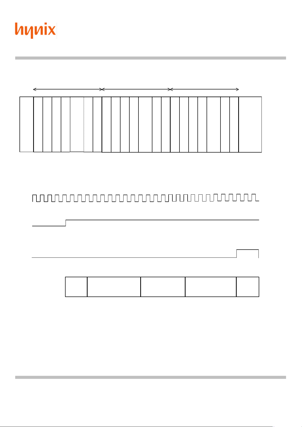
Overall Frames Sequence
HV7121B
CMOS IMAGE SENSOR
With 8-bit ADC
Initial Data Setup Time
MCLK
Frame 1 Frame 2 Frame 0
....
....
....
....
ENB
VSYNC
Delay
Slots
Deglitch
2 clocks
SensorArrayHeight clocks
[314 clocks]
Fig. 1 Initial Data Setup Time after ENB gets active
Scale clocks
[200 * 414 clocks]
(SensorArrayWidth +
HBLANK) clocks
3 clocks
This document is a general product description and is subject to change without notice. Hy nix Semiconductor does not assume
any responsibility for use of circuits described. NO patent licenses are implied.
DA21000601R_1.0 - 22 - 2001 Hynix System IC SBU
Page 23
Semiconductor Inc.
IMAGE RAW DATA
Line Head
HBLANK
G G B
Line Tail
SensorArrayWidth (828 )
HBLANK(3)
IMAGE RAW DATA
Line Head
HBLANK
R R G
Line Tail
SensorArrayWidth (828 )
HBLANK(3)
System IC SBU
MCLK
HSYNC
DATA
B⋅
HV7121B
CMOS IMAGE SENSOR
With 8-bit ADC
Time
Slot
Clock
Ruler
MCLK
HSYNC
DATA
Blank
12 clocks
Window Width
804 clocks
Fig.2 Even Line Data Timing
G⋅
Blank
12 clocks
3 clocks
Time
Slot
Blank
12 clocks
Window Width
804 clocks
Blank
12 clocks
3 clocks
Clock
Ruler
Fig.3 Odd Line Data Timing
This document is a general product description and is subject to change without notice. Hy nix Semiconductor does not assume
any responsibility for use of circuits described. NO patent licenses are implied.
DA21000601R_1.0 - 23 - 2001 Hynix System IC SBU
Page 24
Semiconductor Inc.
B B . . . . . . .
Line Tail
IMAGE RAW DATA
Line Head
G
. . . . .
IMAGE RAW DATA
VSYNC
≈
≈
HBLANK
System IC SBU
MCLK
HSYNC
VSYNC
DATA
HV7121B
CMOS IMAGE SENSOR
With 8-bit ADC
Time
Slot
Window Width
804 clocks
Blank
12 clocks
3 clocks
3 clocks
Blank
12 clocks
Window Width
804 clocks
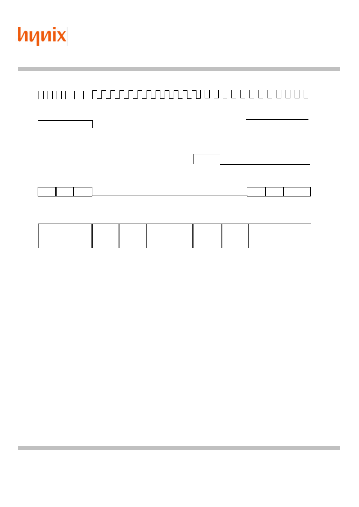
Integration Time < EffectiveWindowHeight * Scale
Fig.4 Frame Transition Timing
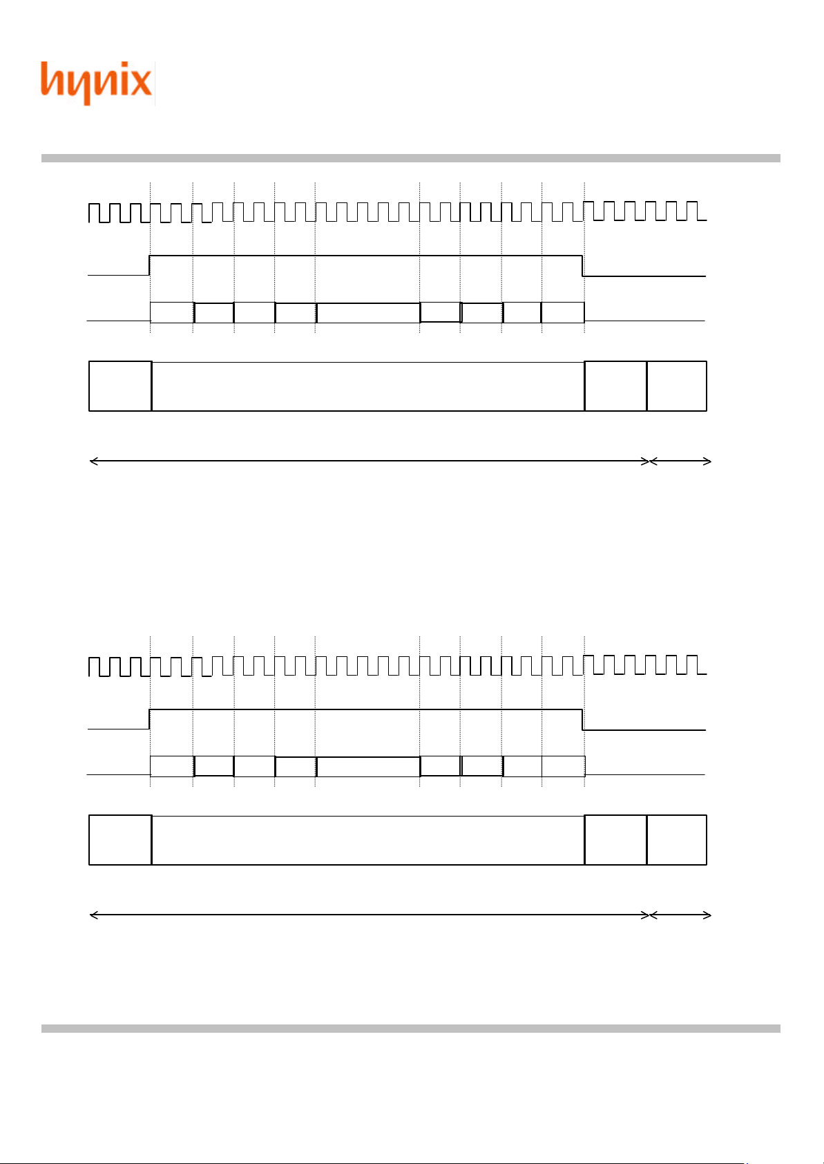
(2) Frame Timing Diagram for Integration Time > (EffectiveWindowHeight * Scale)
Frame timing related registers are programmed to suit for the above condition as follows
RowStartAddress = 6; WindowHeight = 302;
ColumnStartAddress = 6; WindowWidth = 402;
IntegrationTime = 600 [Line Mode];
EffectiveWindowHeight is “302” for (SensorArrayHeight > (RowStartAddress + WindowHeight + 1)),
This document is a general product description and is subject to change without notice. Hy nix Semiconductor does not assume
any responsibility for use of circuits described. NO patent licenses are implied.
DA21000601R_1.0 - 24 - 2001 Hynix System IC SBU
i.e. 314 > (6 + 302 + 1), is met, and Scale is “1” for integration time is line mode. Therefore,
(Integration Time < EffectiveWindowHeight * Scale), i.e. 600 > 302 * 1, is met, and Idle Slot of Line
Mode, i.e. (600 - 302) * 1024 clocks idle slot, is inserted before the next frame initiation.
Page 25
Semiconductor Inc.
Line 301
ENB
Sensor Reset
One Line Time Delay
[417 clocks]
VSYNC
Integration Time *
Line 0
Line 1
Line 2
Line 300
Line 301
VSYNC
Line 0
Line 1
Line 2
Line 300
VSYNC
Line 0
Line 1
Line 2
Line 300
Line 301
VSYNC
System IC SBU
Overall Frames Sequence
Initial Data Setup Time
CMOS IMAGE SENSOR
Frame 0 Frame 1 Frame 2
....
Idle Time
....
Idle Time
....
HV7121B
With 8-bit ADC
Idle Time
MCLK
ENB
VSYNC
Delay
Slots
Deglitch
2 clocks
SensorArrayHeight clocks
[314 clocks]
Scale clocks
[600 * 414 clocks]
(SensorArrayWidth +
HBLANK) clocks
3 clocks
Fig. 5 Initial Data Setup Time after ENB gets active
This document is a general product description and is subject to change without notice. Hy nix Semiconductor does not assume
any responsibility for use of circuits described. NO patent licenses are implied.
DA21000601R_1.0 - 25 - 2001 Hynix System IC SBU
Page 26
Semiconductor Inc.
IMAGE RAW DATA
Line Head
HBLANK
G G B
Line Tail
SensorArrayWidth (828 )
HBLANK(3)
IMAGE RAW DATA
Line Head
HBLANK
R R G
Line Tail
SensorArrayWidth (828 )
HBLANK(3)
System IC SBU
MCLK
HSYNC
DATA
B⋅
HV7121B
CMOS IMAGE SENSOR
With 8-bit ADC
Time
Slot
Clock
Ruler
MCLK
HSYNC
DATA
Blank
12 clocks
Window Width
804 clocks
Fig.6 Even Line Data Timing
G⋅
Blank
12 clocks
3 clocks
Time
Slot
Blank
12 clocks
Window Width
804 clocks
Blank
12 clocks
3 clocks
Clock
Ruler
Fig.7 Odd Line Data Timing
This document is a general product description and is subject to change without notice. Hy nix Semiconductor does not assume
any responsibility for use of circuits described. NO patent licenses are implied.
DA21000601R_1.0 - 26 - 2001 Hynix System IC SBU
Page 27
Semiconductor Inc.
. . . . .
G
Line Tail
IMAGE RAW DATA
Line Head
. . . .
G
IMAGE RAW DATA
VSYNC
Idle Slot
HBLANK
System IC SBU
MCLK
HSYNC
VSYNC
DATA
HV7121B
CMOS IMAGE SENSOR
With 8-bit ADC
Time
Slot
Window Width
≈
804 clocks
Blank
12 clocks
3 clocks
(Integration Time -
EffectiveWindowHei
ght) * 1024
3 clocks
12 clocks
Integration Time > EffectiveWindowHeight * Scale
Fig.8 Frame Transition Timing
Blank
Window Width
804 clocks
≈
This document is a general product description and is subject to change without notice. Hy nix Semiconductor does not assume
any responsibility for use of circuits described. NO patent licenses are implied.
DA21000601R_1.0 - 27 - 2001 Hynix System IC SBU
Page 28
HV7121B
Semiconductor Inc.
System IC SBU
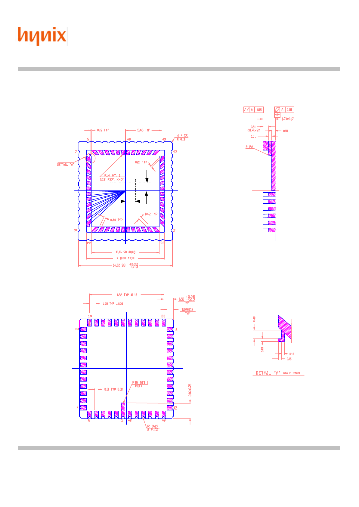
PACKAGE DIMENSION (48 PIN CLCC) UNIT: mm
CMOS IMAGE SENSOR
With 8-bit ADC
* C : Center of Image Area
C
0.53
0.98
This document is a general product description and is subject to change without notice. Hy nix Semiconductor does not assume
any responsibility for use of circuits described. NO patent licenses are implied.
DA21000601R_1.0 - 28 - 2001 Hynix System IC SBU
Page 29

Semiconductor Inc.
System IC SBU
MEMO
HV7121B
CMOS IMAGE SENSOR
With 8-bit ADC
Hynix Semiconductor Inc.
System IC SBU
Headquarter & Factory
San 136-1,Ami-Ri,Bubal-Eub,Ichon-Si,Kyoungki-Do,Korea 467-701
Tel : 82 -2-3459-5573/5577, Fax : 82 -2-3459-5580, E-mail : [email protected]
This document is a general product description and is subject to change without notice. Hy nix Semiconductor does not assume
any responsibility for use of circuits described. NO patent licenses are implied.
DA21000601R_1.0 - 29 - 2001 Hynix System IC SBU
 Loading...