

Page 1
8-Channel Serial to Parallel Converter
with High Voltage Push-Pull Outputs,
POL, Hi-Z, and Short Circuit Detect
HV513
HV513
Features
❑ HVCMOS‚ technology
❑ Operating output voltage of 250V
❑ Low power level shifting from 5V to 250V
❑ Shift register speed 8MHz @ V
❑ 8 latch data outputs
❑ Output polarity and blanking
❑ CMOS compatible inputs
❑ Output short circuit detect
❑ Output high-Z control
DD
=5V
Applications
❏ Piezoelectric transducer driver
❏ Weaving applications
❏ Braille
❏ Printers
❏ MEMs
❏ Displays
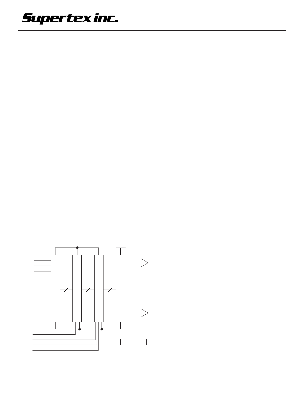
Top Block Diagram
General Description
The HV513 is a low voltage serial to high voltage parallel
converter with 8 high voltage push-pull outputs. This device has
been designed to drive small capacitve loads such as piezoelectric transducers. It can also be used in any application requiring
multiple high voltage outputs, with medium current source and
sink capabilities.
The device consists of an 8-bit shift register, 8 latches, and
control logic to perform the polarity select and blanking of the
outputs. Data is shifted through the shift register on the low to
high transition of the clock. A data output buffer is provided for
cascading devices. Operation of the shift register is not affected
by the /LE, /BL, /POL, or the /HI-Z control inputs. Transfer of data
from the shift register to the latch occurs when the /LE is high.
The data in the latch is stored when /LE is low. A high-Z, /HI-Z,
pin is provided to set all the outputs in a high-Z state.
All outputs have short circuit protection that detects if the outputs
have reached the required output state. If output does not track
the required state, then the /SHORT pin will be low. This output
will pulse low during the output transistion period under normal
operation; see SC Timing Diagram for details.
All outputs will have a break-before-make circuitry to reduce
cross-over current during output state changes.
Note: All logic control inputs have internal 20k-ohm pull-up
resistors.
V
DD
D
IN
CLK
D
OUT
888
8-bit latch
8-bit shift register
LE*
BL*
POL*
Hi-Z*
02/11/02
Supertex Inc. does not recommend the use of its products in life support applications and will not knowingly sell its products for use in such applications unless it receives an adequate "products liability
indemnification insurance agreement." Supertex does not assume responsibility for use of devices described and limits its liability to the replacement of devices determined to be defective due to
workmanship. No responsibility is assumed for possible omissions or inaccuracies. Circuitry and specifications are subject to change without notice. For the latest product specifications, refer to the
Supertex website: http://www.supertex.com. For complete liability information on all Supertex products, refer to the most current databook or to the Legal/Disclaimer page on the Supertex website.
Output control
V
GND
PP
•
•
•
•
•
•
Level translator
HV
OUT
HV
OUT
Short*
1
1
8
Page 2
HV513
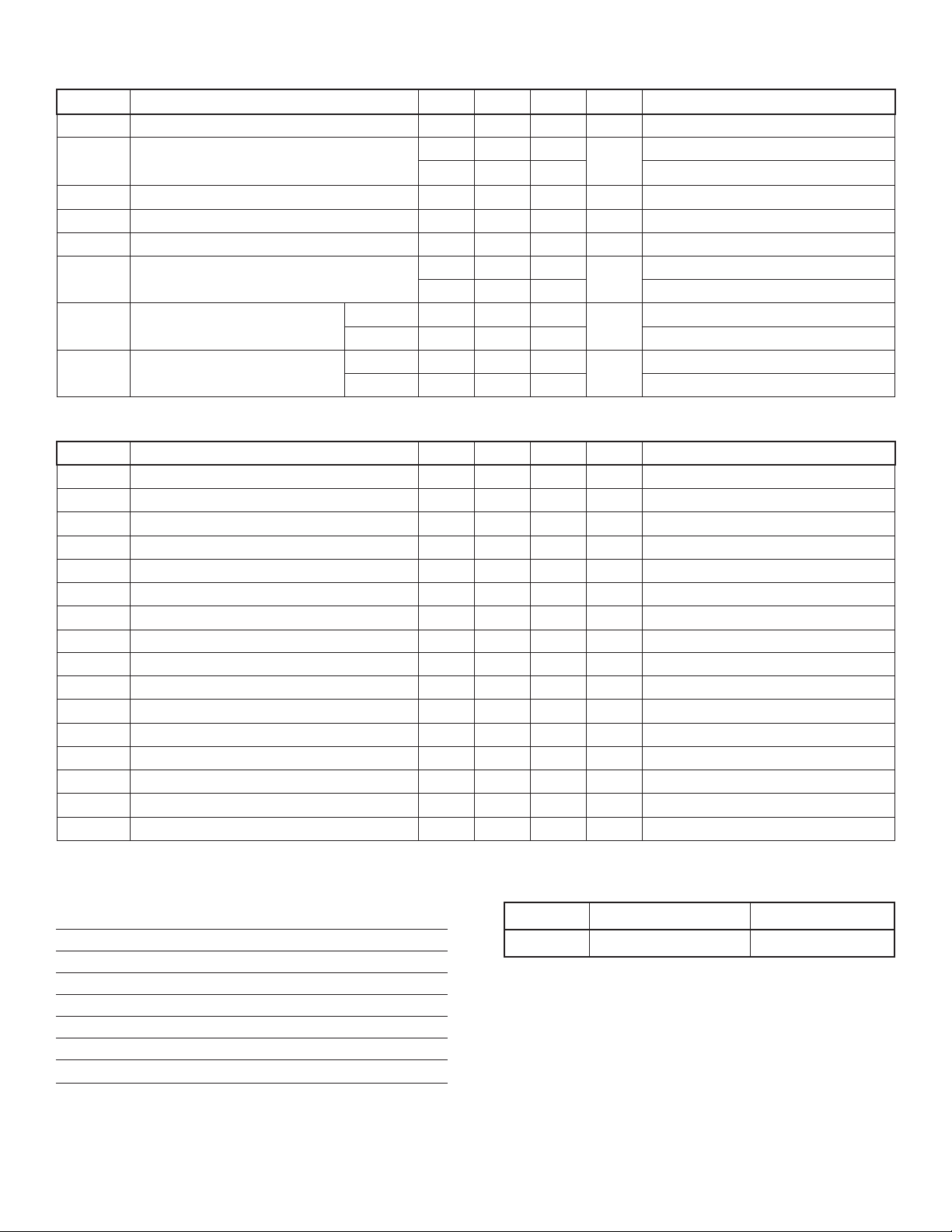
scitsiretcarahClacirtcelECD
lobmySretemaraPniMpyTxaMstinUsnoitidnoC
I
I
I
I
V
V
V
DD
QDD
PP
QPP
I
HI
I
LI
HO
LO
DD
V
PP
tnerrucylppus4Amf
VtnecseiuQ
DD
tnerrucylppus
1.0
0.2VllA
tnerrucylppus001AµVPPf,V052=
VtnecseiuQ
PP
tnerrucylppus001AµV
tnerructupnicigollevel-hgiH01AµVHIV=
tnerructupnicigollevel-woL
H
tuptuolevel-hgiH
tuptuolevel-woL
TUOV
tuoataDV
H
TUOV
tuoataD0.1I
041
V1-I
DD
01-
053-V
06
Am
Aµ
V
V
scitsiretcarahClacirtcelECD
lobmySretemaraPniMpyTxaMstinUsnoitidnoC
ycneuqerfkcolC08zHM
)detimilAOS(ycneuqerfgnihctiwstuptuO003zHCLV,Fn05=
woldnahgihhtdiwkcolC26sn
sesirkcolcerofebemitputesataD51sn
sesirkcolcretfaemitdlohataD03sn
eslupelbanehctalfohtdiW08sn
kcolcfoegdegnisirretfaemityaledEL/53sn
kcolcfoegdegnisirerofebemitputesEL/04sn
VHfoemitllaf/esiR
TUO
0001sµCLV,Fn001=
llaf/esirtratsottuptuorofemityaleD005sn
DotkcolcemityaleD
TUO
DotkcolcemityaleD
TUO
wolothgih011snCLFp51=
hgihotwol011snCLFp51=
stupnicigolllA5sn
noitcetedtiucrictrohstuptuO005sn
raelctiucrictrohstuptuO0001snTROHS/foesirtuptuootraelctrohS
etatsZ-hgihtuptuO005sn
t
t
f
f
t
t
t
t
t
t
ROt,FO
t
t
t
Rt,F
t
t
t
KLC
TUO
W
US
H
ELW
ELD
ELS
FFO/NOd
LHD
HLD
DS
CS
Z-IH
)detonesiwrehtosselnusegatlovylppusgnitareporevO(
KLC
VllA
NIV=DD
V0
=NI
PP
DD
V
V0=
LI
LI
V
PP
TUOD
V
DD
TUOD
I,V002=
Am1.0-=
I,V5.4=
Am1.0=
WOL=*EL,zHM8=
TUO
daolon,zH003=
citatsstuptuo,V042=
srotsiserpu-llup/wstupnirof,V0=
Am02-=
TUOVH
Am02=
TUOVH
)detonesiwrehtosselnusegatlovylppusgnitareporevO(
V002=
PP
V002=
PP
C,TROHS/follaftuptuoottrohS
Fp51=
L
Absolute Maximum Ratings*
Supply Voltage, V
Supply Voltage, V
DD
PP
Logic input levels -0.5V to VDD+0.5V
Ground current 0.3A
High voltage supply current 0.25A
Continuous total power dissipation 750mW
Operating temperature range -40°C to +85°C
Storage temperature range -65°C +150°C
* All voltages are referenced to device ground.
-0.5V to 6V
VDD to 275V
Ordering Information
Device Part Number Package
HV513 HV513WG 24 Lead SOW
2
Page 3
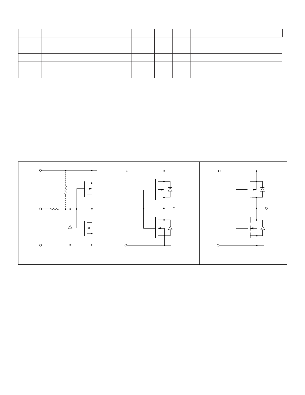
segatloVylppuSgnitarepO
lobmySretemaraPniMpyTxaMstinUsnoitidnoC
V
DD
V
PP
V
HI
V
LI
T
A
Notes:
1. Below minimum VPP the output may not switch.
2. Power-up sequence should be the following:
1. Connect ground.
2. Apply VDD.
3. Set all inputs (Data, CLK, Enable, etc.) to a known state.
4. Apply VPP.
Power-down sequence should be the reverse of the above.
egatlovylppuscigoL5.40.55.5V
ylppusegatlovhgiH03052V 1etoN
egatlovtupnilevel-hgiHV
9.0-V
DD
egatlovtupnilevel-woL09.0V
erutarepmetria-eerfgnitarepO04-58+C°
Input and Output Equivalent Circuits
HV513
DD
V
V
DD
20kΩ
Input
GND
Logic Inputs
*
POL, BL, LE, and HI-Z
V
DD
V
PP
*
GND
Logic Data Output
Data Out
HV
GND
High Voltage Outputs
HV
OUT
3
Page 4
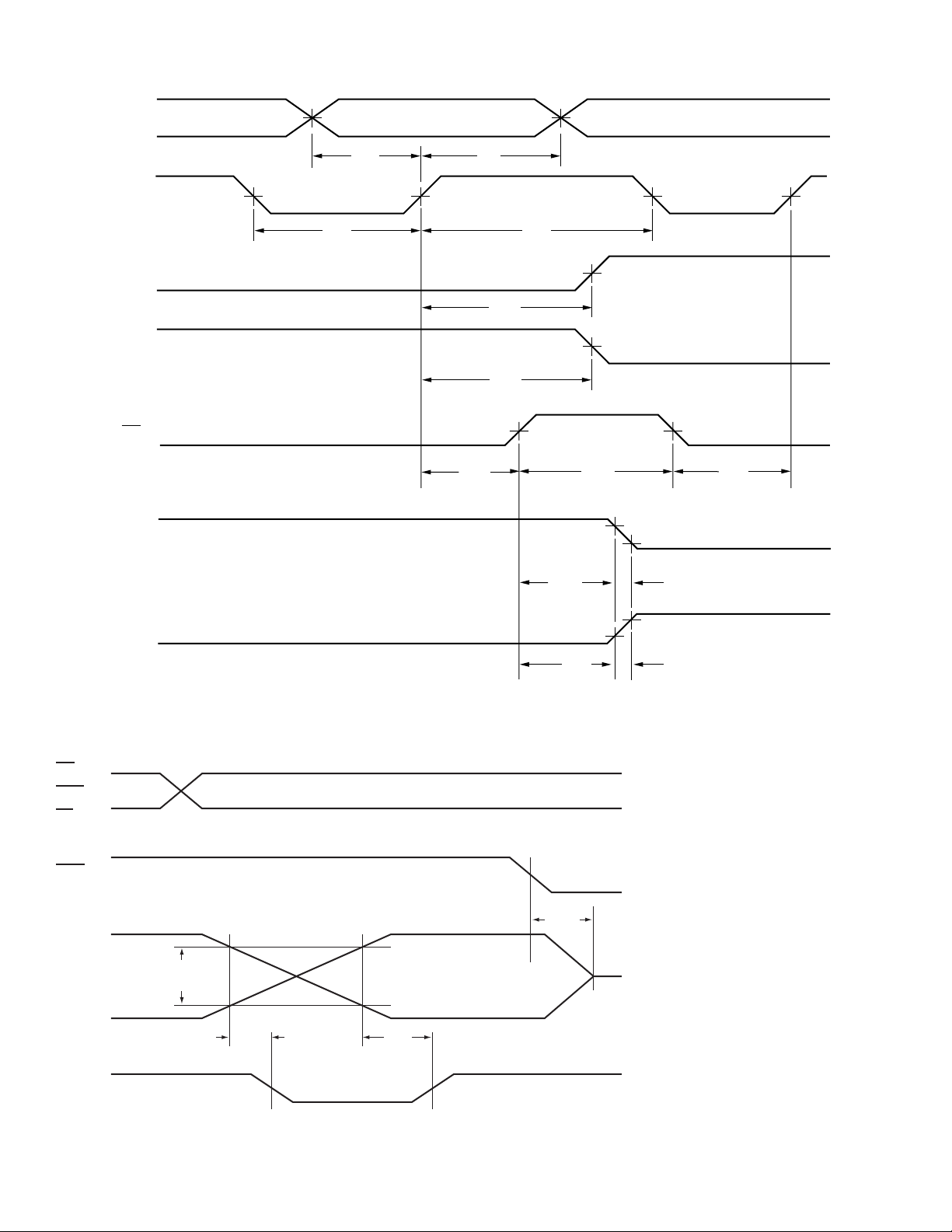
Switching Waveforms
CLK
Data Out
LE
50% 50%
t
WL
HV513
V
IH
Data Valid50% 50%Data Input
V
IL
t
SU
t
H
V
IH
t
50%
WH
50%
V
IL
V
OH
50%
V
OL
V
OH
V
OL
V
IH
V
IL
t
DLE
t
DLH
t
DHL
50%
t
WLE
50%
50%
t
SLE
HV
OUT
w/ S/R LOW
HV
OUT
w/ S/R HIGH
Short Circuit Detect Detail Timing (HV513)
LE
POL
BL
Hi-Z
t
t
HI-Z
d
OFF
t
10%
d
ON
90%
V
V
V
V
V
10%
90%
H
L
IH
IL
OH
t
t
OF
OR
V
OH
V
OL
V
OH
V
OL
HV
OUT
Within
xV of rail
t
SD
t
SC
Short
Detect
If the output is not within 5V to 10V of the desired output state, the SHORT signal goes LOW.
4
V
OL
V
H
V
L
Page 5
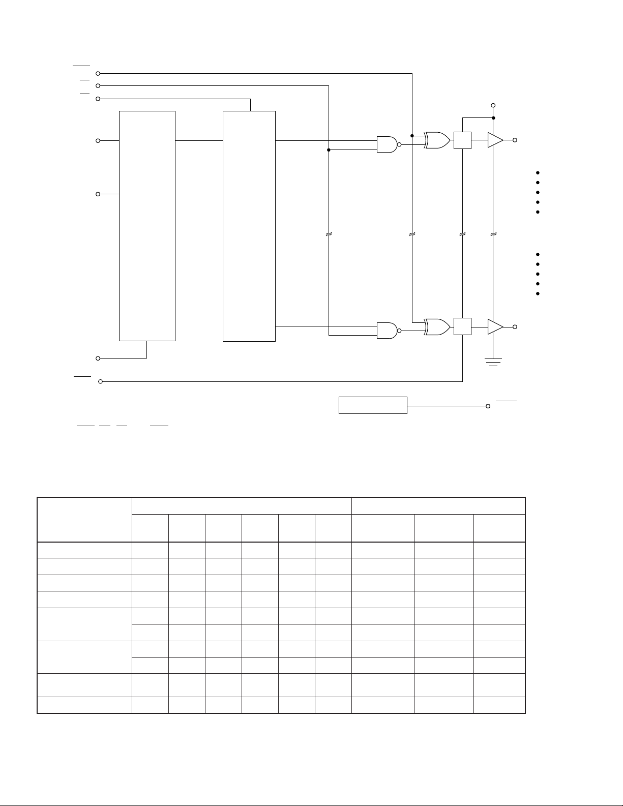
Functional Block Diagram
POL
BL
CLK
8-Bit
Static
Shift
Register
8 Latches
HV
OUT
1
D
OUT
HV
OUT
8
D
IN
LE
HI-Z
Short
POL, BL, LE, and HI-Z have internal 20kΩ pull-up resistors.
Short Detect
6 Additional
Outputs
L/T
L/T
V
PP
HV513
Function Table
nollA XXXLLH *…**H…HH*
ffollA XXXLHH *…**L…LL*
edomtrevnIXXLHLH*…**)b(*…***
R/SdaoLLroHLHHH *…*LroH*…***
NOstuptuO XXXXXH *…***…***
stupnIstuptuO
noitcnuF
ataDKLCEL/LB/LOP/Z-IH/
➔➔➔
XXLHHH *…***…***
sehctalniataDerotS
XXLHLH *…**)b(*…***
edomtnerapsnarT
Z-hgiHstuptuO XXXXXL *…**
L HHHH *…*L*…*L*
H HHHH *…*H*…*H*
➔
geRtfihS
8…21
stuptuOVH
8..21
tuOataD
*
stuptuo
ecnadepmihgiH
*
5
Page 6
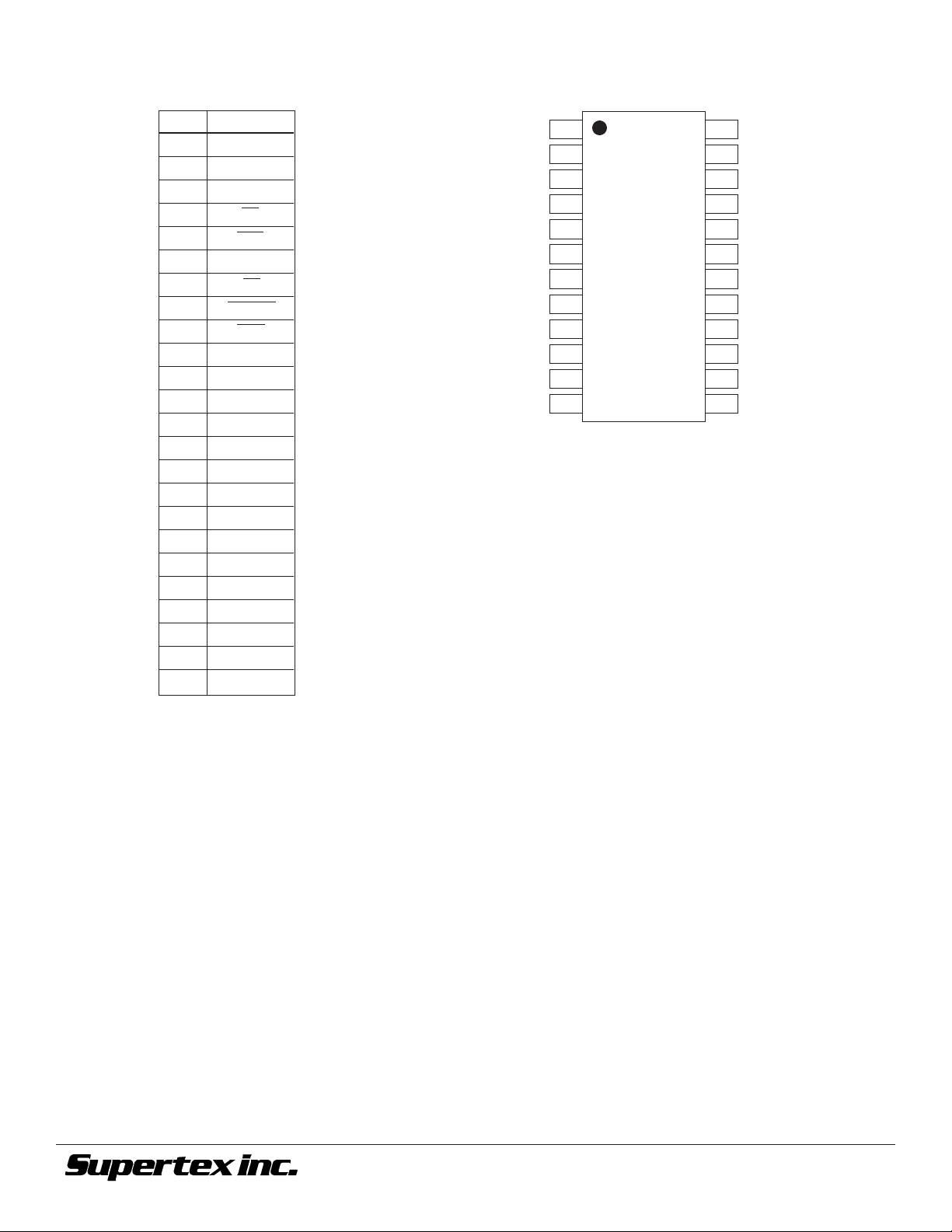
Pin Configuration Package Outline
1
2
3
4
5
6
7
8
9
10
11
12
24
23
22
21
20
19
18
17
16
15
14
13
Pin Function
1 N/C
2V
3D
4BL
5 POL
6 CLK
7LE
8 SHORT
9 HI-Z
10 D
11 LGND
12 N/C
13 HVGND
14 HVGND
15 HV
16 HV
17 HV
18 HV
19 HV
20 HV
21 HV
22 HV
23 V
24 V
DD
OUT
IN
out
out
out
out
out
out
out
out
PP
PP
24-Lead SOW Package (WG)
1
(Wide Body)
2
3
4
5
6
7
8
HV513
©2002 Supertex Inc. All rights reserved. Unauthorized use or reproduction prohibited.
02/11/02
1235 Bordeaux Drive, Sunnyvale, CA 94089
TEL: (408) 744-0100 • FAX: (408) 222-4895
6
www.supertex.com
 Loading...