

Page 1
High Voltage PIN Diode Driver
Ordering Information
Package
Device 20 Pin Ceramic DIP 28 Pin Ceramic J-Lead
HV3922 HV3922C HV3922DJ
HV3922
Features
❏ Processed with HVCMOS® technology
❏ 5V CMOS logic – low power dissipation
❏ DMOS output voltage up to 220V
❏ Low power level shifting – 5V to 220V
❏ Source current 1.7mA
❏ Output fault detection
❏ Latched data output
Absolute Maximum Ratings
Supply Voltage, V
CC
Logic Input Voltage -0.3V to VCC + 0.3V
Supply Voltage V
Supply Voltage V
LL
PP
Max Power Dissipation 0.8W
Junction Temperature +150 °C
Storage Temperature Range -65 °C to +150 °C
Operating Temperature Range -55 °C to +125 °C
Lead Soldering Temperature for 10 Seconds +300 °C
-0.5V to +7.0V
-5.0V
+230V
General Description
The HV3922 is a monolithic high-voltage quad-output driver that
is designed to be used in conjunction with the Supertex
VN2222NC*, a separate N-channel DMOS FET quad array,
whose device characterics are briefly described below. Together,
these devices per-form a 220V push-pull function that is especially suited for driving PIN diodes in applications such as frequency-hopping radios, microwave communication systems and
phased array radar.
Used as a microwave or RF switch, the HV3922 has 4 highvoltage P-channel outputs: PD
controls are Chip Select (CS) and Output Enable (OE) functions.
The HV3922 also has an output fault detection function that
protects the outputs from damage by putting them into a high
impedance state when a short is detected. The HV3922 provides
4 low-voltage outputs—DRV
the gates of the 4 N-channel FETs in the VN2222NC device. See
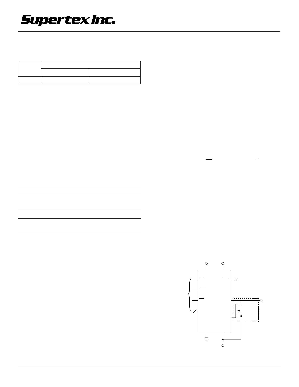
the diagram below for an example of the push-pull output structure that these two devices provide.
For detailed electrical characteristics of the VN2222NC, please
see the data sheet in Chapter 8. Currently, the HV3922 is
available in through-hole and surface-mount ceramic packages
that are suitable for military applications, while the VN2222NC is
offered in ceramic quad and discrete packages (VN2224N2 and
VN2224N3). For commercial product availability, please consult
the factory.
, PD1, PD2 and PD3. Additional
0
, DRV1, DRV2 and DRV3—that drive
0
Push-Pull Configuration
CC
HV39
V
V
LL
HIGH
FAULT
PD0
PD3
DRV0
DRV3
V
220V
Push-Pull
Output
•
•
*VN2222NC
(1 of 4
•
•
LL
FETs)
V
CS
4
ENA
OE
D0 – D3
GND
5V
Digital
Control
* VN2222NC is an N-channel DMOS FET quad array recommended for use in
conjunction with HV39 outputs to form four 220V push-pull outputs. Each of the
four devices has a max R
of 220V.
12/13/01
Supertex Inc. does not recommend the use of its products in life support applications and will not knowingly sell its products for use in such applications unless it receives an adequate "products liability
indemnification insurance agreement." Supertex does not assume responsibility for use of devices described and limits its liability to the replacement of devices determined to be defective due to
workmanship. No responsibility is assumed for possible omissions or inaccuracies. Circuitry and specifications are subject to change without notice. For the latest product specifications, refer to the
Supertex website: http://www.supertex.com. For complete liability information on all Supertex products, refer to the most current databook or to the Legal/Disclaimer page on the Supertex website.
DS(ON)
of 1.25Ω, min I
of 5.0 amps, and BV
D(ON)
DSS
1
Page 2
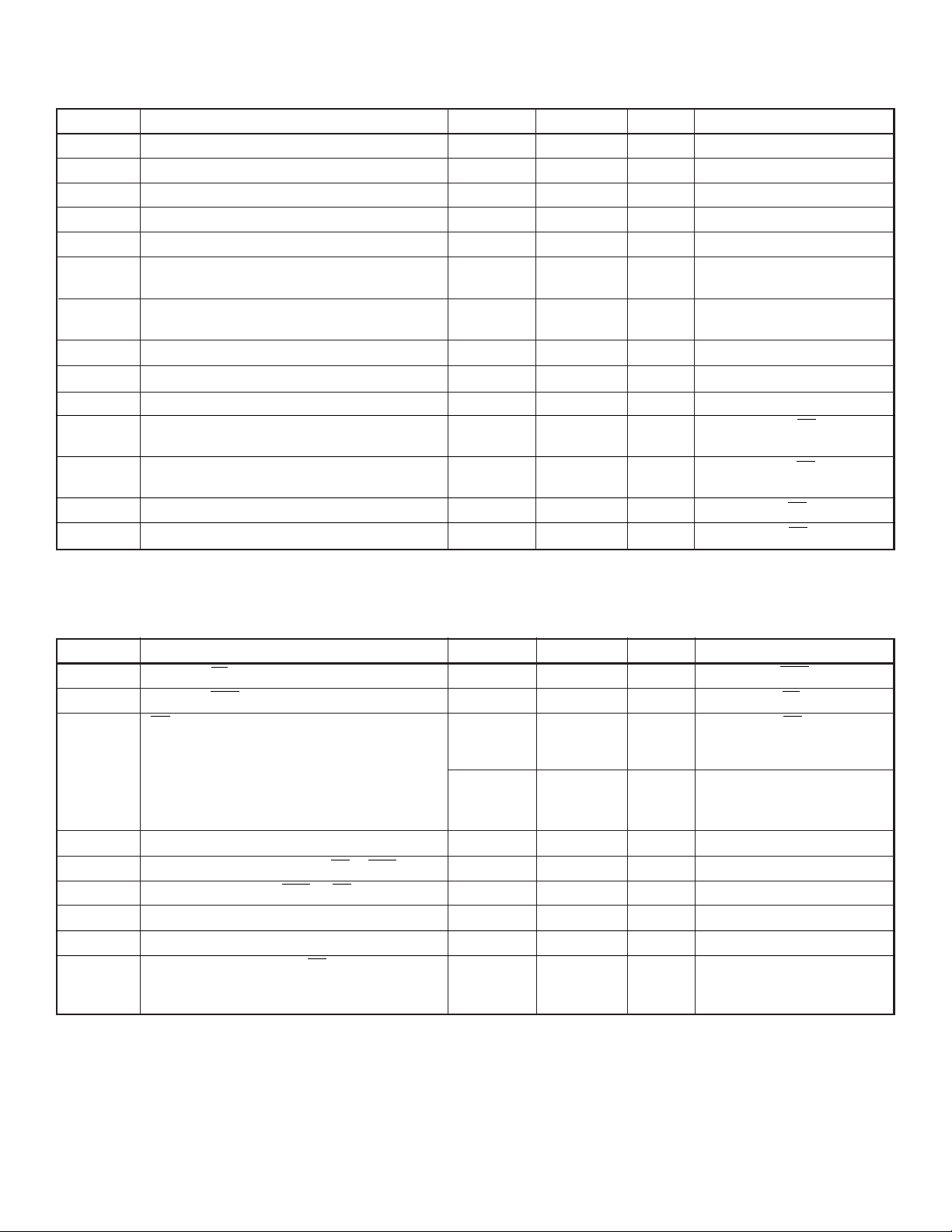
Electrical Characteristics (over recommended operating conditions unless noted)
DC Characteristics
Symbol Parameter Min Max Units Conditions
I
CCQ
I
LLQ
I
PPQ
I
IH
I
IL
V
FH
V
FL
V
DH
V
DH
V
DL
V
TH(min)
V
TH(max)
V
TL(min)
V
TL(max)
Maximum Quiescent VCC Supply Current 1.0 mA V
Maximum Quiescent VLL Supply Current 4.0 mA VLL= -3.5V D
Maximum Quiescent VPP Supply Current 100 µAV
High-level logic current 10 µAH
Low-level logic current 10 µAL
Minimum high-level logic output voltage 4.4 V V
(fault detect)
Maximum low-level logic output voltage 0.1 V V
(fault detect)
Minimum P
Minimum D
Maximum D
Minimum fault threshold for P
high-level output voltage 198 V V
D(N)
high-level output voltage 4 V V
RV(N)
low-output voltage -2.3 V V
RV(N)
output high 0.5 x V
D(N)
PP
VP
fault
Maximum fault threshold for P
output high 0.85 x V
D(N)
PP
VP
fault
Minimum fault threshold for P
Maximum fault threshold for P
output Hi-Z V
D(N)
output Hi-Z V
D(N)
(PDN)
= 0V V P
= 25 V P
(PDN)
= 5.5V All ouputs open
CC
= 220V P
PP
= V
CC
= 0V
= 4.5V, I
CC
= 5.5V, I
CC
= 203V, IOH=1.7mA
PP
= 4.5V, IOH=100µA
CC
= -2.5V, I
LL
= HIGH, OE = V
D(N)
= HIGH, OE = V
D(N)
= Hi-Z, OE = V
D(N)
= Hi-Z, OE = V
D(N)
RV(N)
high or low
D(N)
= 20µA
OH
=-20µA
OL
= -500µA
DL
HV3922
high or low
CC
CC
CC
CC
AC Characteristics (over recommended operating conditions unless noted)
Symbol Parameter Min Max Units Conditions
t
WCS
t
WENA
t
WOE
TT Input transition rise and fall times 0 200 ns VCC= 4.5V
T
SU1
T
SU2
TH Minimum hold time 5 ns VCC= 4.5V
CIN Maximum input capacitance 10 pF Not tested, reference only
TO P
Minimum CS pulse to latch data 100 ns VCC= 4.5V, ENA = 0V
Minimum ENA pulse width to latch data 100 ns VCC= 4.5V, CS = 0V
OE pulse width 10 50 µsVCC= 4.5V, OE = 0V,
= 220V
V
PP
P
LOAD = 20K to GND
D(N)
16 50 µsVPP = 220V,
P
LOAD = 20K and
D(N)
3000pF to GND
Minimum set-up time DN and CS to ENA 150 ns VCC= 4.5V
Minimum set-up time ENA to OE falling edge 150 ns VCC= 4.5V
transition time from OE low to 1 50 µ sVPP = 220V
D(N)
high/low P
P
D(N)
output loaded by
D(N)
20K ohms & 3000pF to GND
2
Page 3
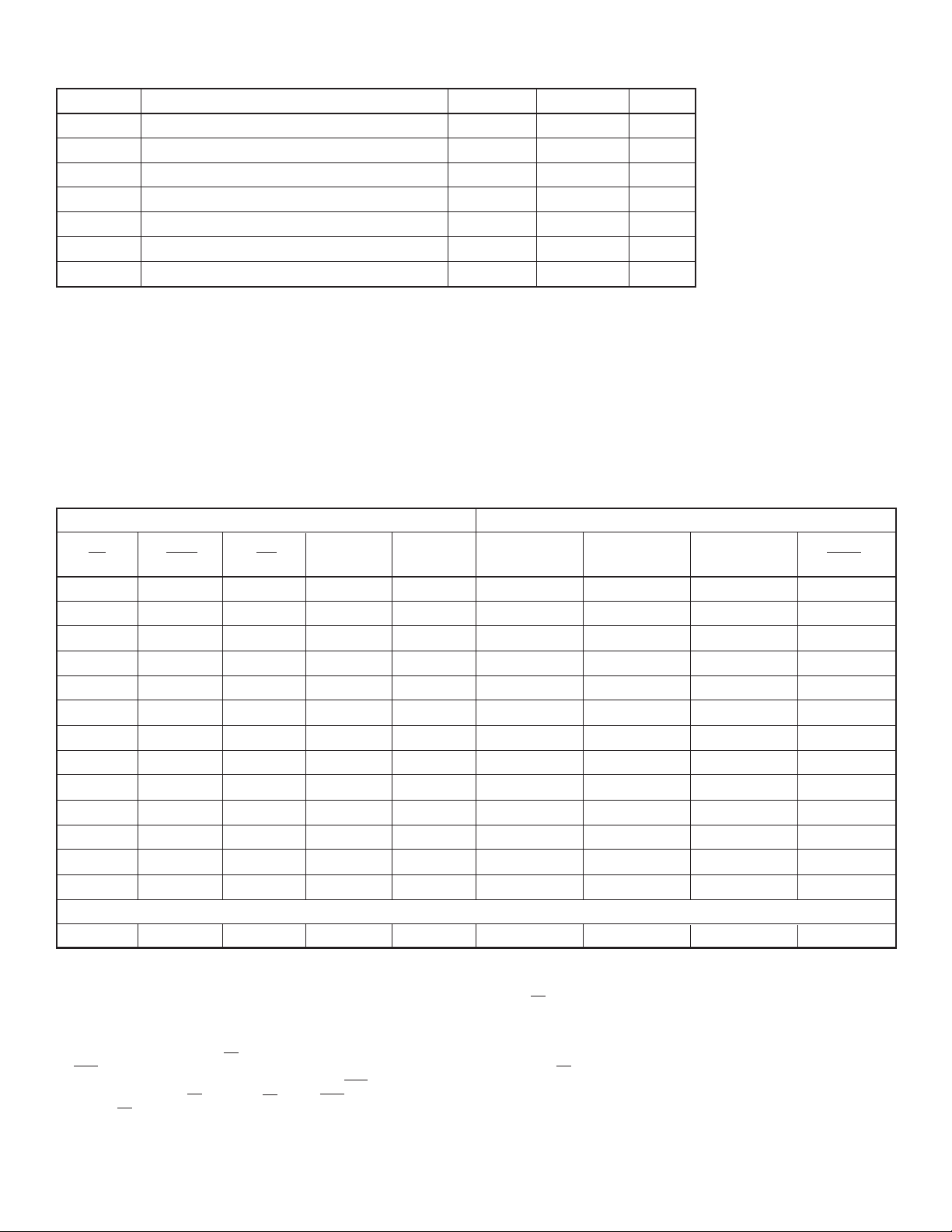
Recommended Operating Conditions
Symbol Parameter Min Max Units
V
CC
V
IN
V
LL
V
PP
IP
D(N)
T
A
CL D
Notes:
rise time (dv/dt) should be less than 50V/µS.
1.V
PP
2.Power-up sequence should be the following:
A) Connect ground;
B) Apply V
C) Apply V
D) Apply V
E) Set all inputs to a known state. Power-down sequence should be the reverse of the above.
Logic Supply Voltage 4.5 5.5 V
DC Logic Input Voltage 0 V
VLL Supply Voltage -3.5 -2.5 V
VPP Supply Voltage 200 220 V
H High-State Continuous P
Source Current 1.7 mA
D(N)
Ambient Operating Temp -55 +125 °C
Load Capacitance 0 0.006 µF
RV(N)
;
CC
;
LL
;
PP
CC
HV3922
V
Function Table
Input Output
Data V
CS ENA OE D
(N)
TH
Level
2
HXHXPass Previous State Previous State Previous State VFH
XHHXPass Previous State Previous State Previous State VFH
LLHHPass Set Previous State Previous State VFH
LLHLPass Reset Previous State Previous State VFH
LLH>L H P/F Set VDH VDL VFH
LLH>L L P/F Reset HI-Z VDH VFH
HXH>L X Previous State
P/F Set VDH VDL VFH
P/F Reset HI-Z VDH VFH
XHH>L X Previous State
Pass Set VDH VDL VFH
Pass Reset HI-Z VDH VFH
XXHXFail — HI-Z VDL VFL
(At Power Up)
XXV
IH
X P/F Set VDH VDL VFH
Internal
Latch Q(N) P
D(N)
D
RV(N)
Fault
Notes:
1. X indicates “Don’t Care” input state (L or H).
2. The output threshold is internally tested for each P
A) P
driving high with output > V
D(N)
OR
B) P
driving Low with output < V
D(N)
The fail condition occurs when OE = H and conditions for “pass” are not satisfied.
3. Fault output = V
condition has been detected for one of the outputs. The Fault output shall remain in the low state, regardless of the state of the output which initiated the fault status, until
the next falling edge of OE. Whenever OE = L, the Fault output is forced to V
time the OE input is set to H.
4. H>L indicates falling edge (H to L).
5. HI-Z indicates no current is sourced to output P
6. P/F indicates “Pass” or “Fail” fault threshold conditions.
indicates a fault has been detected in at least one of the P
FL
TH (MAX)
TH (MIN)
output; the pass condition occurs when OE = H and:
D(N)
, or may occurs if P
, or may occur if P
.
D(N)
driving high and output > V
D(N)
driving low and output < V
D(N)
output loads when OE = H. All other outputs shall function normally when a fault
D(N)
, and the fault latch is reset. If the fault condition persists, the fault response repeats each
FH
TH (MIN)
TH (MAX)
and < V
and < V
TL (MAX)
TL (MIN)
.
.
3
Page 4
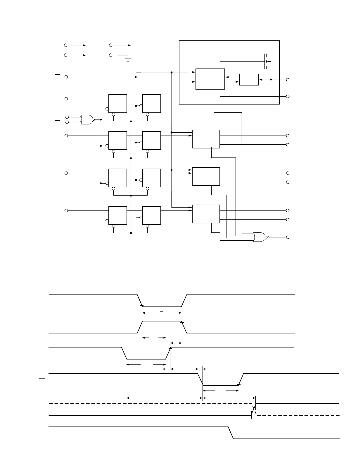
Functional Block Diagram
HV3922
OE
D
O
ENA
CS
D
1
D
2
D
3
V
PP
V
CC
Latch
Set
Latch
Set
Latch
Set
Latch
Set
V
LL
Drive Circuit
V
PP
GND
Gate Control
Circuit
CLK
Set
CLK
Set
CLK
Set
CLK
Set
FF
FF
FF
FF
Q
Q
Drive Circuit
Fault 0
1
Q
Drive Circuit
2
Q
Drive Circuit
3
Q
Q
Q
Q
Voltage
Sense
P
D0
D
RV0
P
D1
D
RV1
P
D2
D
RV2
P
D3
D
RV3
Timing Diagram
DATA LOW
and CS
DATA HIGH
ENA
OE
P
D(N)
10%
Power-Up
Circuit
90%
10% 10%
t
WCS
t
SU1
10%
t
WENA
t
SU2
90%
TT
90%
TH
90%
TT
10%
t
WOE
Fault
10%
t
OH
90%
10%
D
RV(N)
4
Page 5
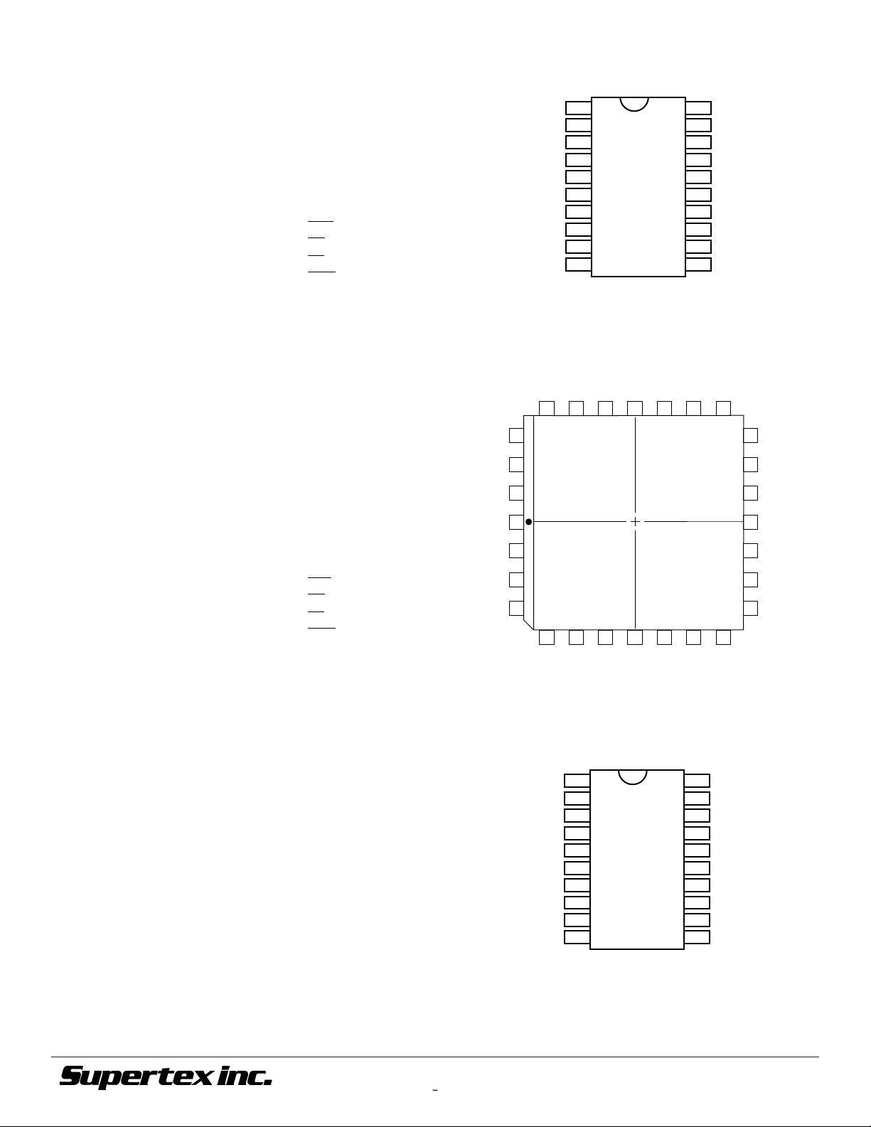
Pin Configurations Package Outline
HV3922
20 Pin, 300 Mil Wide Package
Pin Function
1D
2D
3D
4V
1
2
3
LL
5 GND
6D
RV3
7D
RV2
8P
D3
9P
10 P
D2
D1
28 Pin, J-Lead Package
Pin Function
1D
1
2D
2
3D
3
4 N/C
5V
LL
6 GND
7 N/C
8D
RV3
9D
RV2
10 N/C
11 P
D3
12 N/C
13 P
D2
14 N/C
Pin Function
11 P
12 D
13 D
14 V
15 V
D0
RV1
RV0
PP
CC
16 ENA
17 OE
18 CS
19 Fault
20 D
0
Pin Function
15 P
16 P
D1
D0
17 N/C
18 D
19 D
RV1
RV0
20 N/C
21 V
PP
22 N/C
23 V
CC
24 ENA
25 OE
26 CS
27 Fault
28 D
0
1
2
3
4
5
6
7
8
9
10
20
19
18
17
16
15
14
13
12
11
20 Pin, 300 Mil Wide DIP
HV3922C
24 23 22 21 20
25
26
27
28
1
2
3
4
5
678910
19
18
17
16
15
14
13
12
11
28 Pin J-Lead Package
HV3922DJ
20 Pin, 300 Mil Wide Package
Pin Function
1S
2S
3S
4G
5G
6G
7G
1
2
3
4
8S
9S
10 S
©2001 Supertex Inc. All rights reserved. Unauthorized use or reproduction prohibited.
Pin Function
11 S
12 S
13 N/C
14 D
15 D
16 D
17 D
4
3
2
1
18 N/C
19 S
20 S
1
2
3
4
5
6
7
8
9
10
20
19
18
17
16
15
14
13
12
11
20 Pin, 300 Mil Wide DIP
VN2222NC
12/13/010
1235 Bordeaux Drive, Sunnyvale, CA 94089
5
TEL: (408) 744-0100 • FAX: (408) 222-4895
www.supertex.com
 Loading...