

Page 1
64-Channel Serial To Parallel Converter
With High Voltage Push-Pull Outputs
Ordering Information
Package Options
Recommended 80-Lead 80-Lead
Device Operating Quad Cerpak Quad Plastic Die
VPP Max Gullwing Gullwing
HV3418 180V HV3418DG HV3418PG HV3418X
HV3418
Features
❏ HVCMOS® technology
❏ Output voltages up to 180V
❏ Low power level shifting
❏ Shift register speed: 6MHz @ VDD = 5V
12MHz @ V
❏ Latched data outputs
❏ Output polarity and blanking
❏ CMOS compatible inputs
❏ Forward and reverse shifting options
Absolute Maximum Ratings
Supply voltage, V
Supply voltage, V
Logic input levels -0.5V to V
Ground current
High voltage supply current
Continuous total power dissipation
Operating temperature range Ceramic -55°C to +125°C
Storage temperature range -65°C to +150°C
Notes:
1. All voltages are referenced to GND.
2. Connection to all power and ground pads is required. Duty cycle is limited by
the total power dissipated in the package.
3. For operation above 25°C ambient derate linearly to maximum operating
temperature at 20mW/°C for plastic and at 31.7mW/°C for ceramic.
DD
PP
2
2
= 12V
DD
1
-0.5V to +15V
V
to +200V
DD
DD
3
Ceramic 1900mW
Plastic 1200mW
Plastic -40°C to +85°C
+0.5V
1.5A
1.3A
General Description
The HV34 is a low voltage serial to high voltage parallel converter
with push-pull outputs. This device has been designed for use as
a printer driver for inkjet applications. It can also be used in any
application requiring multiple output high voltage, low current
sourcing and sinking capabilities.
The device consists of a 64-bit shift register, 64 latches, and
control logic to perform the polarity select and blanking of the
outputs. A DIR pin controls the direction of data shift through the
device. With DIR grounded, D
data is shifted from HV
D
is Data-In and D
IOB
HV
1 to HV
OUT
OUT
OUT
IOA
64. Data is shifted through the shift register on
is Data-In and D
IOA
64 to HV
1. When DIR is at logic high,
OUT
is Data-Out: data is then shifted from
the low to high transition of the clock. Data output buffers are
provided for cascading devices. Operation of the shift register is
not affected by the LE (latch enable), BL (blanking), or the POL
(polarity) inputs. Transfer of data from the shift register to the latch
occurs when the LE (latch enable) is high. The data in the latch is
stored during LE transition from high to low.
is Data-Out;
IOB
12/13/01
Supertex Inc. does not recommend the use of its products in life support applications and will not knowingly sell its products for use in such applications unless it receives an adequate "products liability
indemnification insurance agreement." Supertex does not assume responsibility for use of devices described and limits its liability to the replacement of devices determined to be defective due to
workmanship. No responsibility is assumed for possible omissions or inaccuracies. Circuitry and specifications are subject to change without notice. For the latest product specifications, refer to the
Supertex website: http://www.supertex.com. For complete liability information on all Supertex products, refer to the most current databook or to the Legal/Disclaimer page on the Supertex website.
1
Page 2
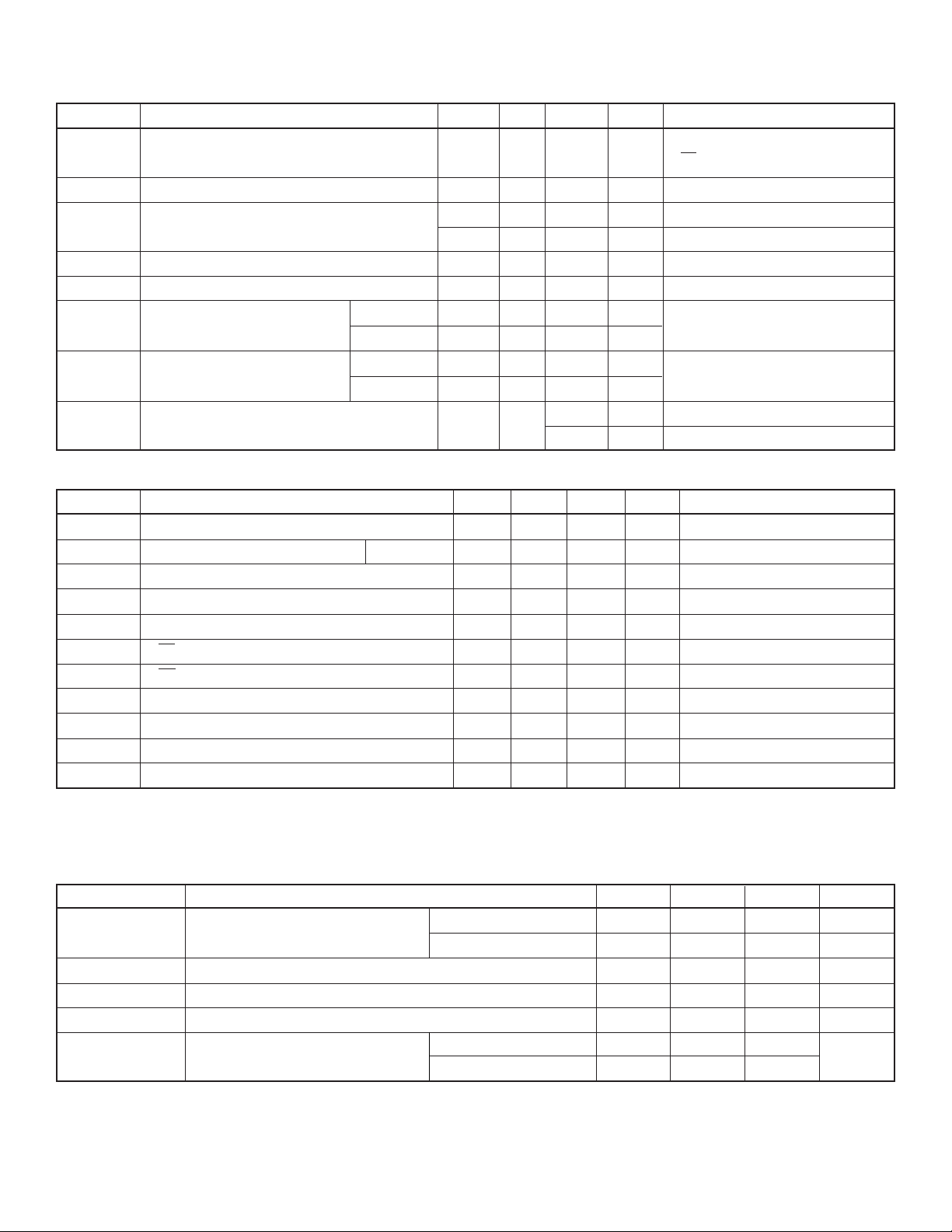
Electrical Characteristics (over recommended operating conditions unless noted)
DC Characteristics
Symbol Parameter Min Typ Max Units Conditions
I
DD
I
DDQ
I
PP
I
IH
I
IL
V
V
V
OH
OL
OC
VDD Supply Current 25 mA f
= 12MHz, f
CLK
LE = LOW
Quiescent VDD Supply Current 200 µA All VIN = 0V or V
High Voltage Supply Current 0.50 mA VPP = 180V All outputs high
0.50 mA V
High-Level Logic Input Current 10 µAVIH = V
= 180V All outputs low
PP
DD
Low-Level Logic Input Current -10 µAVIL = 0V
High-Level Output HV
OUT
Data Out V
Low-Level Output HV
OUT
Data Out 1.0 V ID
HV
Clamp Voltage VPP +1.5 V IOL = +5mA
OUT
155 V VPP = 180V, IHV
-1V V ID
DD
= -100µA
OUT
25 V VPP = 180V, IHV
= +100µA
OUT
-1.5 V I
= -5mA
OL
DATA
DD
OUT
OUT
HV3418
= 12MHz
= -5mA
= +5mA
AC Characteristics
1,2
(For V
= 12V: values in parentheses are for VDD = 5V; VPP = 180V, TA = 25°C)
DD
Symbol Parameter Min Typ Max Units Conditions
f
CLK
t
W
t
SU
t
H
t
WLE
t
DLE
t
SLE
tON, t
OFF
t
DHL
t
DLH
tr, t
f
Notes:
1. Shift register speed can be as low as DC as long as Data Set-up and Hold Time meet the spec.
2. AC Characteristics are guaranteed only under V
Clock Frequency 12(6) MHz
Clock Width High and Low High 40(83) ns
Data Setup Time Before Clock Rises 25(35) ns
Data Hold Time After Clock Rises 10(30) ns
Width of Latch Enable Pulse 62(80) ns
LE Delay Time Rising Edge of Clock 25(35) ns
LE Setup Time Before Rising Edge of Clock 30(40) ns
Time from Latch Enable to HV
OUT
1(1.5) µsC
= 20pF
L
Delay Time Clock to Data High to Low 50(110) ns CL = 20pF
Delay Time Clock to Data Low to High 75(160) ns CL = 20pF
All Logic Inputs 5 ns
= 12V and VDD = 5V.
DD
Recommended Operating Conditions
Symbol Parameter Min Typ Max Units
V
DD
V
PP
V
IH
V
IL
T
A
Notes:
Power-up sequence should be the following:
1. Connect ground. 4. Apply V
2. Apply V
3. Set all inputs (Data, CLK, Enable, etc.) to a known state.
Power-down sequence should be the reverse of the above.
.5.The VPP should not drop below VDD or float during operation.
DD
Logic supply voltage VDD = 5V 4.5 5.0 5.5 V
VDD =12V 10.8 12.0 13.2 V
High voltage supply 60 180 V
High-level input voltage VDD -0.9 V
DD
Low-level input voltage 0 0.9 V
Operating free-air temperature Plastic -40 +85
Ceramic -55 +125
.
PP
V
°C
2
Page 3
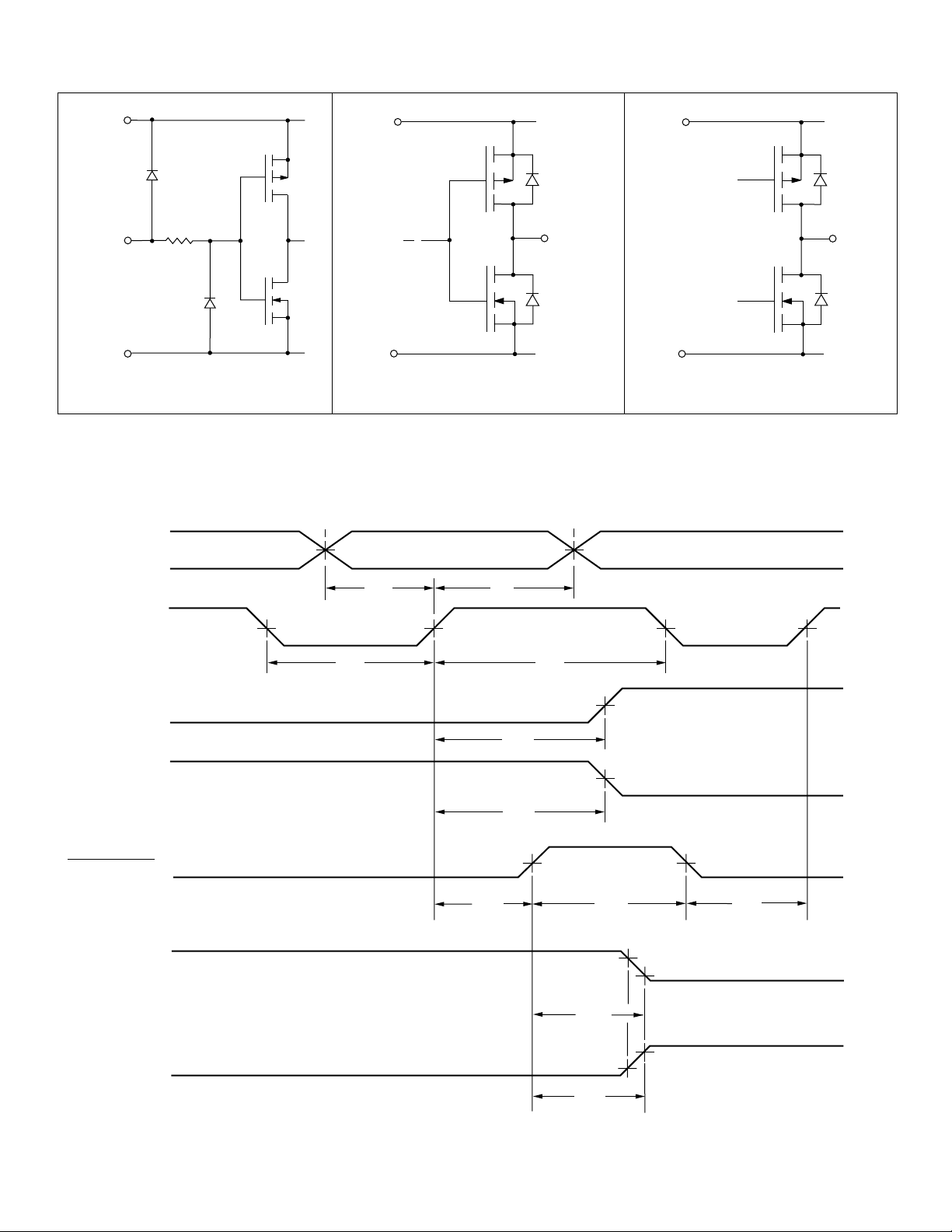
Input and Output Equivalent Circuits
HV3418
V
DD
Input
GND
Logic Inputs
Switching Waveforms
Clock
D
IO/DOI
50% 50% 50%
t
WL
V
GND
t
DD
SU
Logic Data Output
Data Valid50% 50%Data Input
V
PP
Data Out
GND
High Voltage Outputs
t
H
HV
OUT
V
V
V
IH
IL
IH
50%
V
t
WH
IL
V
OH
50%
V
t
DLH
t
50%
DHL
OL
V
OH
V
OL
Latch Enable
HV
OUT
w/ S/R LOW
HV
OUT
w/ S/R HIGH
3
t
DLE
50%
t
OFF
10%
t
ON
t
WLE
90%
10%
90%
50%
t
SLE
V
IH
V
OL
V
OH
V
OL
V
OH
V
OL
Page 4
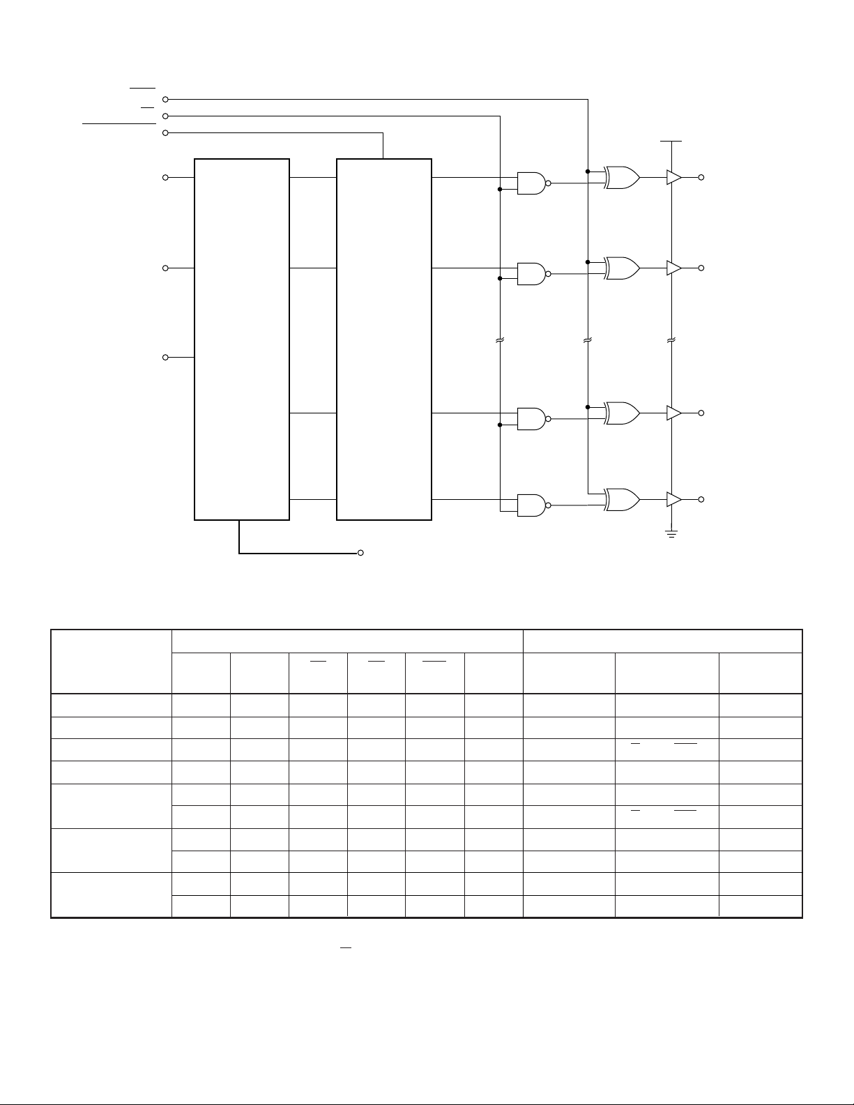
Functional Block Diagram
POL
BL
Latch Enable
HV3418
V
PP
D
IOA
Clock
DIR
64 bit
Static Shift
Register
64 Latches
D
IOB
HV
1
OUT
HV
2
OUT
•
•
•
60 Additional
Outputs
•
•
•
HV
63
OUT
HV
64
OUT
Function Table
Inputs Outputs
Function Shift Reg HV Outputs Data Out
All on X X X L L X * *…*HH…H*
All off X X X L H X * *…*L L…L*
Invert mode X X L H L X * *…** *…**
Load S/R H or L ↑ LHHXH or L *…** *…**
Load/Store Data
in Latches
Transparent
Latch mode
I/O Relation
Notes:
H = high level, L = low level, X = irrelevant, ↑ = low-to-high transition, ↓ = high-to-low transition.
* = dependent on previous stage’s state before the last CLK or last LE high.
Data CLK LE BL POL DIR
12…64 1 2…64 *
XX↓ HHX **…** *…**
XX↓ HLX **…** *…**
L ↑ HHHX L*…*L *…**
H ↑ HHHXH*…*H *…**
D
IOA
D
IOB
↑ XXXLQ
↑ XXXHQ
→ Q
n
→ Q
n
n+1
n-1
—D
—D
IOB
IOA
4
Page 5
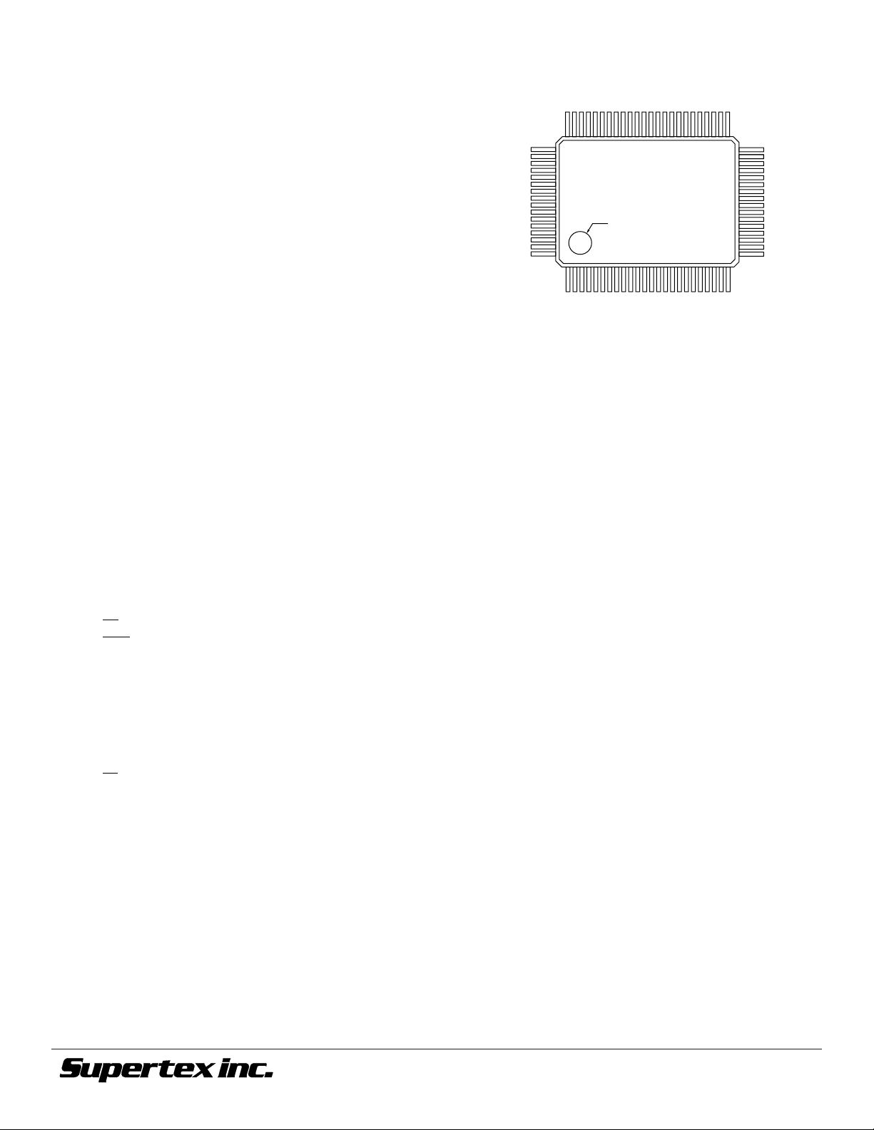
Pin Configurations Package Outline
HV3418
HV34
Pin Function Pin Function
1HV
2HV
3HV
4HV
5HV
6HV
7HV
8HV
9HV
10 HV
11 HV
12 HV
13 HV
14 HV
15 HV
16 HV
17 HV
18 HV
19 HV
20 HV
21 HV
22 HV
23 HV
24 HV
25 V
26 D
41/24 41 HV
OUT
42/23 42 HV
OUT
43/22 43 HV
OUT
44/21 44 HV
OUT
45/20 45 HV
OUT
46/19 46 HV
OUT
47/18 47 HV
OUT
48/17 48 HV
OUT
49/16 49 HV
OUT
50/15 50 HV
OUT
51/14 51 HV
OUT
52/13 52 HV
OUT
53/12 53 HV
OUT
54/11 54 HV
OUT
55/10 55 HV
OUT
56/9 56 HV
OUT
57/8 57 HV
OUT
58/7 58 HV
OUT
59/6 59 HV
OUT
60/5 60 HV
OUT
61/4 61 HV
OUT
62/3 62 HV
OUT
63/2 63 HV
OUT
64/1 64 HV
OUT
PP
IOA
65 HV
66 HV
27 N/C 67 HV
28 N/C 68 HV
29 BL 69 HV
30 POL 70 HV
31 V
DD
71 HV
32 DIR 72 HV
33 LGND 73 HV
34 OGND 74 HV
35 N/C 75 HV
36 N/C 76 HV
37 CLK 77 HV
38 LE 78 HV
39 D
40 V
IOB
PP
79 HV
80 HV
OUT
OUT
OUT
OUT
OUT
OUT
OUT
OUT
OUT
OUT
OUT
OUT
OUT
OUT
OUT
OUT
OUT
OUT
OUT
OUT
OUT
OUT
OUT
OUT
OUT
OUT
OUT
OUT
OUT
OUT
OUT
OUT
OUT
OUT
OUT
OUT
OUT
OUT
OUT
OUT
1/64
2/63
3/62
4/61
5/60
6/59
7/58
8/57
9/56
10/55
11/54
12/53
13/52
14/51
15/50
16/49
17/48
18/47
19/46
20/45
21/44
22/43
23/42
24/41
25/40
26/39
27/38
28/37
29/36
30/35
31/34
32/33
33/32
34/31
35/30
36/29
37/28
38/27
39/26
40/25
64
65
Index
80
1
top view
41
40
25
24
80-pin Gullwing Package
Note:
Pin designation for DIR = H/L
Example: for DIR = H, Pin 1 is HV
for DIR = L, Pin 1 is HV
©2001 Supertex Inc. All rights reserved. Unauthorized use or reproduction prohibited.
OUT
OUT
41
24
12/13/010
1235 Bordeaux Drive, Sunnyvale, CA 94089
TEL: (408) 744-0100 • FAX: (408) 222-4895
5
www.supertex.com
 Loading...