

Page 1
HV301/HV311
HV301
HV311
Demo Kit
Hotswap, Controllers with Circuit Breaker
Available
(Negative Supply Rail)
Features
❑ ±10V to ±90V Operation
❑ Built-in “normally on” turn-on clamp eliminates components
❑ UV/OV Lock Out & Power-on-Reset(POR) for Debouncing
❑ Sense resistor programmed circuit breaker
❑ Programmable circuit breaker holdoff
❑ Inrush control using either: i) servo or ii) feedback cap
❑ Feedback to Ramp pin means no Gate Clamp needed
❑ Application solution for input voltage step (diode “ORing”)
❑ Programmable Auto-Retry (tens of seconds if desired)
❑ Auto-Retry or Latched Operation
❑ Enable through Open Drain interface to UV or OV
❑ Low Power, <0.6mA , <0.4mA Sleep Mode
❑ PWRGD Flag
❑ Small SOIC-8 Package
Applications
❑ -48V Central Office Switching
❑ -24V Cellular and Fixed Wireless Systems
❑ -24V PBX Systems
❑ Line Cards
❑ -48V Powered Ethernet for VoIP
❑ Distributed Power Systems
❑ Power Supply Control
❑ +48V Storage Networks
❑ Electronic Circuit Breaker
General Description
The Supertex HV301 and HV311 Hotswap Controllers provide
control of power supply connection during insertion of cards or
modules into live backplanes. They may be used in systems
where active control is implemented in the negative lead of
supplies ranging from ±10V to ±90V.
During initial power application the gate of the external pass
device is clamped low to suppress contact bounce glitches by a
“normally on” circuit which does not require initialization of the
IC. Thereafter the UV/OV supervisors and power-on-reset work
together to suppress gate turn on until mechanical bounce has
ended. The HV301/311 then control the current inrush limit to a
programmed level using one of two possible methods, i) servo
control or ii) a drain to ramp capacitor. The above methods
eliminate the need for extra hold-off or current limiting components. The devices also include an electronic circuit breaker,
programmed by a sense resistor.
After the load capacitance has fully charged, the HV301/311 will
transition into a low power mode, and enable the open drain
PWRGD. In low power mode the HV301/311 continues to monitor the input voltage and monitor the current level. If a load fault
occurs, the electronic circuit breaker will trip, the pass
element will be turned off, and the PWRGD will return to an
(continued on Page 21)
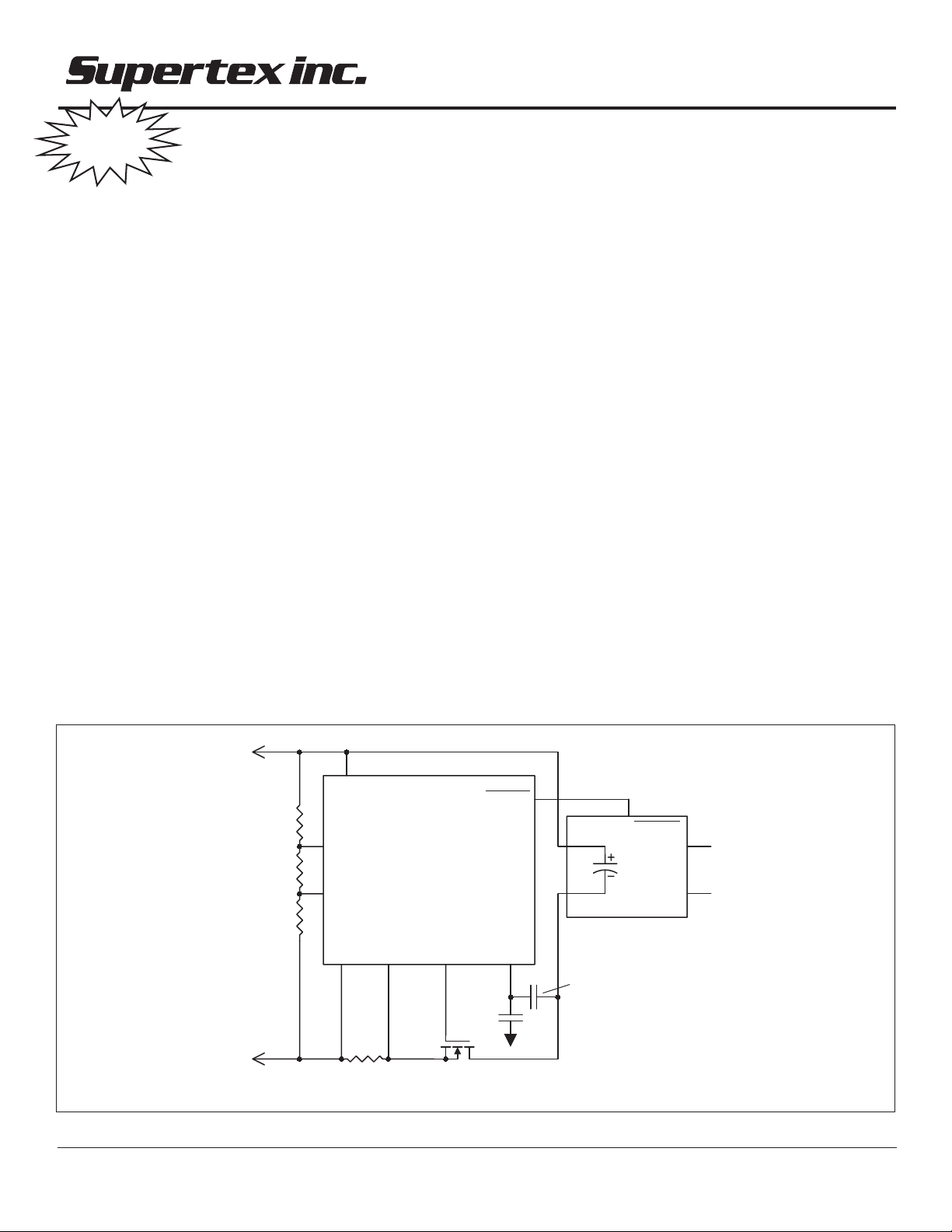
Typical Application Circuit
GND
R1
487kΩ
R2
6.81kΩ
R3
9.76kΩ
-48V
08/26/02
Supertex Inc. does not recommend the use of its products in life support applications and will not knowingly sell its products for use in such applications unless it receives an adequate "products liability
indemnification insurance agreement." Supertex does not assume responsibility for use of devices described and limits its liability to the replacement of devices determined to be defective due to
workmanship. No responsibility is assumed for possible omissions or inaccuracies. Circuitry and specifications are subject to change without notice. For the latest product specifications, refer to the
Supertex website: http://www.supertex.com. For complete liability information on all Supertex products, refer to the most current databook or to the Legal/Disclaimer page on the Supertex website.
8
V
DD
3
UV
2
OV
V
SENSE
EE
54
R4
12.5mΩ
PWRGD / PWRGD
HV301/
HV311
GATE
6
IRF530
Q1
C1
10nF
RAMP
7
C2
-48V
1
ENABLE / ENABLE
Cload
0.75nF
Notes: 1. Undervoltage Shutdown (UV) set to 35V.
+5V
DC/DC
PWM
CONVERTER
2. Overvoltage Shutdown (OV) set to 65V.
3. Current Limit set to -1A.
4. CB set to 8A.
COM
1
Page 2
HV301/HV311
Electrical Characteristics (-10V ≤ V
lobmySretemaraPniMpyTxaMstinUsnoitidnoC
ylppuS
V
EE
I
EE
I
EE
V
HVU
V
LVU
V
YHVU
I
VU
V
HVO
V
LVO
V
YHVO
I
VO
timiLtnerruC
V
V
V
I
I
LC-ESNES
BC-ESNES
ETAG
PUETAG
NWODETAG
VotdecnerefeR(
)nip
DD
egatloVylppuS09-01-V
tnerruCylppuS006007AµV
tnerruCyppuSedoMpeelS004054AµV
lortnoCVUdnaVO
VotdecnerefeR(
)nip
EE
dlohserhThgiHVU62.1V noitisnarThgiHotwoL
dlohserhTwoLVU61.1V noitisnarTwoLothgiH
siseretsyHVU001Vm
tnerruCtupnIVU0.1AnVVUV=
dlohserhThgiHVO62.1V noitisnarThgiHotwoL
dlohserhTwoLVO61.1V noitisnarTwoLothgiH
siseretsyHVO001Vm
tnerruCtupnIVO0.1AnVVOV=
VotdecnerefeR(
)nip
EE
egatloVdlohserhTtimiLtnerruC040506VmVVUV=
egatloVdlohserhTrekaerBtiucriC
tuptuOevirDetaG
VotdecnerefeR(
)nip
EE
egatloVevirDetaGmumixaM5.80121VVVUV=
tnerruCpU-lluPevirDetaG005AµVVUV=
tnerruCnwoD-lluPevirDetaG04AmVVUV=
≤ -90V, -40°C ≤ +85°C unless otherwise noted)
EE
EE
EE
V9.1+
EE
V5.0+
EE
EE
08001021VmVVUV=
EE
EE
EE
V,
EE
VO
gnitimiL=edoM,V84-=
peelS=edoM,V84-=
V,V9.1+
V=
VO
V,V9.1+
V=
VO
V,V9.1+
V=
VO
V,V9.1+
V=
VO
V=
EE
V5.0+
EE
V5.0+
EE
V5.0+
EE
V5.0+
EE
V5.0+
lortnoCgnimiTpmaR
I
PMAR
t
ROP
t
ESIR
t
TIMIL
t
DGRWP
V
PMAR
t
t
t
TIMILTRATS
PIRTBC
OTUA
tnerruCtuptuOniPpmaR01AµV
timiLemiTpUtratS08001021sm
emiTyaleDrekaerBtiucriC0.20.5sµ
tuptuOdooGrewoP
V
V
I
)ih(DGRWP
)ol(DGRWP
)kl(DGRWP
DGRWPotegatloVdeilppA09VevitcanI=DGRWP
egatloVwoLDGRWP5.08.0VI
tnerruCegakaeLmumixaM0.1<01AµV,evitcanI=DGRWP
C:snoitidnoCtseT(
DAOL
C,Fµ001=
PMAR
V,Fn01=
VUV=EE
V,V9.1+
VOV=EE
ESNES
nOnruTetaGotVUmorfemiT0.2sm)1etoNeeS(
VotnOnruTetaGmorfemiT
timiL004sµ
ESNES
edoMtimiLtnerruCfonoitaruD0.5sm
DGRWPottimiLtnerruCmorfemiT0.5sm
edoMtimiLtnerruCniniPpmaRnoegatloV6.3V)2etoNeeS(
emITyaleDtratseRcitamotuA61s
VotdecnerefeR(
)nip
EE
DGRWP
siTEFSOMlanretxE,V5.0+)*035FRI
V0=
DGRWP
scitsiretcarahCcimanyD
t
t
Note 1: This timing depends on the threshold voltage of the external N-Channel MOSFET. The higher its threshold is, the longer this timing.
Note 2: This voltage depends on the characteristics of the external N-Channel MOSFET. Vth = 3V for an IRF530.
* IRF530 is a registered trademark of International Rectifier.
VOLHETAG
VULHETAG
noitisnarTrotarapmoCVO005sn
noitisnarTrotarapmoCVU005sn
tiucricCRlanretxeybdednetxeebyaM
evitcA=DGRWP,Am1=
09=
2
Page 3
HV301/HV311
General Description, cont’d.
inactive state. Thereafter a programmable auto-retry timer will
hold the device off to allow the pass element to cool before
resetting and restarting. The auto-retry can be disabled using a
single resistor if desired.
The HV301/HV311 includes a current mode servo-circuit which
can be used as a return to limit during input voltage steps such
as would be seen in a diode “ORed” situation when power
switches back to regulated supply from battery operation. The
HV301/HV311 allow independent programming of the trigger
level of this phenomenon so that it may be set at a different level
to the current limit level if desired. Under all circumstances the
maximum servo period is limited to 100ms to protect the pass
element.
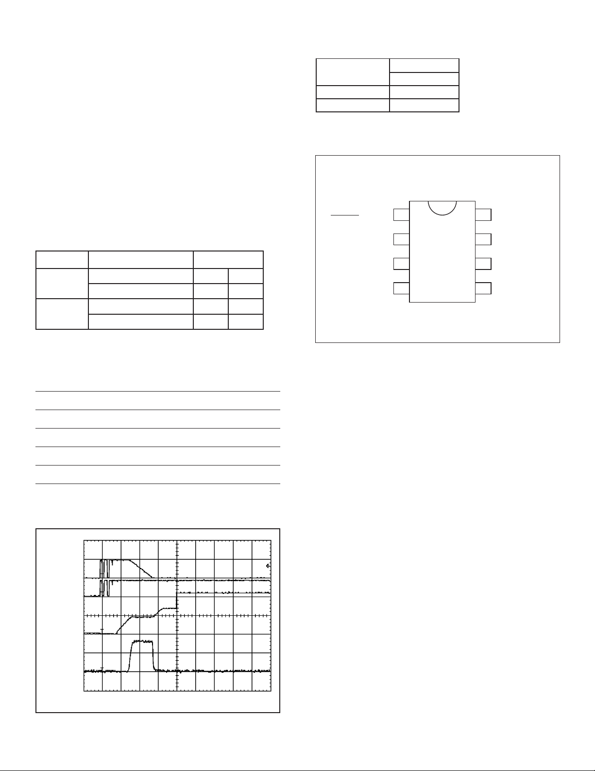
PWRGD Logic
ledoMnoitidnoCDGRWP
103VH
113VH
)ydaeRtoN(EVITCANI0V
)ydaeR(EVITCA1ZIH
)ydaeRtoN(EVITCANI1ZIH
)ydaeR(EVITCA0V
EE
EE
Ordering Information
foetatSevitcA
angiSdooGrewoP l
HGIHGL103VH
WOLGL113VH
snoitpOegakcaP
OSniP8
Pinout
PWRGD (HV301)
PWRGD (HV311)
1
OV
2
UV
3
4
V
EE
8
7
6
5
V
DD
RAMP
GATE
SENSE
Absolute Maximum Ratings
VEE reference to VDD pin +0.3V to -100V
V
referenced to VEE Voltage -0.3V to +100V
PWRGD
VUV and VOV referenced to VEE Voltage -0.3V to +12V
Operating Ambient Temperature -40°C to +85°C
Operating Junction Temperature -40° C to +125°C
Storage Temperature Range -65°C to +150°C
Waveforms
Drain
50V/div
V
IN
50V/div
Gate
5.00V/div
Pin Description
PWRGD – The Power Good Output Pin is held inactive on initial
power application and will go active when the external MOSFET
is fully turned on. This pin may be used as an enable control
when connected directly to a PWM power module.
OV – This OverVoltage (OV) sense pin, when raised above its
high threshold will immediately cause the GATE pin to be pulled
low. The GATE pin will remain low until the voltage on this pin falls
below the low threshold limit, initiating a new start-up cycle.
UV – This UnderVoltage (UV) sense pin, when below its low
threshold limit will immediately cause the GATE pin to be pulled
low. The GATE pin will remain low until the voltage on this pin
rises above the high threshold limit, initiating a new start-up
cycle.
– This pin is the negative terminal of the power supply input
V
EE
to the circuit.
VDD – This pin is the positive terminal of the power supply input
to the circuit.
RAMP – This pin provides a current output so that a timing ramp
voltage is generated when a capacitor is connected.
GATE – This is the Gate Driver Output for the external NChannel MOSFET.
SENSE – The current sense resistor connected from this pin to
VEE Pin programs the circuit breaker trip limit.
I
inrush
500mA/div
5.00ms/div
3
Page 4
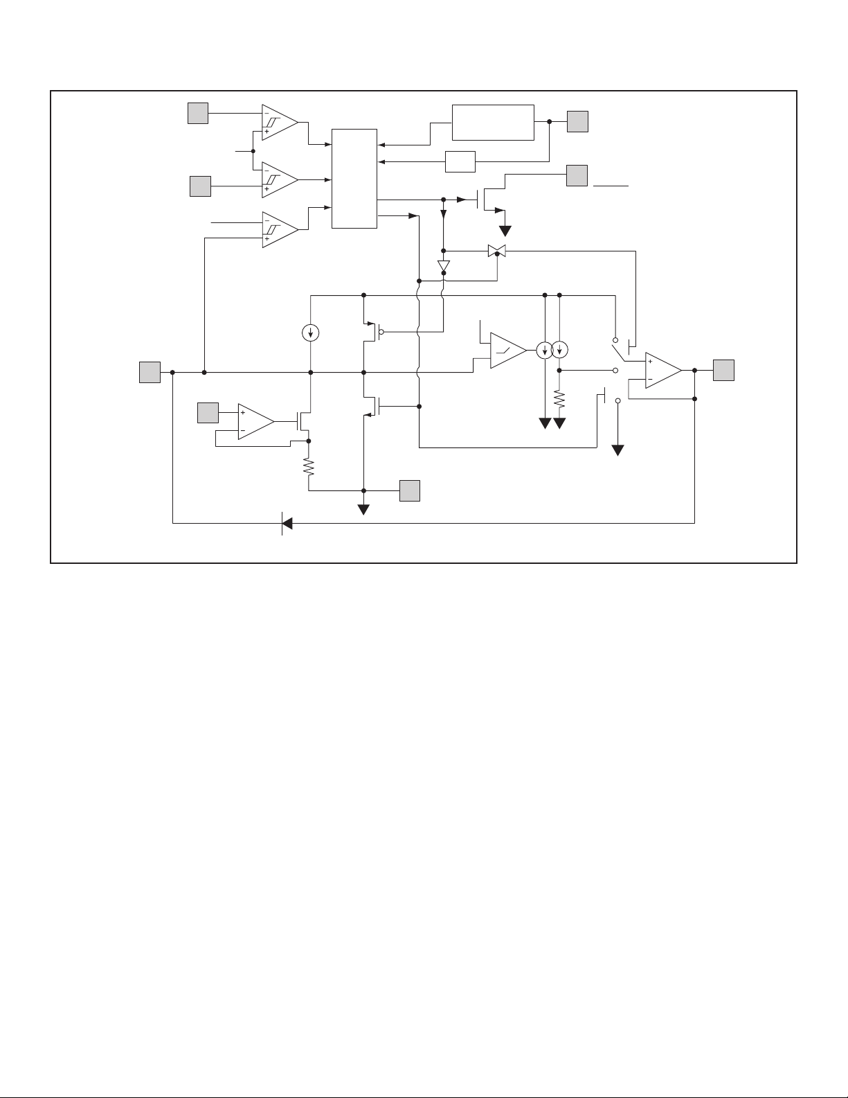
Functional Block Diagram
HV301/HV311
RAMP
UV
OV
~9.8V
SENSE
Vbg
Transconductor
gm
C
C
C
Latch High
Sleep
10µA
Regulator & POR
UVLO
Logic
P
U
L
L
D
H
I
I
S
G
A
H
B
L
E
2V
bg
Transconductor
5k
V
EE
V
DD
1 : 2
V
IN
PWRGD = HV301
PWRGD = HV311
mirror
5k
buffer
GATE
Clamp Mechanism
Functional Description
Insertion into Hot Backplanes
Telecom, data networks and some computer applications require the ability to insert and remove circuit cards from systems
without powering down the entire system. All circuit cards have
some filter capacitance on the power rails, which is especially
true in circuit cards or network terminal equipment utilizing
distributed power systems. The insertion can result in high inrush
currents that can cause damage to connector and circuit cards
and may result in unacceptable disturbances on the system
backplane power rails.
The HV301 and HV311 are designed to facilitate the insertion of
these circuit cards or connection of terminal equipment by
eliminating these inrush currents and powering up these circuits
in a controlled manner after full connector insertion has been
achieved. The HV301 or HV311 is intended to provide this
function on supply rails in the range of ±10 to ±90 Volts.
Description of Operation
During initial power application, a unique proprietary circuit holds
off the external MOSFET, preventing an input glitch while an
internal regulator establishes an internal operating voltage of
approximately 10V. Until the proper internal voltage is achieved
all circuits are held reset, the PWRGD output is inactive and the
gate to source voltage of the external MOSFET is clamped low.
Once the internal under voltage lock out (UVLO) has been
satisfied, the circuit checks the input supply undervoltage (UV)
and overvoltage (OV) sense circuits to ensure that the input
voltage is within programmed limits. These limits are determined
by the selected values of resistors R1, R2 and R3, which form a
voltage divider.
Assuming the above conditions are satisfied and while continuing to hold the PWRGD output inactive and the external MOSFET
GATE voltage low, the current source feeding the RAMP pin is
turned on. The external capacitor connected to it begins to
charge, thus starting an initial time delay determined by the value
of the capacitor. During this time if the OV or UV limits are
exceeded, an immediate reset occurs and the capacitor connected to the RAMP pin is discharged.
When the voltage on the RAMP pin reaches an internally set
threshold voltage, the gate drive circuit begins to turn on the
external MOSFET. In servo mode, once the gate threshold is
reached, the resulting output current generates a voltage drop
on the sense resistor connected between the SENSE and V
pins, causing a decrease in the available current charging the
capacitor on the RAMP pin. This continuous feedback mechanism allows the output current to rise inverse exponentially over
a period of a few hundred microseconds to the sense resistor
programmed current limit set point.
When the voltage drop on the sense resistor reaches 50mV the
RAMP pin current is reduced to zero and the voltage on the
EE
4
Page 5

Functional Description, cont’d.
RRR1 500 2 3 483= −−=kkΩΩ
RAMP pin will be fixed, indicating that the circuit is in current limit
mode. Depending on the value of the load capacitor and the
programmed current limit, charging may continue for some time,
but may not exceed a nominal 100ms preset time limit. Once the
load capacitor has been charged, the output current will drop,
reducing the voltage on the SENSE pin, which in turn will
increase the RAMP pin current, thus causing the voltage on the
capacitor connected to the RAMP pin to continue rising, thereby
providing yet another programmed delay. If due to output overload conditions during startup, PWRGD does not achieve an
active state within 100ms or the circuit breaker is tripped, the
circuit is reset, pulling down the GATE to V
capacitor connected to the RAMP pin, changing PWRGD to an
inactive state. A timeout or circuit breaker fault will initiate an
auto-retry if enabled.
On the other hand, in feedback capacitor mode, a current source
of 10µA from the RAMP pin limits the dv/dt of the feedback
capacitor which, in turn, programs Inrush according to
, discharging the
EE
HV301/HV311
Inrush ~ 10µA•C
accurate formula on page 6.)
When the ramp voltage is within 1.2V of the regulated internal
supply voltage, the controller will force the GATE terminal to a
nominal 10V, the PWRGD pin will change to an active state, the
circuit breaker supervisor is enabled and the circuit will transition
to a low power sleep mode.
When the voltage on the SENSE pin rises to 100mV, indicating
an over current condition, the circuit breaker will trip in less than
5µs. This time may be extended by the addition of external
components.
At any time during the start up cycle or thereafter, crossing the
UV and OV limits (including hysteresis) will cause an immediate
reset of all internal circuitry. When the input supply voltage
returns to a value within the programmed UV and OV limits a new
start up sequence will be initiated.
. (See Programming Inrush and ICB for
load/C2
Design Information
Setting UnderVoltage and OverVoltage Shut Down
The UV and OV pins are connected to comparators with nominal
1.21V thresholds and 100mV of hysteresis (1.21V ± 50mV).
They are used to detect under voltage and over voltage conditions at the input to the circuit. Whenever the OV pin rises above
its high threshold (1.26V) or the UV pin falls below its low
threshold (1.16V) the GATE voltage is immediately pulled low,
the PWRGD pin changes to its inactive state and the external
capacitor connected to the RAMP pin is discharged.
Calculations can be based on either the desired input voltage
operating limits or the input voltage shutdown limits. In the
following equations the shutdown limits are assumed.
The undervoltage and overvoltage shut down thresholds can be
programmed by means of the three resistor divider formed by
R1, R2 and R3. Since the input currents on the UV and OV pins
are negligible the resistor values may be calculated as follows:
RR
+
UV V V
=== ×
OFF UVL
OV V V
=== ×
OFF OVH
Where |
Voltage Shut Down Threshold points.
If we select a divider current of 100µA at a nominal operating
input voltage of 50 Volts then
V
EEUV(off)
116
.
126
.
| and |
()
EEUV off
()
EEOV off
V
| relative to VEE are Under & Over
EEOV(off)
23
RR R
++
123
R
3
++
RR R
123
From the second equation for an OV shut down threshold of 65V
the value of R3 may be calculated.
65 3
R
.
OV
3
R
The closest 1% value is 9.76kΩ.
From the first equation for a UV shut down threshold of 35V the
value of R2 can be calculated.
UV
2
R
The closest 1% value is 6.81kΩ.
Then
The closest 1% value is 487kΩ.
126
==
OFF
.k
126 500
×
=
OFF
=
65
116
==
.
×
116 500
.
35
×
k
Ω
500
Ω
.k
969
=
35 2 3
RR
×+
(
500
k
Ω
k
Ω
− =
..
kk
976 681
Ω
)
ΩΩ
50
RR R123
100
V
500++=µ=
A
kΩ
5
Page 6
HV301/HV311
Design Information, cont’d.
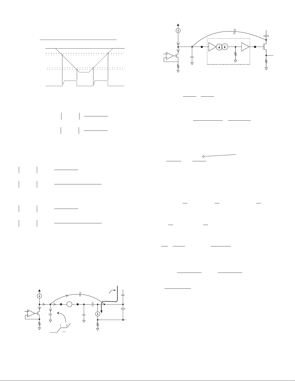
Undervoltage/Overvoltage Operation
GND
UV
OFF
UV
ON
V
IN
OV
ON
OV
OFF
ON
Pass
Transistor
From the calculated resistor values the OV and UV start up
threshold voltages can be calculated as follows:
UV V V
OV V V
Where |
Up Threshold points relative to VEE.
Then
V
EEUV on
V
EEUV on
And
V
EEOV on
V
EEOV on
Therefore, the circuit will start when the input supply voltage is
in the range of 38.29V to 59.85V.
OFF
=== ×
ON UVH
=== ×
ON OVL
()
()
()
()
126
116
.
V
| and |
EEUV(on)
.
=×
126
.
=×
126
.
=×
116
.
=×
116
.
RR R
123
487 6 81 9 76
RR R
123
487 6 81 9 76
()
EEUV on
()
EEOV on
V
| are Under & Over Voltage Start
EEOV(on)
++
RR
+
23
..
++
kkk
ΩΩΩ
..
+
681 976
kk
ΩΩ
++
R
3
..
++
kkk
ΩΩΩ
.
976
RR
+
23
RR R
++
123
R
3
RR R
++
123
k
Ω
.
=
38 29
V
== 59 85.V
10V
C
mirror
2
0.75nF
GATE
Termial
Rsense
V
SENSE
10µA
10µA
Isink
5k
RAMP
terminal
10n=Cramp
1 : 2
Internal Circuitry
1. Choose circuit breaker trip point eg. 8A as follows
100 100
Rsense =
.
Choose inrush level, for example Inrush = 1A
2
3. Calculate Isink
4. Calculate C discharge limit
µµ
= 10 A -Isink = 7.5 A (typical) = iC
mV
I
CB
Inrush*Rsense
==×=µ
2
4a. Adjust for Auto- retry disable, if used
Vt
max
≅
R
⇒ µµ
e.g. iC = 10 A -Isink -1.6 A
disable
e.g.
2
2.5M
mV
==
8
k
5
4V
= 1.6 A
Ω
.
m
12 5
Ω
2
µ
Ω
.
Am
1125
Ω
Ω
k
5
→
Max Vt of a typical
power FET
2.5 A
In this example we assume AutoIn this example we assume Auto- retry is enabled so
ignore 1.6 A, iC = 10 A-Isink = 7.5 A
5. Note: i = C iC = C Inrush = C
Note V is fixed and V is constant during limiting
⇒
µ ∴ µµ
dv
dt
IN RAMP
dv
across C = across C (as they share a
dt
2
22
load
dv
××
dt
load
dv
dt
dv
dt
2
common node and their other terminals are fixed during inrush)
×
iC
2
= ⇒
C
2
Inrush
C
load
Inrush =
iC C
2
C
load
2
48V
Cload
Vsense
Programming Inrush and ICB (Circuit Breaker)
Method 1: Inrush independent of I
10V
0µA
0µA
10n
7.5µA
+ K –
RAMP
dv
on Cramp constant
df
during limiting so no
current flowing into cap
V
SENSE
10µA
7.5µA
2.5µA
5k
GATE
Vgs
C
– +
CB
2
Cgd
+
Cgs
–
inrush
gm(Vgs-Vt)
Rsense=12.5mΩ
+
–
Vin
Cload=100µF
(DRAIN)
Cdb
V
SENSE
by conservation of charge on RAMP Node iC = 7.5 A
Inrush =
75 100
.
µ×
=
AC
75
.
AnF
1
A
load
CC
2
= 750pF = 0.75nF
⇒
C=
2
75
.
AC
µ×
Inrush
µ×
Note that RAMP is protected by AC divider and Gate
is clamped internally.
6
load
µ
2
Page 7
Design Information, cont’d.
HV301/HV311
Programming Inrush and ICB, continued:
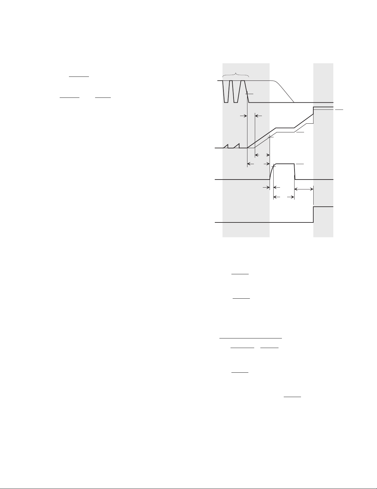
Method 2: Inrush = 1/2 I
1. Choose I =
2. Inrush =
CB
R
100mV
R
50mv
SENSE
SENSE
3. Add compensation components from gate to drain if
necessary to reduce peaking.
(Servo Mode)
CB
, ⇒Ω
e.g. 2A R = 50m
50mV
, e.g.
50m
Ω
SENSE
=1A
Capacitor and/or
compensation resistor
will reduce peaking
Timing (Servo Mode)
contact
bounce
GND
V
IN
V
OUT
V
RAMP
V
GATE
I
IN
activ
PWRGD
inactive
-48V
V
EE
e
t
V
t
POR
RISE
UVL
t
TH
t
START
V
OUT
V
IN
V
GATE
V
RAMP
V
V
GS(th)
90%
V
GATE
t
LIM
GS(lim)
I
LIM
t
PWRGD
i) start with 2nF from gate to source
ii) increase to 10nF if needed
iii) add 1k series resistor from gate to capacitor if needed
Initialization
Limiting
Full On
The timing functions are defined by the following equations:
C
t
START
tV
=
TH
tt t
=+
POR START TH
t
≈
RISE
tV
≈
LIMIT IN
tVV
PWRGD INT
RAMP
=
24
.
I
RAMP
C
GS th
RAMP
()
I
RAMP
C
RAMP
I
RAMP
g
fs
09
.
C
LOAD
I
LIMIT
= −−
()
I
LIMIT
GS
−
()LIMIT
R
SENSE
R
FB
C
RAMP
12
.
I
RAMP
7
Page 8
Design Information, cont’d.
These equations assume that the load is purely capacitive and
the following definitions apply.
C
is the external capacitor connected to the RAMP pin.
RAMP
I
is the output current from the RAMP pin, nominally
RAMP
10µA, when the voltage drop on R
V
is the internally regulated supply voltage and can range
INT
from 8.5V to 12V.
V
is the gate threshold voltage of the external pass
GS(th)
transistor and may be obtained from its datasheet.
V
is the external pass transistor gate-source voltage
GS(
limit
)
required to obtain the limit current. It is dependent on the
pass transistor’s characteristics and may be obtained from
the transfer characteristics on the transistor datasheet.
g
is the transconductance of the external pass transistor
fs
and may be obtained from its datasheet.
R
is the internal feedback resistor and is nominally 5kΩ.
FB
I
is the load current when the voltage drop on the R
LIMIT
resistor is 50mV.
These equations may be used to calculate the minimum value of
C
for the most critical system performance characteristics.
RAMP
For maximum contact bounce duration protection choose a
value for
C
RAMP
t
and use the following equation:
POR
tI
×
POR RAMP
=
V
+24.
GS th
()
resistor is zero.
SENSE
SENSE
HV301/HV311
Start up Overload Protection
Start up must be achieved within a nominal 100ms as indicated
by the PWRGD pin transition to the active state or the circuit will
reset and an automatic restart will initiate. If there is an output
overload or short circuit during start up, the circuit will be in
current limit for the 100ms time limit (in servo mode). In feedback
capacitor mode the circuit breaker will shutdown the pass FET
before 100ms.
Circuit Breaker
The circuit breaker will trip in less than 5µs when the voltage on
the SENSE pin reaches a nominal 100mV. A resistor in series
with the SENSE pin and a capacitor connected between the
SENSE and V
pins may be added to delay the rate of voltage
EE
rise on the SENSE pin, thus permitting a current overshoot and
delaying Circuit Breaker activation.
Automatic Restart
The automatic restart delay time is directly proportional to the
capacitance at the RAMP pin. Automatic restart sequence is
activated whenever the 100ms timeout is reached during start up
or the circuit breaker is tripped.
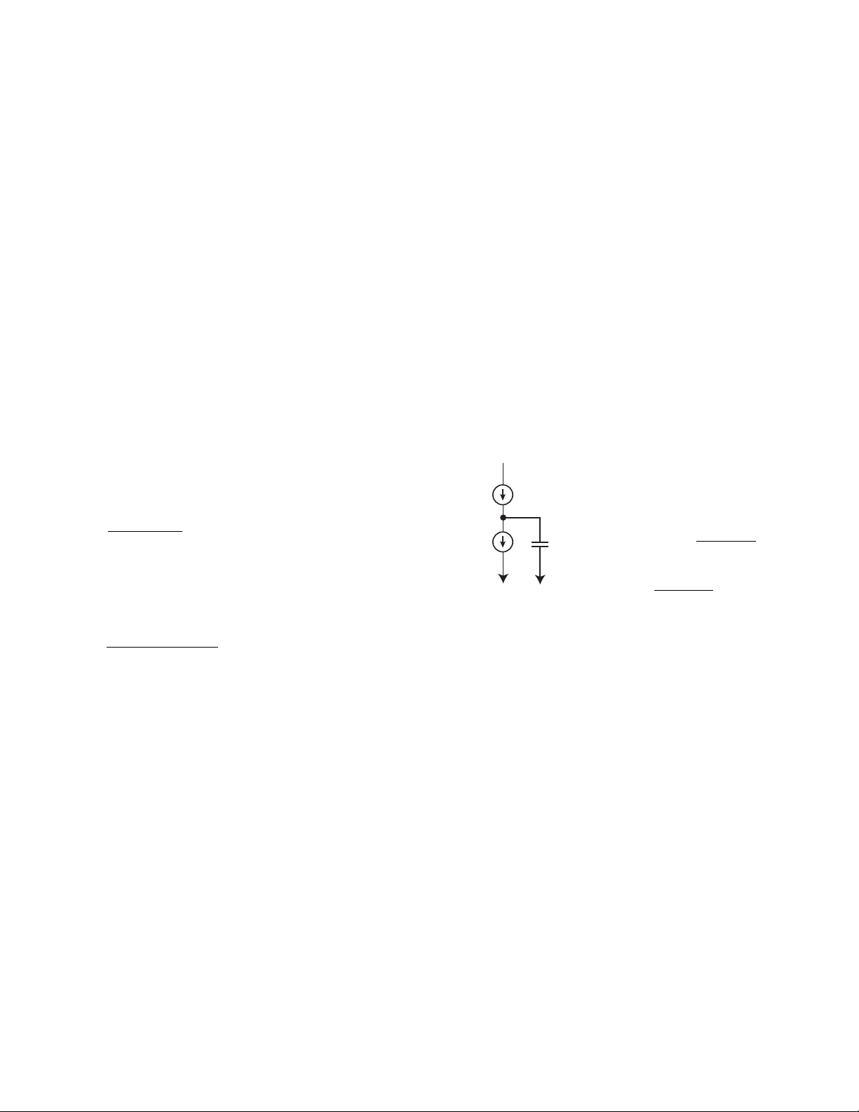
Auto-retry can be approximated as a
555-timer with 2.5µA charge up and
2.5µA
charge down currents through 8V, to
a count of 256. Therefore,
××
2.5µA
T=
C
ramp
AUTORETRY
28256
µ
2.5 A
×
C
ramp
If control of PWRGD active delay is the critical system param-
t
eter, then choose a value for
and use the following
PWRGD
equation:
C
RAMP
tI
=
VV
INT
×
PWRGD RAMP
−−
()
GS
limit
.
12
28256
××
e.g.
2.5 A
µ
Ion =16.4s
×
Due to the 2.5µA max charge current a resistor which draws
more than 2.5µA below 8V will disable the autoretry. Try to
keep this resistor as big as possible, e.g. 2.5MΩ, for most
MOSFETs with max Vt of 4V this will vary the 10µA Ramp
current source by only 4/2.5MΩ=1.6µA.
8
Page 9

Application Information
HV301/HV311
Supported External Pass Devices
The HV301 and HV311 are designed to support N-Channel
MOSFETs and IGBTs.
Selection of External Pass Devices
Since the current limit is likely to be set just slightly higher than
maximum continuous load current in a typical system, the
continuous current rating of the device will have to be at least
equal to the current limit value.
The
R
of the device is likely to be selected based on
DS(ON)
allowable voltage drop after the hot swap action has been
completed. Thus the continuous power dissipation rating of the
device can be determined from the following equation:
PR I
=×
CONT DS ON LIMIT
()
2
The peak power rating may be calculated from the following
equation:
PVI
=×
PEAK IN LIMIT
Given these values an external pass transistor may be selected
from the manufacturers data sheet.
Selection of Current Sense Resistor
The power rating of the sense resistor must be greater than
2
load
×
, where I
IR
is the normal maximum operating load.
load
Paralleling External Pass Transistors
Due to variations in threshold voltages and gain characteristics
between samples of transistors reliable 50% current sharing is
not achievable. Some measure of paralleling may be accomplished by adding resistors in series with the source of each
device; however, it will cause increased voltage drop and power
dissipation.
Paralleling of external Pass devices is not recommended!
If a sufficiently high current rated external pass transistor cannot
be found then increased current capability may be achieved by
connecting independent hotswap circuits in parallel, since they
act as current sources during the load capacitor charging time
when the circuits are in current limit. For this application the
HV301 with active high PWRGD is recommended where the
PWRGD pins of multiple hot swap circuits can be connected in
a wired OR configuration.
Kelvin Connection to Sense Resistor
Physical layout of the printed circuit board is critical for correct
current sensing. Ideally trace routing between the current sense
resistor and the VEE and SENSE pins should be direct and as
short as possible with zero current in the sense traces. The use
of Kelvin connection from SENSE pin and VEE pin to the respective ends of the current sense resistor is recommended.
To
To
SENSE
V
EE
Pin
Pin
To Negative
Terminal of
Power Source
Sense Resistor
To Source
of MOSFET
9
Page 10
HV301/HV311
PWRGD Output
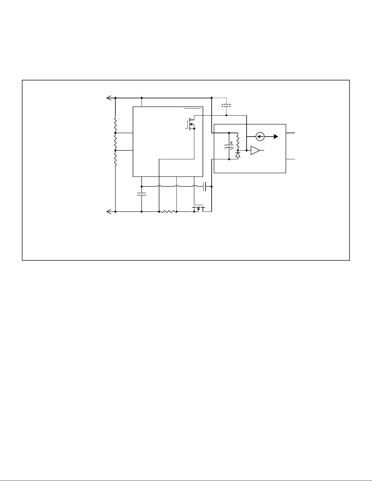
It is critical to have a detailed understanding of the ENABLE input
circuitry of the load (DC/DC PWM Converter) in order to make
the correct choice between the HV301 or HV311.
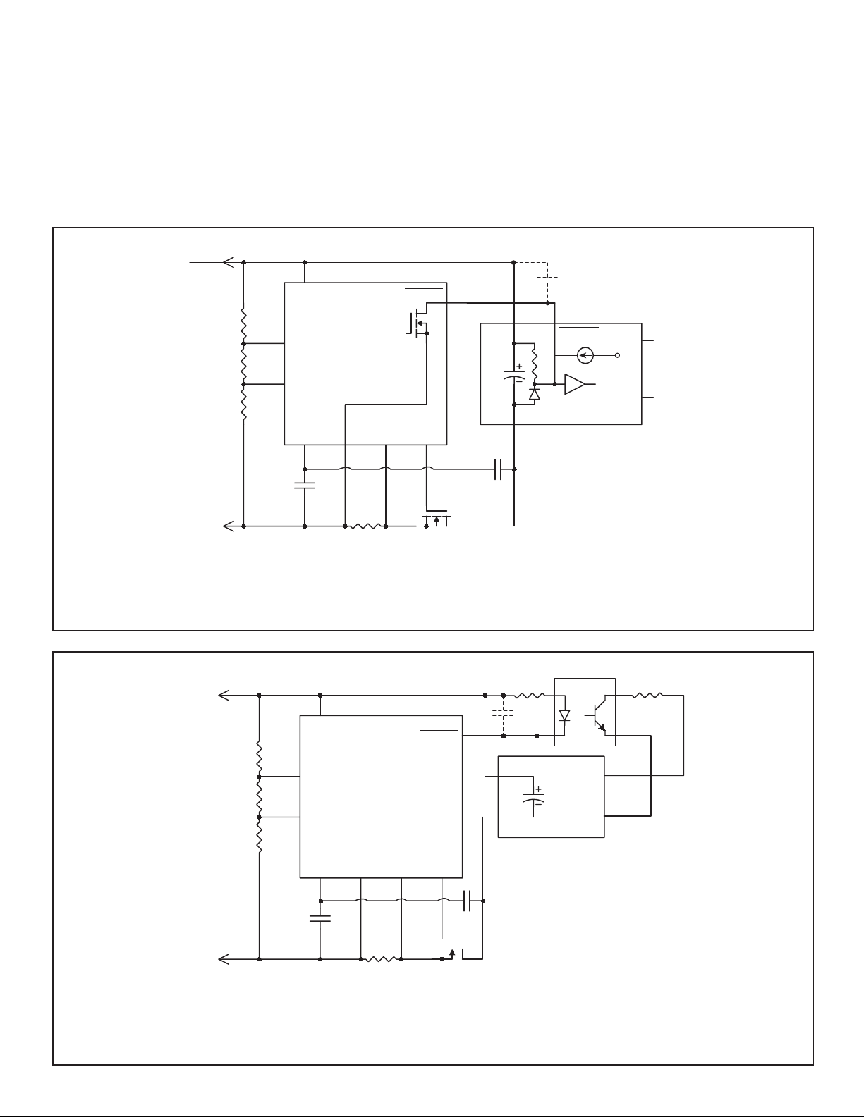
Many DC/DC PWM Converters reference their ENABLE inputs
to the negative input terminal. If the ENABLE input is active LOW
3
2
C1
10nF
UV
OV
8
V
DD
HV311
V
EE
GND
R1
487kΩ
R2
6.81kΩ
R3
9.76kΩ
then the HV311 can be directly connected as shown below
(Application Circuit 1) since the open drain PWRGD output is
in a High-Z state until the external MOSFET is fully turned on and
the potential on the negative input of the converter is essentially
the same as the V
PWRGD
1
+
Cload
-
SENSE GATERAMP
574
6
pin of the HV311.
EE
ENABLE
DC/DC
PWM
CONVERTER
+5V
COM
-48V
R4
12.5mΩ
Note: capacitor may be needed to slow PWRGD dv/dt if
oscillations are observed when V
is close to OV.
IN
Q1
IRF530
Application Circuit 1
10
Page 11
Application Information, cont’d.
HV301/HV311
However, if the DC/DC PWM Converter with the ENABLE input
circuit configuration was active HIGH, then the apparent choice
of the HV301 would result in the creation of a current path
through the protective diode clamp of the ENABLE input and the
PWRGD output MOSFET of the HV301. For this situation the
HV311 should be used as shown below in Application Circuit 2.
GND
R1
487kΩ
R2
6.81kΩ
R3
9.76kΩ
-48V
3
2
C1
10nF
8
V
UV
OV
RAMP
DD
HV311
V
EE
12.5mΩ
SENSE GATE
574
R4
PWRGD
6
Q1
IRF530
In some applications the PWRGD signal is used to activate load
circuitry on the isolated output side of the DC/DC PWM Converter. In this situation an optocoupler is needed to provide the
required isolation as shown below in Application Circuit 3.
1
+
Cload
ENABLE
DC/DC
PWM
-
CONVERTER
+5V
COM
Note: capacitor may be needed to slow PWRGD dv/dt if
oscillations are observed when VIN is close to OV.
GND
R1
487kΩ
R2
6.81kΩ
R3
9.76kΩ
-48V
3
2
C1
10nF
8
V
UV
OV
RAMP
DD
V
EE
12.5mΩ
HV311
SENSE GATE
R4
PWRGD
574 6
Q1
IRF530
Application Circuit 2
Optocoupler
Rload
1
ENABLE
Cload
DC/DC
PWM
CONVERTER
+5V
COM
Note: capacitor may be needed to slow PWRGD dv/dt if
oscillations are observed when VIN is close to OV.
Application Circuit 3
11
Page 12
Application Information, cont’d.
HV301/HV311
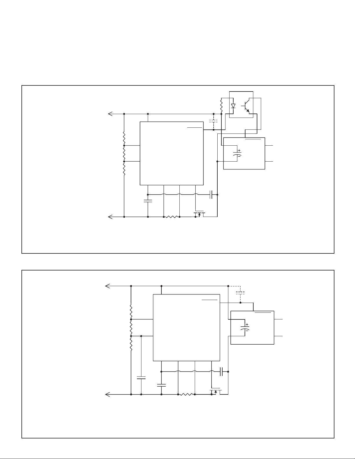
When the details of the load ENABLE circuitry is not known,
using an optocoupler always provides a safe solution
(Application Circuit 4).
GND
R1
487kΩ
R2
6.81kΩ
R3
9.76kΩ
-48V
3
2
C1
10nF
8
V
UV
OV
RAMP
DD
V
EE
Filtering Voltage Spikes on Input Supply
In some systems over voltage spikes of very short duration may
exist. For these systems a small capacitor may be added from
the OV pin to the V
Circuit 5).
PWRGD / PWRGD
HV311
SENSE GATE
574 6
R4
60mΩ
IRF530
Q1
pin to filter the voltage spikes (Application
EE
Optocoupler
1
ENABLE / ENABLE
Cload
DC/DC
PWM
CONVERTER
+5V
COM
Note: capacitor may be needed to slow PWRGD dv/dt if
oscillations are observed when VIN is close to OV.
C2
8
V
3
UV
2
OV
RAMP
GND
R1
487kΩ
R2
6.81kΩ
R3
9.76kΩ
-48V
DD
C1
10nF
HV301/
HV311
V
EE
12.5mΩ
PWRGD / PWRGD
SENSE GATE
574
6
R4
IRF530
Q1
1
ENABLE / ENABLE
Cload
Application Circuit 4
+5V
DC/DC
PWM
CONVERTER
COM
Note: capacitor may be needed to slow PWRGD dv/dt if
oscillations are observed when VIN is close to OV.
Application Circuit 5
12
Page 13
Application Information, cont’d.
HV301/HV311
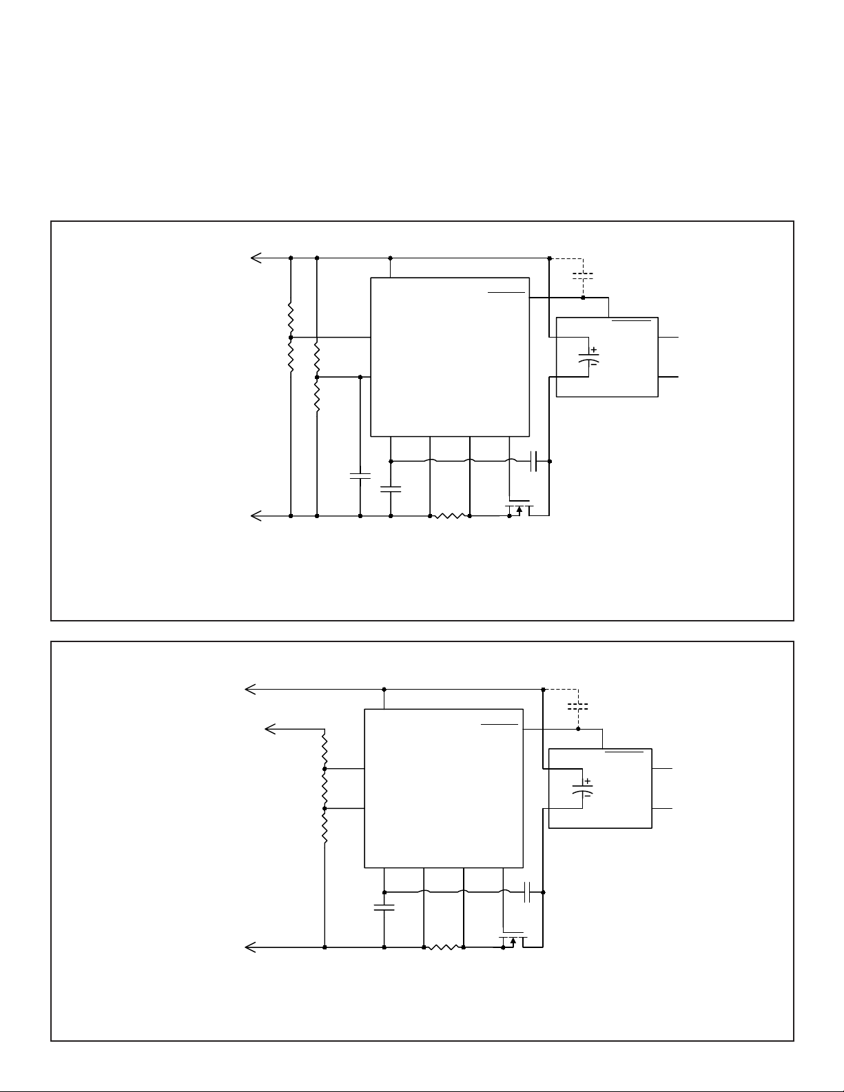
Unfortunately this will also cause some delay in responding to
UV conditions. If this UV delay is not acceptable, then separate
resistor dividers can be provided for OV and UV with a capacitor
connected from OV pin to the V
pin (Application Circuit 6).
EE
GND
R1
475kΩ
R2
16.2kΩ
-48V
R3
511kΩ
R4
10kΩ
C2
3
2
8
V
UV
OV
RAMP
DD
C1
10nF
HV311
V
EE
R5
12.5mΩ
Using Short Connector Pin
In some systems short connector pins are used to guarantee that
the power pins are fully mated before the hotswap control circuit
is enabled. For these systems the positive (V
) end of the R1,
DD
R2, and R3 resistor divider should be connected to the short pin
(Application Circuit 7).
PWRGD / PWRGD
SENSE GATE
574
6
Q1
IRF530
1
ENABLE / ENABLE
Cload
DC/DC
PWM
CONVERTER
+5V
COM
Note: capacitor may be needed to slow PWRGD dv/dt if
oscillations are observed when V
is close to OV.
IN
Long
Pin
GND
-48V
GND
Short
Pin
487kΩ
6.81kΩ
9.76kΩ
Long
Pin
R2
R3
R1
3
2
C1
10nF
8
V
UV
OV
RAMP
DD
PWRGD / PWRGD
HV301/
HV311
V
SENSE GATE
EE
574
R4
12.5mΩ
6
1
Q1
IRF530
Application Circuit 6
ENABLE / ENABLE
Cload
DC/DC
PWM
CONVERTER
+5V
COM
Note: capacitor may be needed to slow PWRGD dv/dt if
oscillations are observed when VIN is close to OV.
Application Circuit 7
13
Page 14
Application Information, cont’d.
HV301/HV311
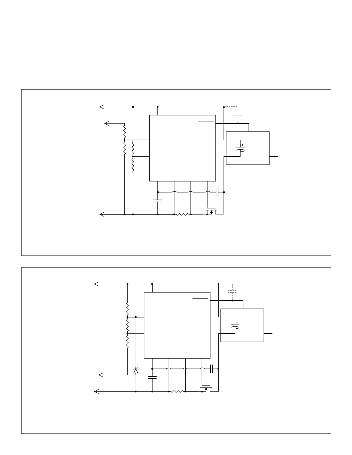
If separate resistor dividers are used for OV and UV, then only
the positive (V
) end of the UV resistor divider should be
DD
connected to the short pin (Application Circuit 8).
If a system requires the use of a short connector pin on the
negative supply lead to guarantee that the power pins are fully
Long
Pin
GND
GND
-48V
475K
16.2K
Long
Pin
Short
Pin
R1
R2
R3
511K
R4
10K
3
2
8
V
UV
OV
RAMP
DD
mated before the hotswap control circuit is enabled and a single
resistor divider string (R1, R2 and R3) is used, then a 6.2V to 10V
zener diode must be connected from the UV pin to the V
as seen below in Application Circuit 9.
PWRGD / PWRGD
HV311
VEESENSE GATE
574
C1
10nF
R5
12.5mΩ
6
Q1
IRF530
1
ENABLE / ENABLE
Cload
DC/DC
PWM
CONVERTER
+5V
COM
EE
pin,
Note: capacitor may be needed to slow PWRGD dv/dt if
oscillations are observed when VIN is close to OV.
Long
Pin
3
2
6.2V
8
V
UV
OV
RAMP
DD
C1
10nF
GND
-48V
-48V
R1
487kΩ
R2
6.81kΩ
R3
9.76kΩ
Short
Pin
Long
Pin
PWRGD / PWRGD
HV311
V
SENSE GATE
EE
5764
R4
12.5mΩ
Q1
IRF530
1
ENABLE / ENABLE
Cload
Application Circuit 8
DC/DC
PWM
CONVERTER
+5V
COM
Note: capacitor may be needed to slow PWRGD dv/dt if
oscillations are observed when VIN is close to OV.
Application Circuit 9
14
Page 15
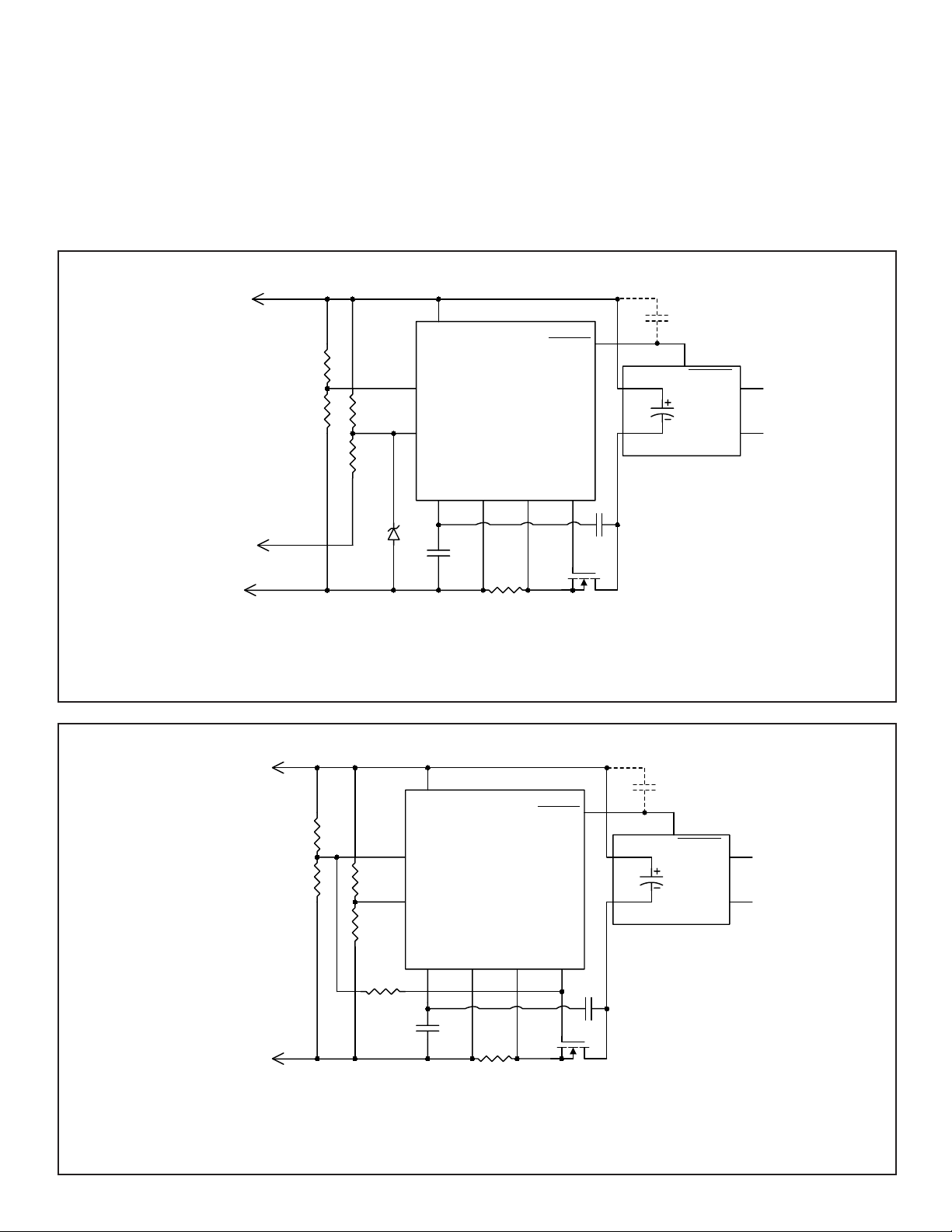
Application Information, cont’d.
HV301/HV311
If a system requires the use of a short connector pin on the
negative supply lead to guarantee that the power pins are fully
mated before the hotswap control circuit is enabled and uses
separate resistor dividers for UV and OV, then a 6.2V to 10V
zener diode must be connected from the OV pin to the V
pin and
EE
only the OV divider should be connected to the short pin
(Application Circuit 10).
Long
Pin
GND
-48V
-48V
R1
475kΩ
R2
16.2kΩ
Short
Pin
Long
Pin
R3
511kΩ
R4
10kΩ
3
2
6.2V
8
V
UV
OV
RAMP
DD
C1
10nF
V
EE
12.5mΩ
Increasing Under Voltage Hysteresis
If the internally fixed under voltage hysteresis is insufficient for a
particular system application, then it may be increased by using
separate resistor dividers for OV and UV and providing a resistor
feedback path from the GATE pin to the UV pin (Application
Circuit 11).
PWRGD / PWRGD
HV301/
HV311
SENSE GATE
574
R5
6
Q1
IRF530
1
ENABLE / ENABLE
Cload
DC/DC
PWM
CONVERTER
+5V
COM
Note: capacitor may be needed to slow PWRGD dv/dt if
oscillations are observed when VIN is close to OV.
GND
R1
475kΩ
R2
16.2kΩ
-48V
R3
511kΩ
R4
10kΩ
R6
8
V
DD
3
UV
2
OV
RAMP
C1
10nF
V
EE
12.5mΩ
PWRGD / PWRGD
HV301/
HV311
SENSE GATE
6
574
R5
IRF530
Q1
1
ENABLE / ENABLE
Cload
Application Circuit 10
+5V
DC/DC
PWM
CONVERTER
COM
Note: capacitor may be needed to slow PWRGD dv/dt if
oscillations are observed when V
is close to OV.
IN
Application Circuit 11
15
Page 16
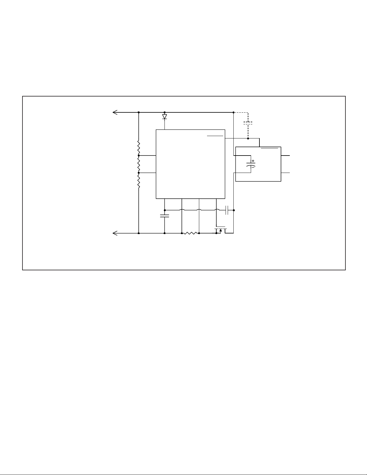
Application Information, cont’d.
Reverse Polarity Protection
The UV and OV pins are protected against reverse polarity input
supplies by internal clamping diodes and the fault currents are
sufficiently limited by the impedance of the external resistor
divider, however, a low current diode with a 100V breakdown
rating must be inserted in series with the VDD pin.
HV301/HV311
This method (shown in Application Circuit 12) will protect the
hotswap control circuit however, due to the intrinsic diode in the
external MOSFET, the load will not be protected from reverse
polarity voltages.
GND
8
V
DD
R1
-48V
487kΩ
R2
6.81kΩ
R3
9.76kΩ
3
2
C1
10nF
UV
OV
RAMP
Note: capacitor may be needed to slow PWRGD dv/dt if
oscillations are observed when V
is close to OV.
IN
D1
PWRGD / PWRGD
HV311
V
SENSE GATE
EE
574
R4
12.5mΩ
6
Q1
IRF530
1
ENABLE / ENABLE
Cload
+5V
DC/DC
PWM
CONVERTER
COM
Application Circuit 12
16
Page 17
Application Information, cont’d.
HV301/HV311
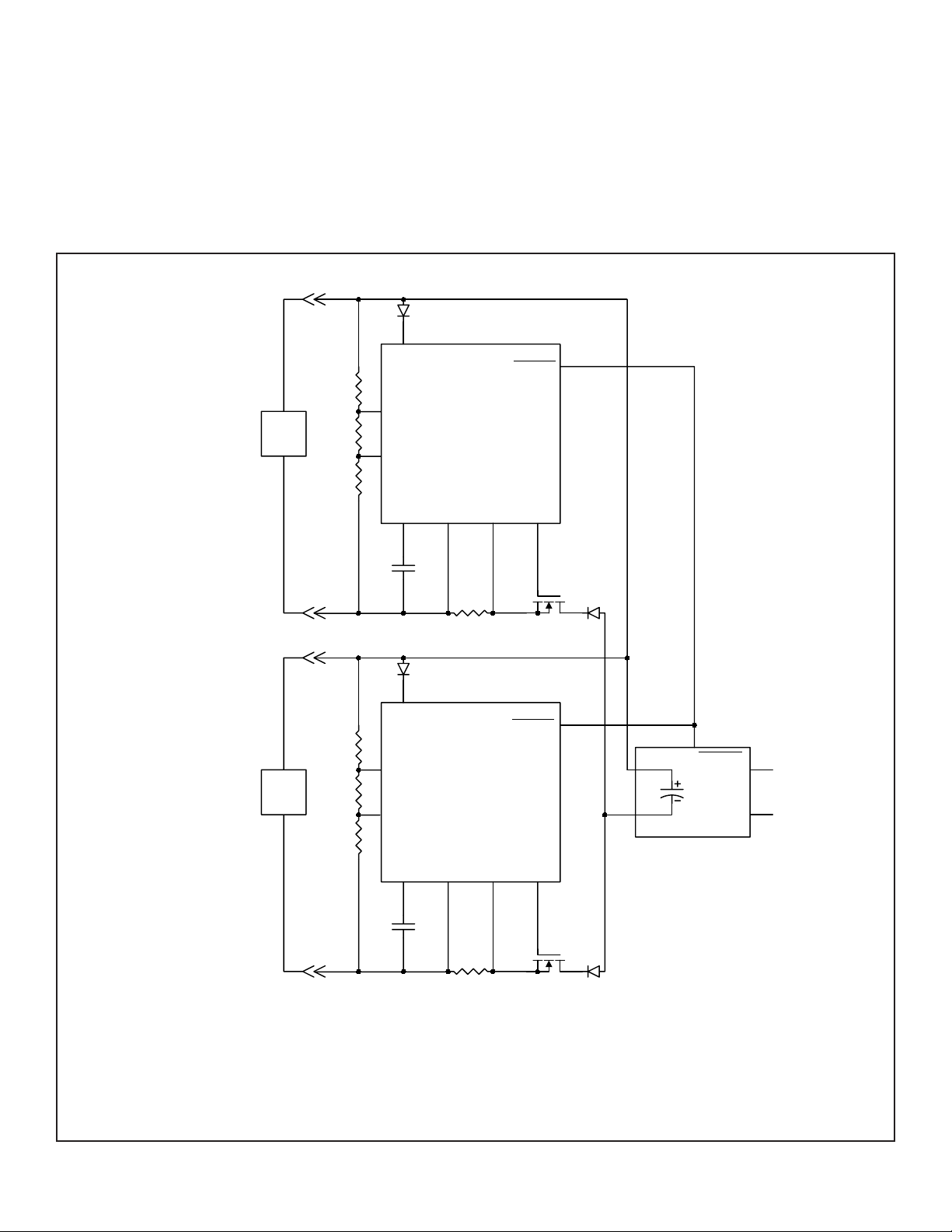
Redundant Supplies
Many systems use redundant primary power supplies or battery
backup. When redundant AC powered sources are used they are
generally diode OR’ed to the load on the hot terminal.
For these systems, the use of independent hotswap controllers
is recommended with the diode OR’ing provided after the hotswap
3
2
8
V
UV
OV
RAMP
DD
D2
C1
10nF
PS1
GND
487kΩ
6.81kΩ
9.76kΩ
-48V
R1
R2
R3
HV301/
HV311
V
EE
60mΩ
controllers. The HV311 is ideally suited for such applications
since two or more active low PWRGD signals can be connected
to a single active low ENABLE pin, thus enabling the load as long
as at least one primary power source is available. By adding low
current 100V diodes in series with the V
pins, full reverse
DD
polarity protection on either power source is also provided
(Application Circuit 13).
PWRGD
SENSE GATE
574
R4
6
Q1
IRF530
1
D1
D2
8
V
DD
3
UV
2
OV
RAMP
C1
10nF
PS2
GND
R1
487kΩ
R2
6.81kΩ
R3
9.76kΩ
-48V
Note: capacitor may be needed to slow PWRGD dv/dt if
oscillations are observed when VIN is close to OV.
HV301/
HV311
V
EE
60mΩ
PWRGD
SENSE GATE
574 6
R4
Q1
IRF530
1
ENABLE / ENABLE
Cload
DC/DC
PWM
CONVERTER
D1
+5V
COM
Application Circuit 13
17
Page 18
Application Information, cont’d.
HV301/HV311
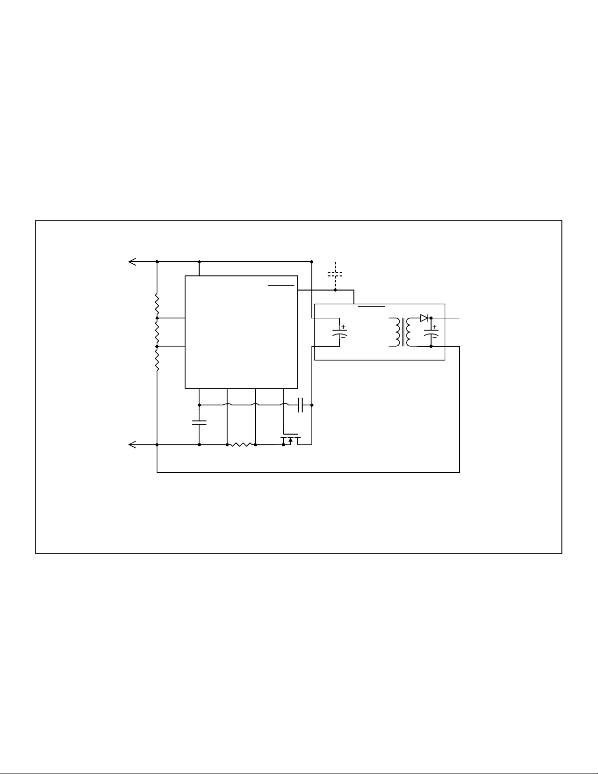
Use with Negative Ground
Either the HV301 or HV311 may be used with any negative
ground systems where DC/DC PWM Converters have isolated
outputs and their inputs need not be ground referenced
(Application Circuit 14).
+48V
487kΩ
6.81kΩ
9.76kΩ
R1
R2
R3
8
V
DD
3
UV
PWRGD / PWRGD
HV301/
2
OV
RAMP
HV311
V
EE
SENSE GATE
574
Current Limit Stability (Method 2 (Servo) Only)
The closed loop current mode control system used in the HV301/
HV311 is very stable, especially when driving MOSFETs with
high gate capacitances (C
). However, a peaking in I
ISS
LIMIT
near
the end of the current limit may be noted with some MOSFETs.
The current control loop can be frequency compensated to
eliminate this peaking by adding a series connected capacitor
and resistor between the gate and source of the external MOSFET.
The recommended starting values for C and R are 10nF and 1K.
These compensation values should be verified by board level
testing, which may yield satisfactory results with reduced component values.
1
ENABLE/ ENABLE
Cload
DC/DC PWM CONVERTER
6
+5V
COM
C1
GND
10nF
R4
12.5mΩ
Note: capacitor may be needed to slow PWRGD dv/dt if
oscillations are observed when VIN is close to OV.
Q1
IRF530
Application Circuit 14
18
Page 19
Application Information cont’d.
HV301/HV311
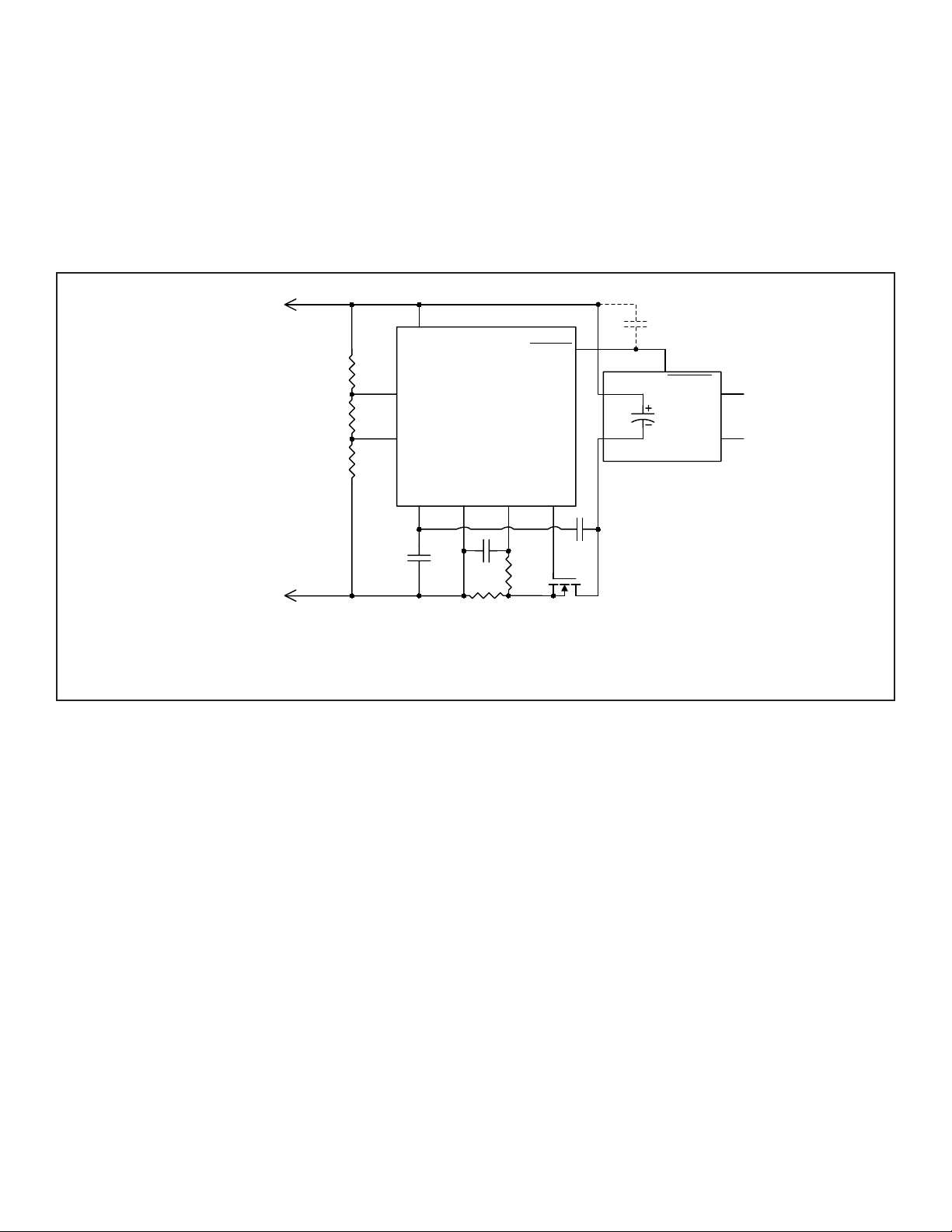
Extending Circuit Breaker Delay
Connecting a resistor in series with the SENSE pin and a
capacitor between the SENSE and VEE pins as shown in the
following diagram may be used to extend the Circuit Breaker
delay time beyond the 5µs internally set delay time (Application
Circuit 15).
The time delay achievable by this method is limited since this
GND
-48V
R1
487kΩ
R2
6.81kΩ
R3
9.76kΩ
8
V
DD
3
UV
2
OV
RAMP
delay circuit will also effect the current control feedback loop and
will result in a current overshoot during the external pass device
turn on transition to current limit. If the time delay required for the
Circuit Breaker causes excessive current overshoot during the
turn on transition then the following circuit may be used, where
the RC filter is switched on after the completion of the current
limit control function of the hotswap controller.
PWRGD / PWRGD
HV301/
HV311
V
SENSE GATE
EE
574
C2
R5
1
ENABLE/ ENABLE
Cload
DC/DC
PWM
CONVERTER
6
+5V
COM
Note: capacitor may be needed to slow PWRGD dv/dt if
oscillations are observed when VIN is close to OV.
R4
12.5mΩ
Q1
IRF530
Application Circuit 15
19
Page 20
Application Information cont’d.
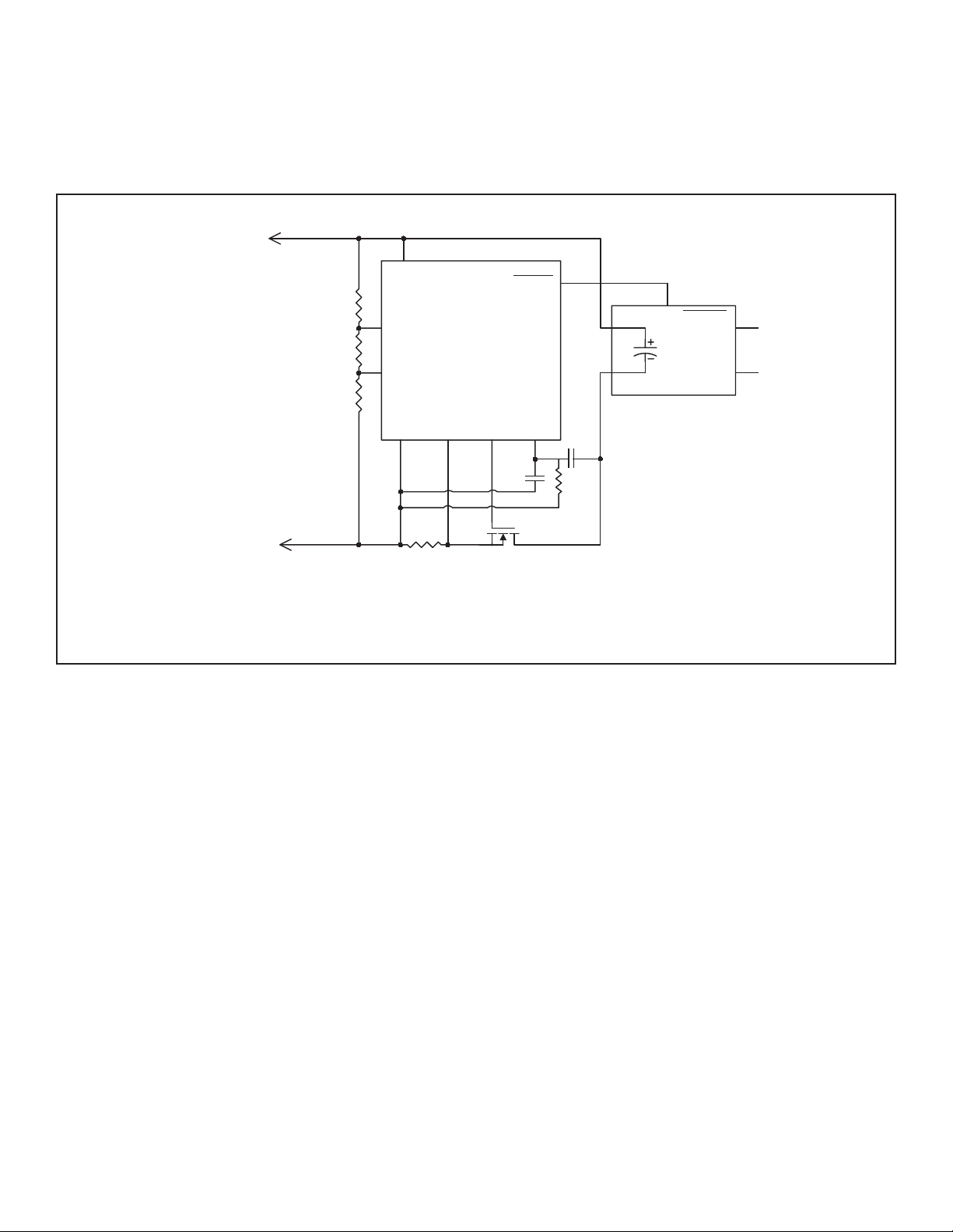
Latched Operation
For those applications that need to disable the automatic retry
capability, the following circuit disables the auto retry feature.
HV301/HV311
GND
R1
487kΩ
R2
6.81kΩ
R3
9.76kΩ
-48V
8
V
DD
3
UV
HV301 / HV311
2
OV
V
SENSE GATE
EE
R4
12.5mΩ
Note: capacitor may be needed to slow PWRGD dv/dt if
oscillations are observed when VIN is close to OV.
PWRGD / PWRGD
RAMP
645 7
Q1
IRF530
1
2.5MΩ
ENABLE / ENABLE
Cload
DC/DC
PWM
CONVERTER
+5V
COM
Application Circuit 17
20
Page 21
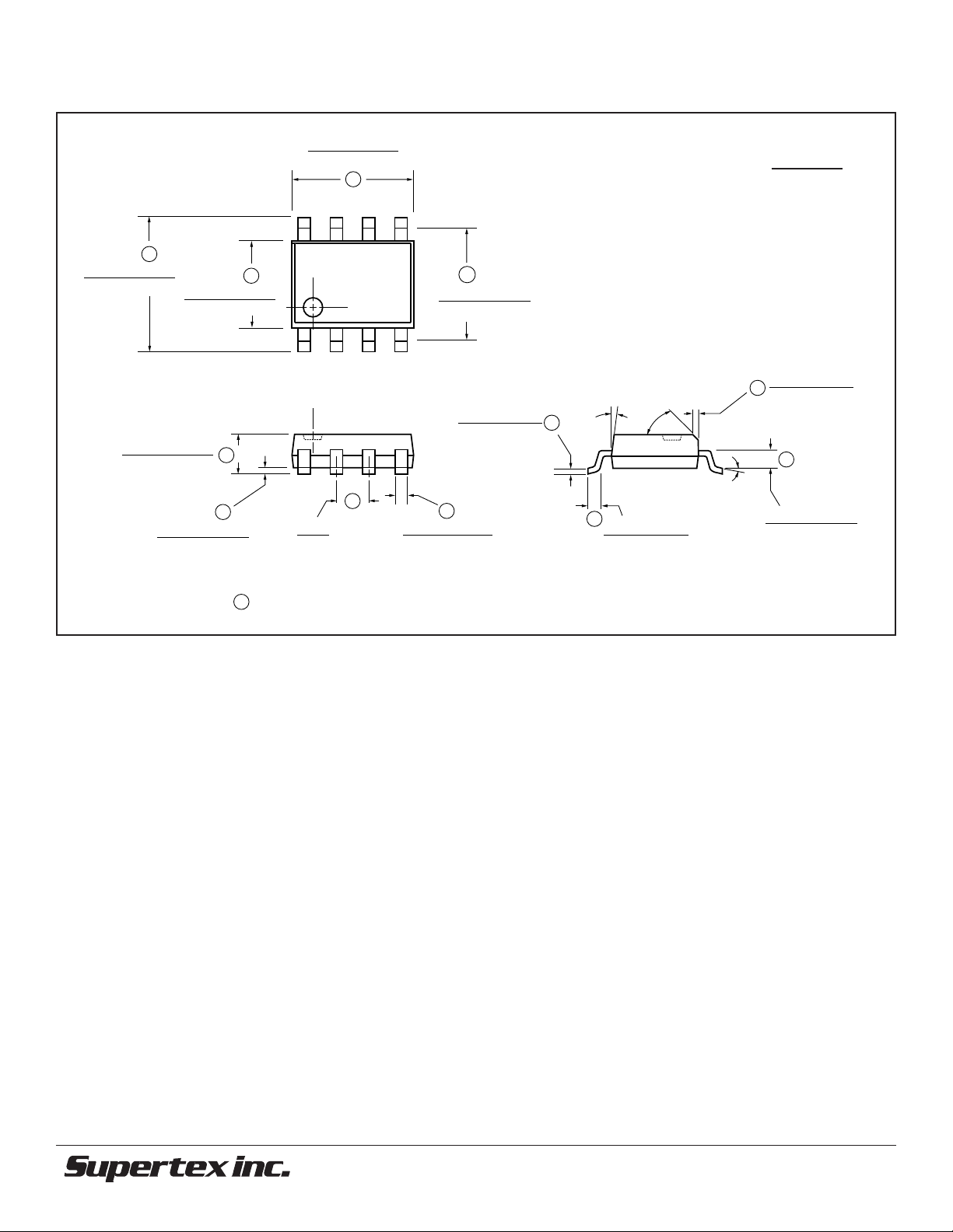
Package Dimensions
HV301/HV311
H
0.236 ± 0.008
(5.99 ± 0.20)
0.061 ± 0.008
(1.55 ± 0.20)
0.154 ± 0.004
(3.91 ± 0.10)
A
A
1
0.007 ± 0.003
(0.178 ± 0.076)
0.192 ± 0.005
(4.89 ± 0.11)
D
E
H
1
Inches
(Millimeters)
0.193 ± 0.012
(4.90 ± 0.30)
0.020 ± 0.009
h
(0.508 ± 0.229)
L
1
0.0275 ± 0.0025
(0.698 ± 0.064)
0.050
(1.20)
TYP.
7° (4 PLCS)
0.010 ± 0.002
(0.254 ± 0.051)
e
B
0.016 ± 0.002
(0.406 ± 0.05)
C
45°
0° – 8°
L
0.035 ± 0.015
(0.889 ± 0.381)
Circled letters (e.g. denote JEDEC reference dimensons.
B
©2002 Supertex Inc. All rights reserved. Unauthorized use or reproduction prohibited.
21
08/26/02 rev.11b
1235 Bordeaux Drive, Sunnyvale, CA 94089
TEL: (408) 744-0100 • FAX: (408) 222-4895
www.supertex.com
 Loading...