

Page 1
16 Channel High Voltage Analog Switch
Ordering Information
Package Options
V
PP-VNN
220V HV20822FG HV20822X
48-lead TQFP Die
HV20822
Features
❏ HVCMOS® technology for high performance
❏ 220V operating conditions
❏ Output On-resistance typically 22Ω
❏ 5.0V and 12.0V CMOS logic compatibility
❏ Very low quiescent power dissipation-10µA
❏ -45dB min off isolation at 7.5MHz
❏ Low parasitic capacitance
❏ Excellent noise immunity
❏ Flexible high voltage supplies
Absolute Maximum Ratings*
VDD Logic power supply voltage -0.5V to +15V
V
- VNN Supply voltage +225V
PP
V
Positive high voltage supply -0.5V to VNN +225V
PP
Negative high voltage supply +0.5V to -225V
V
NN
Logic input voltages -0.5V to V
V
Analog Signal Range VNN to V
SIG
Peak analog signal current/channel 3.0A
Storage temperature -65°C to +150°C
Power dissipation 48-lead TQFP 1.0W
* All voltages are referenced to ground. Absolute maximum ratings are those
values which damage to the device may occur. Functional operation under
these conditions is not implied. Continuous operation of the device at the
absolute rating level may affect device reliability.
+0.3V
DD
General Description
The Supertex HV208 is a 220V 16-channel high-voltage analog
switch integrated circuit (IC) configured as 2 sets of 8 single pole
single throw analog switches. It is intended for use in applications requiring high voltage switching controlled by low voltage
control signals such as ultrasound imaging and printers. The 2
sets of 8 analog switches are controlled by 2 input logic controls,
1 and DIN2. A logic high on DIN1 will turn ON switches 0 to 7
D
IN
and a logic high on D
PP
2 will turn ON switches 8 to 15.
IN
06/26/01
Supertex Inc. does not recommend the use of its products in life support applications and will not knowingly sell its products for use in such applications unless it receives an adequate "products liability
indemnification insurance agreement." Supertex does not assume responsibility for use of devices described and limits its liability to the replacement of devices determined to be defective due to
workmanship. No responsibility is assumed for possible omissions or inaccuracies. Circuitry and specifications are subject to change without notice. For the latest product specifications, refer to the
Supertex website: http://www.supertex.com. For complete liability information on all Supertex products, refer to the most current databook or to the Legal/Disclaimer page on the Supertex website.
1
Page 2
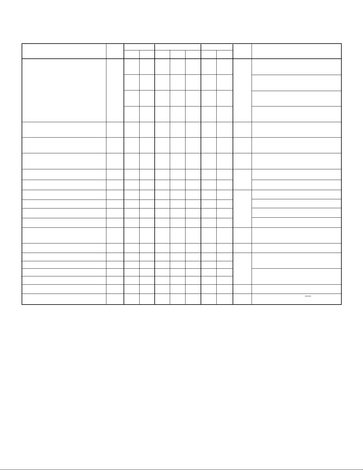
Electrical Characteristics
DC Characteristics (over recommended operating conditions unless otherwise noted)
°C+25°C+70°C
Characteristics Sym Units Test Conditions
Small Signal Switch (ON) R
ONS
Resistance V
Small Signal Switch (ON) ∆R
ONS
Resistance Matching V
Large Signal Switch (ON) R
ONL
Resistance
Switch Off Leakage I
SOL
Per Switch
DC Offset Switch OFF 300 100 300 300
DC Offset Switch ON 500 100 500 500 R
Pos. HV Supply Current I
Neg. HV Supply Current I
Pos. HV Supply Current I
Neg. HV Supply Current I
PPQ
NNQ
PPQ
NNQ
Switch Output Peak Current 3.0 3.0 2.0 2.0 A V
0
min max min typ max min max
30 26 32 40 V
25 22 27 35 V
15 22 27 30 V
20 18 22 25 V
20 5.0 20 20 % V
15 ohms V
5.0 1.0 10 15 µAV
10 50 All SWs OFF
-10 -50 µA All SWs OFF
10 50 All SWs ON, I
-10 -50 All SWs ON, I
ohms V
mV
= 0V, I
SIG
= 50V, V
PP
SIG
= 50V, VNN = -170V
PP
SIG
= 110V, V
V
PP
SIG
= 110V, V
V
PP
SIG
= 110V, V
PP
SIG
SIG
R
= 100Kohms
L
= 100Kohms
L
SIG
SIG
= 0V, I
SIG
= 0V, I
SIG
= 0V, I
SIG
= 0V, I
SIG
= 0V, I
SIG
= VPP -10V and VNN +10V
duty cycle ≤ 0.1%
= 5mA,
= -170V
NN
= 200mA,
= 5mA,
= -110V
NN
= 200mA,
= -110V
NN
= 5mA,
= -110V
NN
= 1.0A
= 5 mA
SW
= 5 mA
SW
HV20822
Output Switch Frequency f
I
Supply Current I
PP
Supply Current I
I
NN
IPP Supply Current I
Supply Current I
I
NN
Logic Supply Quiescent Current I
Logic Supply Average Current I
SW
PP
NN
PP
NN
DDQ
DD
50 KHz Duty Cycle = 50%
8.1 8.8 10
-8.1 -8.8 -10
5 6.3 6.9
VPP = 50V, VNN = -170V, ALL SWs
turning ON and OFF at 50KHz
mA
V
= 110V, VNN = -110V, All SWs
PP
-5 -6.3 -6.9 turning ON and OFF at 50kHz
10 10 10 µA All logic states are at DC
2.0 2.0 2.0 mA DIN1 = DIN2 = 3MHz, LE = high
2
Page 3
HV20822
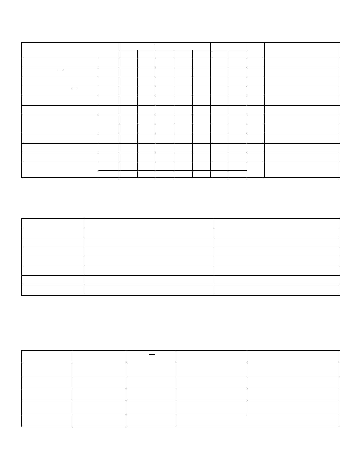
Electrical Characteristics
AC Characteristics (over recommended operating conditions unless otherwise noted)
Characteristics Sym Units Test Conditions
Time to Turn OFF V
Time Width of LE t
Time Width of D
Set Up Time Before LE Rises t
Turn On Time t
Turn Off Time t
*t
SIG
IN
SIG(OFF)
WLE
t
WDIN
SD
ON
OFF
Off Isolation KO -30 -30 -33 -30 dB f = 5.0MHz, 1KΩ/15pF Load
Switch Crosstalk K
Off Capacitance Switch to GND C
On Capacitance Switch to GND C
Output Voltage Spike +V
*Time required for analog signal to turn off before output switch turns off.
CR
GS(OFF)
GS(ON)
SPK
-V
SPK
0°C +25°C +70°C
min max min typ max min max
00 0ns
150 150 150 ns
150 150 150 ns
150 150 150 ns
2.0 2.0 2.0 µsV
2.0 2.0 2.0 µsV
SIG=VPP
SIG=VPP
- 10V, R
- 10V, R
-45 -45 -50 -45 dB f = 7.5MHz, R
-45 -45 -45 dB f = 5.0MHz, R
5.0 17 5.0 12 17 5.0 17 pF V
25 50 25 38 50 25 50 pF V
= 0V, 1MHz
SIG
= 0V, 1MHz
SIG
4.0 V
-4.0
LOAD
LOAD
=10KΩ
LOAD
=10KΩ
LOAD
= 50Ω
= 50Ω
Operating Conditions
Symbol Parameter Value
V
PP
V
NN
V
DD
V
IH
V
IL
V
SIG
T
A
Notes:
1 Power up/down sequence is arbitrary except GND must be powered-up first and powered-down last.
must be VNN ≤ V
2V
SIG
≤ VPP or floating during power up/down transition.
SIG
Positive high voltage supply
Negative high voltage supply
Logic power supply voltage
High-level input voltage VDD -1.0V to V
Low-level input voltage 0V to 1.0V
Analog signal voltage peak-to-peak
Operating free air-temperature 0°C to 70°C
1
1
1
2
+50V to +110V
-10V to VPP-220V
4.75V to +12.6V
DD
VNN +10V to VPP -10V
Truth Table
DIN2 DIN1 LE SW0 to SW7 SW8 to SW15
L L L OFF OFF
L H L ON OFF
H L L OFF ON
H H L ON ON
X X H HOLD PREVIOUS STATE
3
Page 4
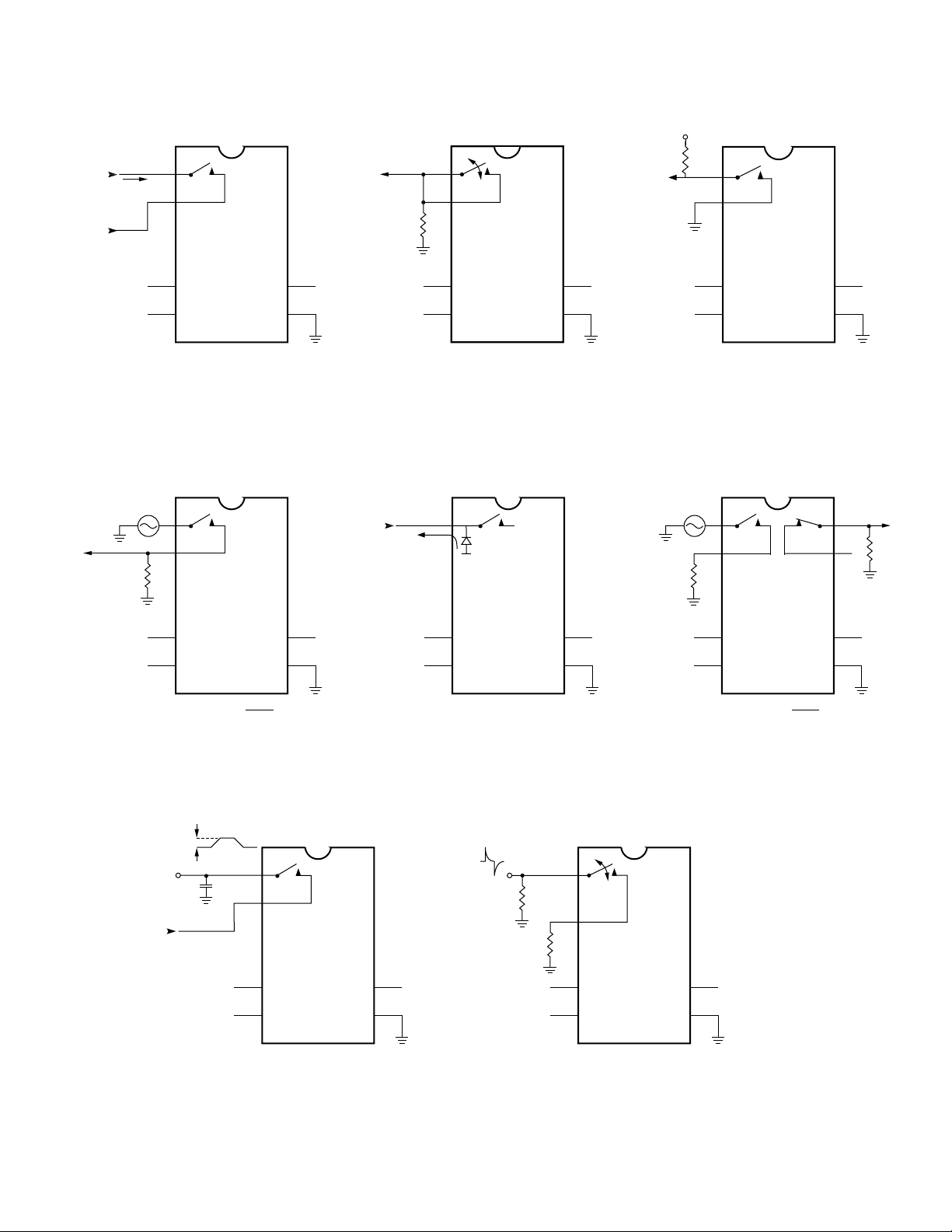
Test Circuits
I
SOL
–10
V
PP
HV20822
VPP –10V
R
10KΩ
V
OUT
L
V
OUT
VNN +10
V
OUT
VIN = 10 V
@5MHz
V
PP
V
NN
V
PP
V
NN
Switch OFF Leakage
P–P
R
L
V
PP
V
NN
V
PP
V
NN
V
GND
V
GND
100KΩ R
DD
5V
V
SIG
L
V
PP
V
NN
V
PP
V
NN
DC Offset ON/OFF
I
ID
V
NN
V
GND
DD
5V
V
PP
V
NN
VIN = 10 V
@5MHz
P–P
V
PP
V
NN
TON/T
Test Circuit
OFF
V
GND
DD
5V
50Ω
NC
50Ω
DD
5V
V
PP
V
NN
V
PP
V
NN
V
GND
DD
5V
V
PP
V
NN
V
PP
V
NN
V
GND
DD
5V
V
V
SIG
∆V
OUT
OUT
1000pF
V
KO = 20Log
OUT
V
IN
OFF Isolation
V
PP
V
NN
Charge Injection
V
PP
V
NN
Q = 1000pF x ∆V
V
GND
OUT
V
V
OUT
IN
Isolation Diode Current
+V
SPK
V
OUT
–V
SPK
KCR = 20Log
Crosstalk
50Ω
1KΩ R
L
DD
5V
V
PP
V
NN
V
PP
V
NN
V
GND
DD
5V
Output Voltage Spike
4
Page 5
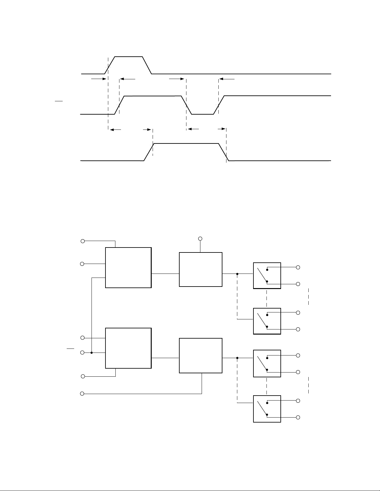
Logic Timing Waveform
V
D
LE
DD
IN
0V
V
DD
0V
50%
t
sd
50% 50% 50%
t
WLE
HV20822
ON
SW
OFF
Block Diagram
V
DD
DIN1
t
ON
Latch
1
90%
t
V
PP
Level
Trans 1
OFF
10%
SW0
SW0
DIN2
LE
GND
V
NN
Latch
2
Level
Trans 2
5
SW7
SW7
SW8
SW8
SW15
SW15
Page 6
HV20822
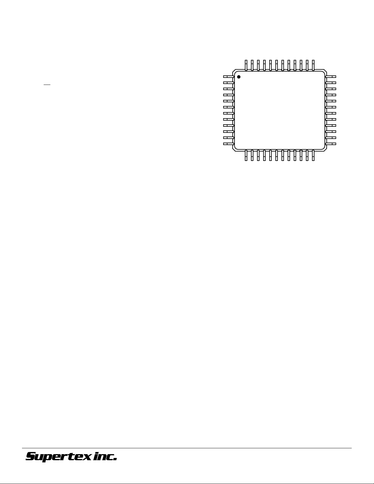
Pin Configuration
HV208 48-Pin TQFP
Pin Function
1V
NN
2 N/C
3V
PP
4 N/C
5D
1
IN
6LE
7D
2
IN
8 N/C
9 N/C
10 V
DD
11 GND
12 N/C
13 N/C
14 SW15
15 SW15
16 SW14
17 SW14
18 SW13
19 SW13
20 SW12
21 SW12
22 SW11
23 SW11
24 N/C
Pin Function
25 SW10
26 SW10
27 SW9
28 SW9
29 SW8
30 SW8
31 SW7
32 SW7
33 SW6
34 SW6
35 SW5
36 SW5
37 SW4
38 N/C
39 SW4
40 N/C
41 SW3
42 SW3
43 SW2
44 SW2
45 SW1
46 SW1
47 SW0
48 SW0
Package Outline
Pin 1
HV208
Pin #1
Pin 12
top view
48-pin TQFP
©2001 Supertex Inc. All rights reserved. Unauthorized use or reproduction prohibited.
06/26/01
1235 Bordeaux Drive, Sunnyvale, CA 94089
TEL: (408) 744-0100 • FAX: (408) 222-4895
6
www.supertex.com
 Loading...