

Page 1
Hologram Unit
,,
,,
HUL7001
Hologram Unit
For optical information processing
Features
Smaller package size achieved through
micro-mirror integration
(4.8 × 8.2 × 4.3 mm)
Focus error signal detection : SSD method
Tracking error signal detection
: 3-beam method
Low-power semiconductor laser included
Applications
CD
Absolute Maximum Ratings (Ta = 25˚C)
Parameter Symbol Ratings Unit
Laser beam output P
Laser reverse voltage V
Monitor PD reverse voltage V
Signal processing PD reverse voltage
Operating ambient temperature
Storage temperature T
O
R(LD)
R(mon)
V
R
T
opr
stg
– 10 to +60 ˚C
– 40 to +85 ˚C
1
2
3
4
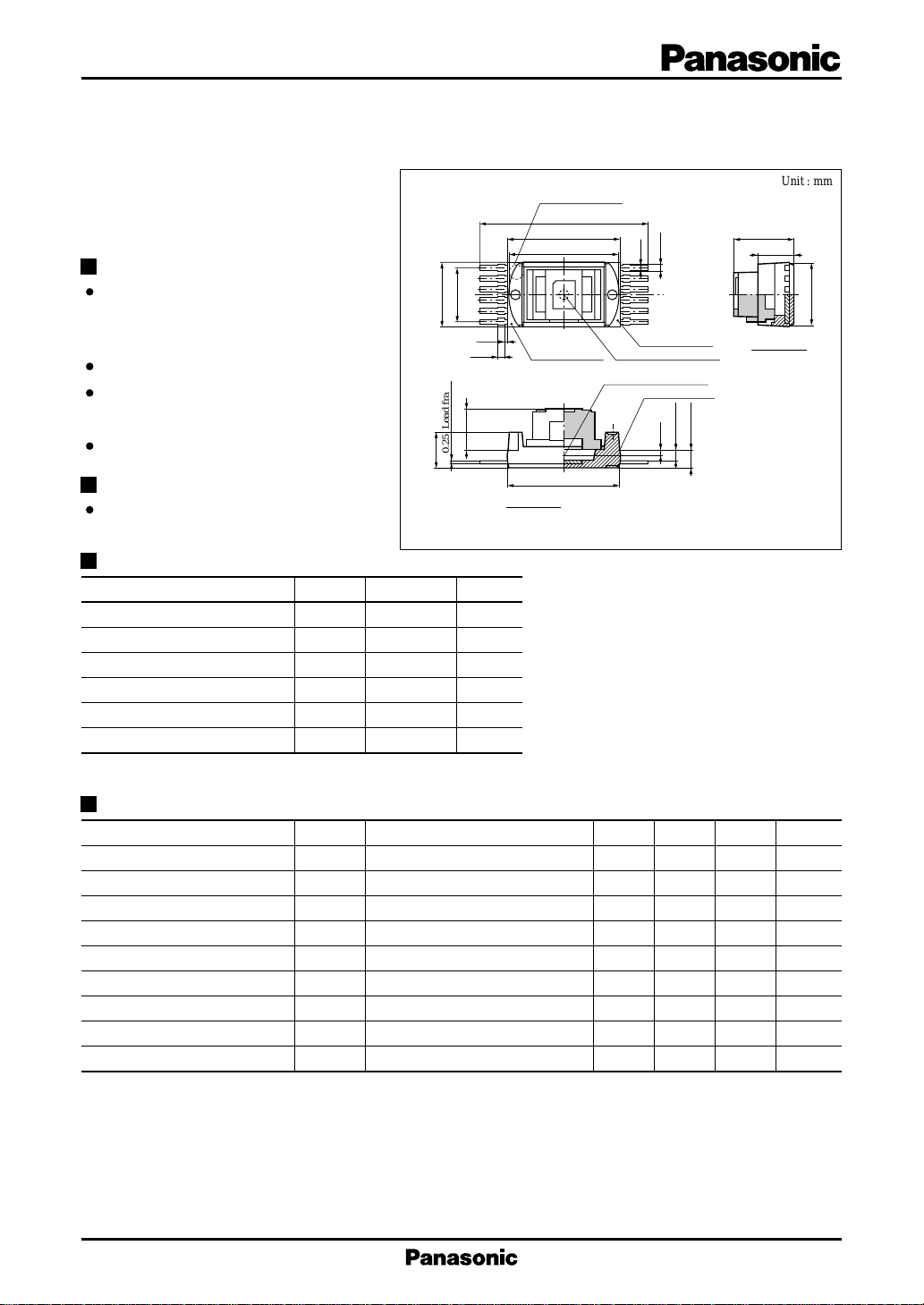
4.8±0.1
5
6
0.8×5=4.0±0.2
(0.2)
(0.5)
3.0±0.2
0.25 Lead frame
2.55±0.2
Reference plane
SEC. X-O-Y
0.3 mW
2V
12 V
12 V
Index mark for No.1
pin on reverse side
11.2±0.2
8.2±0.2
+0
ø8.0
–0.05
O
Y
8.1±0.2
(Note): 1.Standard corner R=0.20 max.
2.Thickness of plate:Ni 1µm min.+Au 0.1µm min.
3.Thickness of hologram=2.0mm, n=1.519
(0.35)
(0.3)
12
11
10
X
9
8
7
Reference plane
Apparent emitting point
Apparent emitting point
Reference plane
1.33±0.2
0.78±0.2
0.50
Unit : mm
4.33±0.2
2.55±0.2
4.7±0.1
SEC. X-O-Y
Unit Characteristic Specifications (Tc = 25 ± 3˚C)
Parameter Symbol Conditions min typ max Unit
Threshold current I
Operating current I
Operating voltage V
Laser beam output P
Focus error signal amplitude
Tracking error signal amplitude
Focus error signal defocusing
Tracking error signal symmetry
Focus error signal pull-in range
*1
Measurements are made using the reference optical system during measurement and the radiant power measurement system on
the hologram unit shown in Fig. 2.
*2
It should be noted that the RF signal amplitude in these specifications is denoted by IRF, and represents the amplitude of the 11T
signal. As in the case described in *1, IRF is measured using the measurement system shown in Fig. 2.
*3
The definition is illustrated in Fig. 3.
*4
The definition is illustrated in Fig. 4.
*5
The definition is illustrated in Fig. 5.
*1
th
OP
OP
O
I
FE
I
TE
D
FO
B
TE
D
FE
CW 20 30 40 mA
*1,2
CW IRF = 10µA, VR = 5V 25 35 45 mA
*1,2
CW IRF = 10µA, VR = 5V 1.9 2.4 V
*1,2
IRF = 10µA, VR = 5V 0.15 0.22 mW
*1,3
IRF = 10µA, VR = 5V 7 10 13 µ A
*1,4
IRF = 10µA, VR = 5V 0.8 1.3 1.8 µA
*1,5
IRF = 10µA, VR = 5V – 8 + 8 %
*1,4
IRF = 10µA, VR = 5V – 30 + 30 %
*1,3
IRF = 10µA, VR = 5V 12 µm
1
Page 2
HUL7001 Hologram Unit
Characteristic Specifications for Semiconductor Laser, Monitor PD, and Signaling Processing PD
Parameter Symbol Conditions min typ max Unit
Semiconductor laser
Oscillating wavelength λ
Coherence λ
Monitor PD and signal processing PD
Monitor current I
Dark current
Capacitance between pinss
Shield frequency f
*6
Measurements are made using the radiant power measurement system on the hologram unit. The definition is presented in Fig. 2.
*7
Unless otherwise indicated, the values shown are per individual element.
*8
The subscript (mon) denotes the element (monitor PD).
*9
C
denotes the capacitance measured at pin No. 4 or 10 in the electrode connection diagram. C
t(RF1)
measured at pin No. 5 or 9 in the electrode connection diagram.
*6
L
P(mon)
I
I
D(mon)
C
t(RF1)
C
t(RF2)
CW IRF = 10µA, VR = 5V 775 790 805 nm
*6
CW IRF = 10µA, VR = 5V 0.5 0.9
*7
CW IRF = 10µA, VR = 5V 0.3 0.7 1.2 mA
VR = 2.5V 0.2 3.0 nA
D
*8
VR = 5V 0.3 30 nA
*9
VR = 2.5V, f = 1MHz
*9
VR = 2.5V, RL = 50Ω 40 MHz
C
(Tc = 25±3˚C)
2pF
3pF
denotes the capacitance
t(RF2)
Connection Diagram (Fig. 1)
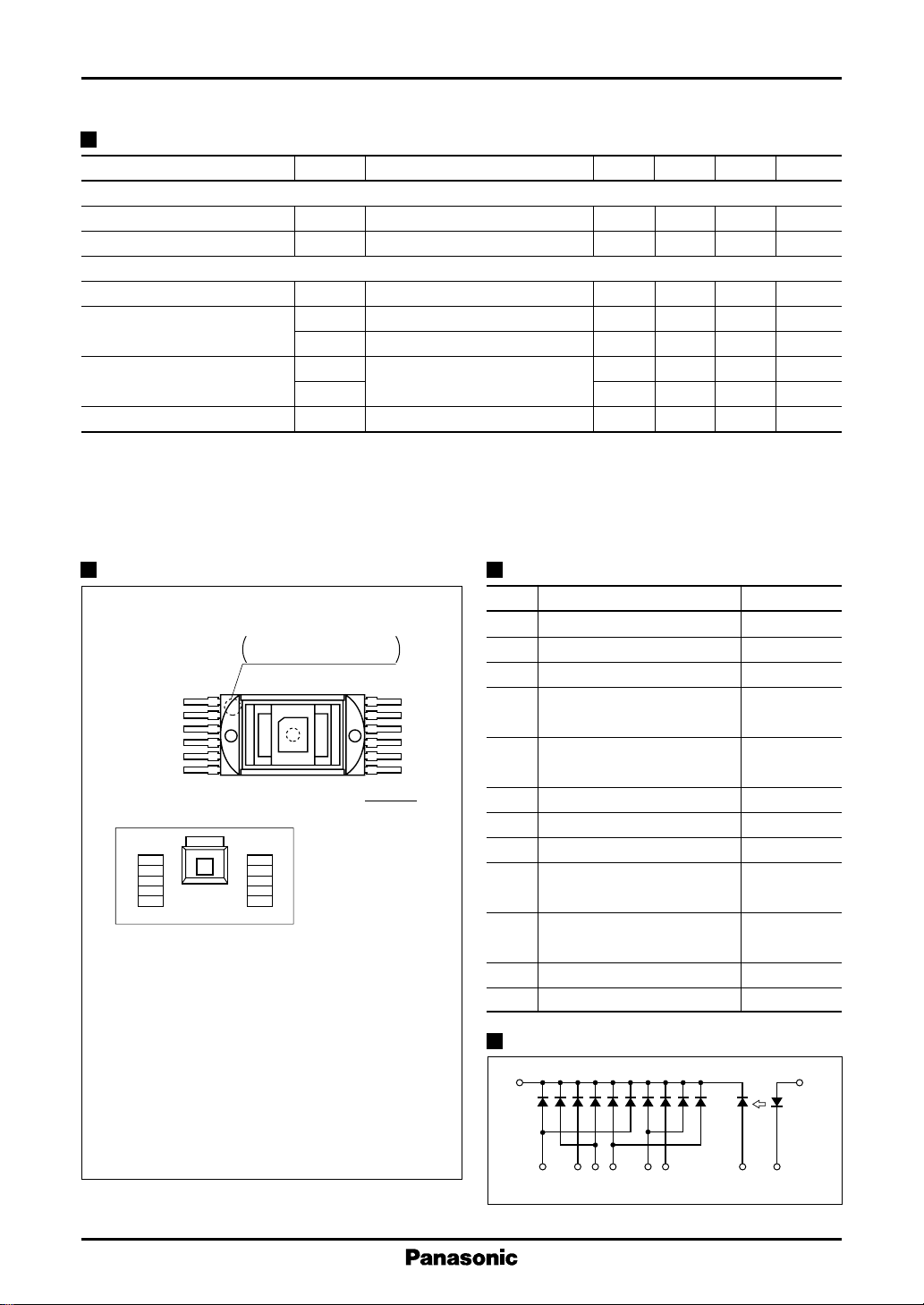
(a) Pin arrangement
Pin No.
(b) Chip structure
PD output current In :
detecting element N (n : 1 to 10, N = P1 to P10 )
Monitor PD output current I
received by Pmon element
Focus error signal FE = (I
Tracking error signal TE = (I
RF signal RF = I2+I3+I4+I7+I8+I
1
2
3
4
5
6
Pmon
P1
LD
P2
P3
P4
P5
Output current when light is received by light
Gritty face
Represents No.1 pin
carved seal on reverse side
TOP VIEW
LD
:
P6
P7
P8
P9
P10
: Output current when light is
P (mon)
2+I4+I8
Disk-close FE > 0
Disk-far FE < 0
1+I6
The leading beam is the beam received
by light detecting elements P1 and P6.
Semiconductor laser chip
: Monitor light detecting
Pmon
element
P1 ~ P10
: Signal-detection light detecting-elements
) – (I3+I7+I9)
) – (I5+I10)
9
12
11
10
9
8
7
Pin Description
Pin No.
1
Source voltage Applications pin
2 Monitor current output pin I
3
Tracking error signal output pin
RF and focus error signal
4
output pin
RF and focus error signal
5
output pin
6
Source voltage Applications pin
7
Source voltage Applications pin
8
Tracking error signal output pin
RF and focus error signal
9
output pin
RF and focus error signal
10
output pin
11 LD + Power supply pin
12 GND pin
Function Calculation
Electrode Connection Diagram
1,6,7
P1 P2 P3 P4 P5 P6 P7 P8 P9
)
(V
R
348910 2125
Pmon LD
P10
P (mon)
I1 + I
I
I2 + I
I5 + I
I7 + I
I
GND
6
3
4
10
9
8
11
LD+
2
Page 3
Hologram Unit HUL7001
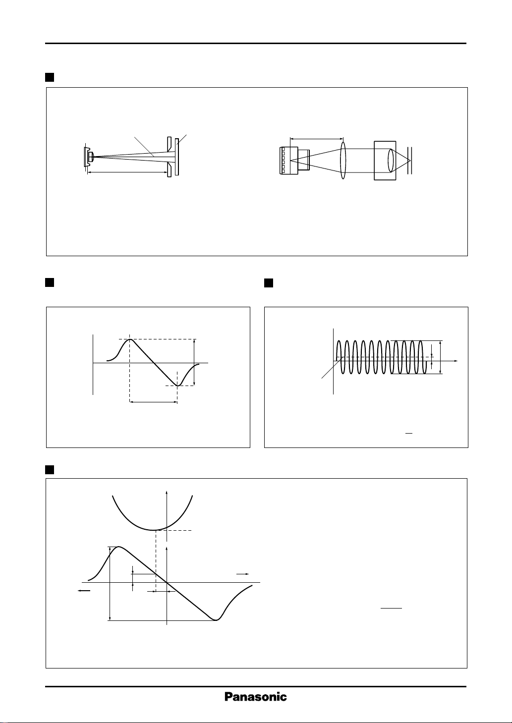
Optical Block Diagram During Measurement (Fig. 2)
(a) Radiant power measurement system of
hologram unit (HUL7001)
Hologram unit
(HUL7001)
PKG reference surface
(Note) The aperture and the light detecting element
are positioned perpendicular to the axis of
the light emitted from the hologram unit;
the optical axis is positioned so as to pass
through the center of the aperture.
Optical axis
19.0mm
Light detecting element
(ø10mm) or laser light
input element of coherence
measurement system
ø
3.1mm
aperture
The RF signal, focus error signal, and tracking error signal are measured using
the above reference optical system and the equations shown in Fig. 1.
Focus Error Signal Amplitude and Pull-in
Range (Fig. 3)
Focus error
signal
I
FE
Objective lens
movement
D
FE
(b) Reference optical system during measurement
Apparent light emitting point
25.3mm
Collimator lens Objective lens
f = 25.3mm
NA = 0.105
Actuator
f = 4.5mm
NA = 0.45
Disk :
A disk satisfying
CD specifications
is used.
Tracking Error Signal Amplitude and Pull-in
Range (Fig. 4)
Tracking error
signal strength
Signal amplitude
center ground level
+
B
0
–
A : Tracking signal amplitude
B :
Difference between tracking signal
amplitude center and electrical center
A
Time
I
: Focus error signal amplitude
FE
D
: Focus error signal pull-in range
FE
Focus Error Signal Defocusing (Fig. 5)
High
Jitter
(ns)
Low
Focus error signal
+
Moving away from disk
Approaching disk
S
(DJ)
0
D
I
FE
J
–
In the diagram, point 0 is the point at
which the focus error signal equals 0.
Tracking error signal amplitude I
Tracking error signal symmetry B
DJ : Objective lens movement from position where focus error signal
is 0 to jittering-best position.
S
: Amount of focus error signal at D
(D
)
J
IFE : Focus error signal amplitude
J
= A
TE
B
= ×100 (%)
TE
A
Objective lens
movement (µA)
Focus error signal
defocusing D
FO
S
(DJ)
=
I
EF
×100 (%)
(Definition of focus error signal defocusing)
Amount of focus error signal at jitter-best position as
a percentage of focus error signal amplitude (%)
3
Page 4

HUL7001 Hologram Unit
Important LDHU Usage Information
Panasonic’s laser detector hologram unit (LDHU)
has features of using a plastic package, and of integrating a low-current-operating, high-efficiency laser and a photodetector in order to reduce the size
and weight of the optical pickup.
Please follow the instructions presented below to
take advantage of this feature and ensure that the
pickup is highly reliable.
1. Static Electricity
The semiconductor laser used in the LDHU is characteristically, especially sensitive to static electricity, in semiconductor devices. Therefore care must
be taken in handling the semiconductor laser. If the
laser receives a pulse which causes light to be emitted in excess of the maximum rating of the laser, the
laser itself could be damaged by the optical energy.
Therefore it is very important to take measures to
protect the LDHU from static electricity and surges
when putting together assembly lines or when handling it during manufacturing processes.
(1) Check all drive circuitry, including the power sup-
ply. Take sufficient preventive measures to ensure that, for example, spike currents generated
when the power switch is turned on or off never
exceed the absolute maximum ratings of the
LDHU. Also insert appropriate protective circuits
in the LDHU drive circuitry.
(2) Be careful not to allow static electricity to de-
stroy the LDHU while handling it. Effective measures for protecting against static electricity include body grounds (passing through 1MΩ), as
well as conductive mats for the floor, conductive
clothing, conductive shoes, and conductive containers. The tips of soldering irons must be
grounded. We recommend using ionizers, etc.,
especially around facilities and areas where static
electricity is easily generated.
2. LDHU Heat-Release Design
The semiconductor laser, which is the light emitting device, naturally has a limited service life. This
service life is shortened as the temperature is increased. Therefore the design should include suitable heat-releasing measures. Heat release from the
lead frame and the back of the package must be incorporated into the design in order to improve heatreleasing capabilities. For assistance in evaluating
heat-releasing capabilities (thermal resistance), please
contact us.
3. Storing LDHU Units After Removal from Aluminum-Laminated Bags
If supplies are stored prior to mounting for extended periods of time in a high-humidity environment, subsequent heating during solder mounting will
cause moisture in the parts to vaporize. This may
cause problems related to part characteristics.
In order to prevent moisture absorption, LDHU
units are packaged in moistureproof aluminum-laminated bags which are sealed together with silica gel
before shipping. After LDHU units are removed from
these moistureproof bags, the mounting process
should be completed quickly. Unused LDHU units
which have been unsealed and require extended storage should be put back in their aluminum-laminated
bags (along with the silicagel) and resealed.
The recommended environment for LDHU mounting is a temperature range of 5˚C to 35˚C and a relative humidity range of 45% to75%. (To prevent excessive humidity and because static electricity occurs more easily if the humidity is too low.)
(3) The laser may also be destroyed by abnormal
pulses from nearby equipment. Therefore fluorescent lights and measuring equipments should
not be turned on or off near the laser.
4
Page 5
Hologram Unit HUL7001
4. Important Information Regarding Soldering
Special plastics are used in the LDHU package
and hologram. Therefore only the leads (pins)
should be heated (during soldering iron, dip, etc.),
and soldering time should be short. Total heating
methods such as reflow soldering should be
avoided. (This device is gold-plated to ensure
good solder adhesion, so a short soldering time is
sufficient.) It is also recommended that a heat
sink or other means be used to improve the
package’s heat-releasing effects in order to prevent the package from becoming hot as a result of
heat transfer and radiation even when the leads
are heated.
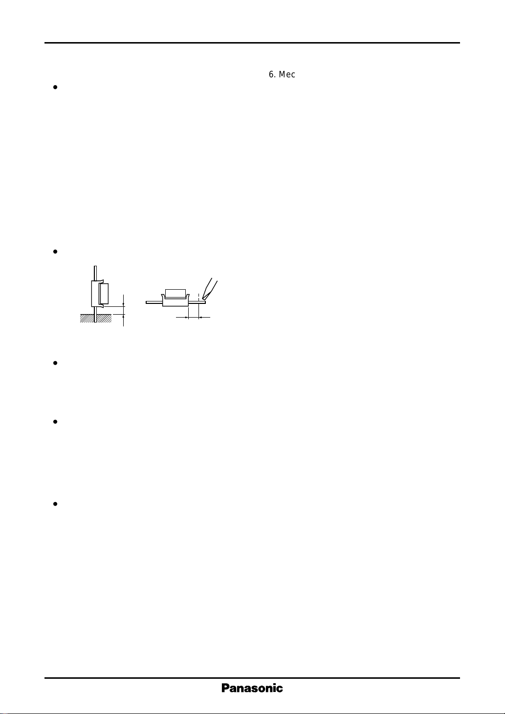
Soldering location
A
A
A : Make sure there is a gap of at least 1mm.
Soldering temperature and time
Temperature : 260˚C maximum
Time : 5 seconds maximum
5. Flux cleaning method
Alcohol is recommended as a solvent for flux clean-
ing. Chlorine base solvents in particular are a
cause of lead corrosion and device deterioration.
Petroleum base solvents should be avoided since
they deteriorate the adhesive between the hologram and package.
6. Mechanical stress
(1) Pressure on the package
The LDHU package is made thin in order to reduce its size. Therefore, pressure on the package
resulting of heat release, etc. may cause problems
such as a change in the package shape or changes
to its characteristics. In the point pressure application, force should be limited to 1kgf (9.8N) or
less, but please design so that the area pressure
application can be adopted as much as possible.
(2) Lead formation and cutting
In cases where lead formation and cutting are required, these actions must be performed at normal temperatures prior to soldering. Machining
steps performed at high temperatures immediately
after soldering, or after the solder has hardened
should be avoided. In addition, steps should be
taken to ensure that excessive mechanical stress
is not applied during lead formation and cutting.
Special care should be taken to avoid stress on
the lead bases of the package, as this may create
problems such as chipping the resin.
7. Other issues
(1) The surface of the hologram is very important for
light emission and light detecting. Therefore care
should be taken to ensure that there are no fingerprints on the surface, residual flux after soldering, or adhering dust.
(2) V iewing the laser beam with the naked eye is ex-
tremely dangerous and may result in blindness.
Do not look directly at the laser while it is operating.
In addition, ultrasonic cleaning should be avoided
since the device is hollow. Care should be taken
in brushing the hologram surface, as this may
scratch the back side.
(3) The products listed in this document are intended
for use in standard applications, i.e., general electronic devices (such as office equipment, measuring equipment, and consumer electronics products). Customers considering applications involving special quality and reliability requirements and
carrying a risk of loss of human life or bodily damage in the event of an accident or malfunction, or
specific applications (such as aerospace applications, transportation equipment, combustion
equipment, and safety devices), and customers
considering applications other than the standard
applications intended by us should contact our
sales office before using these products.
5
 Loading...