

Page 1
Features
•
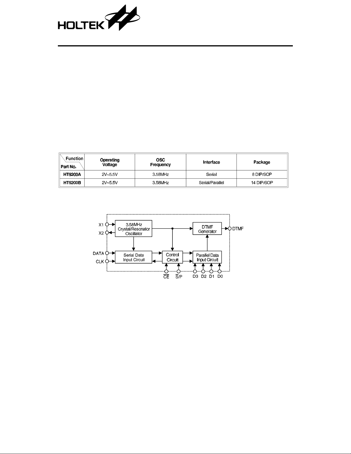
Operating voltage: 2.0V ~5.5V
•
Serial mode for the HT9200A
•
Serial/parallel mode for the HT9200B
General Description
The HT9200 A/B tone generators are d esigned
for
µC interfaces. They can be instru cted by a
µC to generate 16 dual tones and 8 single tones
from the DTMF p in. The HT9200A provides a
serial mode wh ereas the HT9200B conta ins a
Selection Table
HT9200A/B
DTMF Generators
•
Low standby current
•
Low total harmonic distortion
•
3.58MHz crystal or ceramic resonator
selectable serial/parallel mode interface for
various appl ications such as security systems,
home automation , remote control thro ugh tele phone lines, communication systems, etc.
Block Diagram
1 21st Aug ’98
Page 2
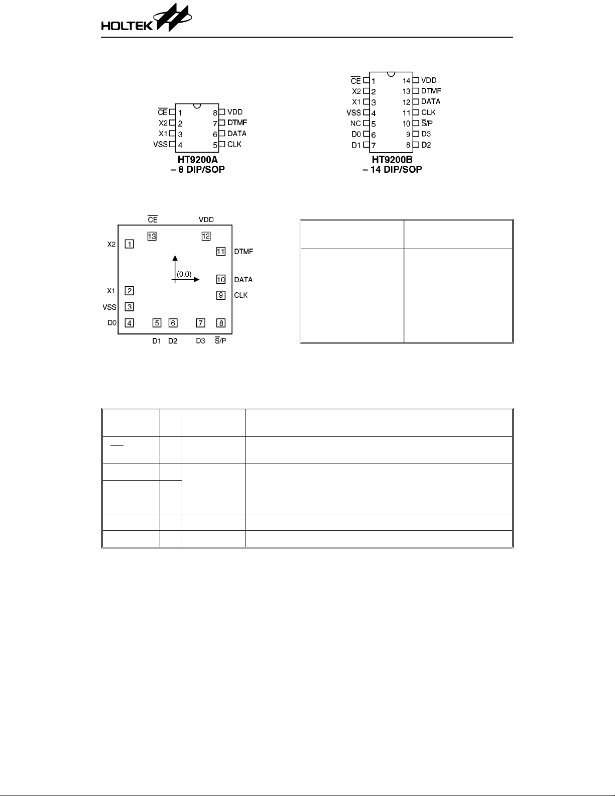
Pin Assignment
HT9200A/B
Pad Assignment Pad Coordinates
Pad
No.
1 –553.30 430.40 8 553.30 –523.50
2 –553.30 –133.50 9 553.30 –190.30
3 –553.30 –328.50 10 553.30 4.70
4 –553.30 –523.50 11 553.30 340.30
5 –220.10 –523.50 12 374.90 523.50
6 –25.10 –523.50 13 –279.30 523.50
7 308.10 –523.50
Chip size: 1460
* The IC substrate should be connected to VSS in the PCB layout artwork.
× 1470 (µm)
2
XY
Pin Description
Pin Name I/O
CE I
X2 O
X1 I
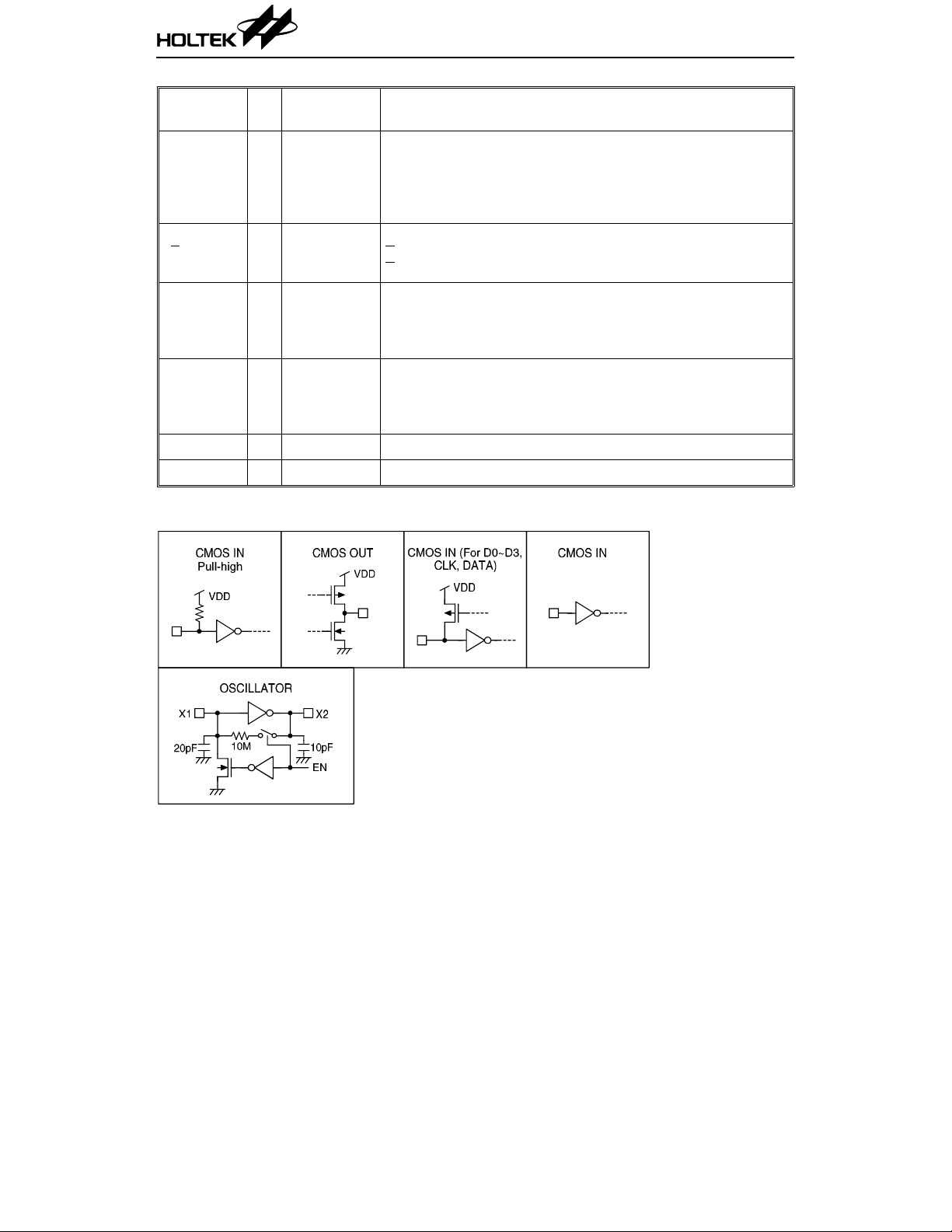
Internal
Connection
CMOS IN
Pull-high
Oscillator
Description
Chip enable, active low
The system oscillator consists of an inverter, a bias resistor, and
the required load capacitor on chip.
The oscillator function can be implemented by Connect a
standard 3.579545MHz crystal to the X1 and X2 terminals.
Pad
No.
Unit: µm
XY
VSS — — Negative power supply
NC — — No connection
2 21st Aug ’98
Page 3
HT9200A/B
Pin Name I/O
D0~D3 I
S/P I CMOS IN
CLK I
DATA I
DTMF O CMOS OUT Output terminal of the DTMF signal
VDD — — Positive power supply, 2.0V~5.5V for normal operation
Approximate internal connection circuits
Internal
Connection
CMOS IN
Pull-high
or floating
CMOS IN
Pull-high
or floating
CMOS IN
Pull-high
or floating
Description
Data inputs for the parallel mode
When the IC is operating in the serial mod e, the data input
terminals (D0~D3) are included with a pull-high resistor. When
the IC is operating in the parallel mode, these pins become
floating.
Operation mode selection input
S/P=“H”: Parallel mode
S/P=“L”: Serial mode
Data synchronous clock input for the serial mode
When the IC is operating in the parallel mode, the input
terminal (CLK) is included with a pull-high res istor. Whe n the
IC is operating in the serial mode, this pin becomes floating.
Data input terminal for the serial mode
When the IC is operating in the parallel mode, the input terminal
(DATA) is included with a pull-high resistor. When the IC is
operating in the serial mode, this pin becomes floating.
3 21st Aug ’98
Page 4

HT9200A/B
Absolu te Maxim um Ratings *
Supply Voltage.................................–0.3V to 6V Storage Temperature.................–50°C to 125°C
Input Voltage.................... V
–0.3 to V
SS
*Note: These are stress ra tings on ly. Stresses exceeding the range specifie d under “Ab solute Maxi -
mum Ratings” ma y cause substantial damage to the device. Functional operation of this
device at other conditions beyond those listed in the specification is not implied and prolonged
exposure to extreme condition s may affect device reliability.
Electrical Cha racteristics Ta=25°C
+0.3V Operating Temperature...............–20°C to 75°C
DD
Symbol Parameter
V
I
DD
V
V
I
STB
R
t
DE
V
I
TOL
V
A
R
t
HD
f
CLK
t
UP
f
OSC
Operating Voltage — — 2 — 5.5 V
DD
Operating Current
“Low” Input Voltage — — VSS — 0.2V
IL
“High” Input Voltage — — 0.8V
IH
Standby Current
Pull-high Resistance
P
DTMF Output Delay
Time (Parallel Mode)
DTMF Output DC
TDC
Level
DTMF Sink Current 2.5V V
DTMF Output AC
TAC
Level
Column Pre-emphasis 2.5V Row group=0dB 1 2 3 dB
CR
DTMF Output Load 2.5V t
L
Tone Signal
Distortion
Clock Input Rate
(Serial Mode)
Oscillator Starting
Time (When
CE is low)
System Frequency — Crystal=3.5795MHz 3.5759 3.5795 3.5831 MHz
Test Conditions
V
DD
2.5V
5.0V — 950 3000
2.5V
5.0V — — 2
2.5V
5.0V 45 68 100
Conditions
S/P=VDD,D0~D3=VSS,
CE=VSS, No load
S/P=VDD,CE=VDD,
No load
VOL=0V
5V — — t
2V~
DTMF Output 0.45V
5.5V
=0.5V –0.1 — — mA
DTMF
2.5V Row group, R
≤ –23dB 5 — — kΩ
HD
2.5V R
=5kΩ —–30–23dB
L
=5kΩ 0.12 0.15 0.18 Vrms
L
Min. Typ. Max. Unit
— 240 2500
DD
—VDDV
DD
—— 1
120 180 270
+6 tUP+8 ms
UP
— 0.75V
DD
DD
— — — 100 500 kHz
The time from
falling edge to normal
5.0V
CE
——10ms
oscillator operation
µA
V
µA
kΩ
V
4 21st Aug ’98
Page 5

Functional Description
The HT9200A/B are DT MF generators for µC
interfaces. They are control led by a
serial mode or the parallel mode (for the
HT9200B only).
Serial mode (HT920 0A/B)
The HT9200A/B employ a data input, a 5-bit
code, and a synchronous clock to transmit a
Table 1: Digits vs. input data vs. tone output frequency (serial mode)
µC in the
Digit D4 D3 D2 D1 D0 Tone Output Frequency (Hz)
100001 697+1209
200010 697+1336
300011 697
400100 770+1209
500101 770+1336
600110 770
700111 852+1209
801000 852+1336
901001 852
001010 941+1336
∗ 010 11 941+1209
# 011 00 941+1477
A01101 697+1633
B01110 770+1633
C01111 852+1633
D00000 941
—10000 697
—10001 770
—10010 852
—10011 941
—10100 1209
—10101 1336
—10110 1477
—10111 1633
DTMF OFF 1 1 1 1 1 —
DTMF signal. Every digit of a phone number to
be transmitted is selected by a s eries of inp uts
which consist of 5-bit data. Of the 5 bi ts, the
D0(LSB) is the first received bit. The
HT9200A/B will latch data on the falling edge of
the clock (CLK pin). T he relationship betwe en
the digital codes and the tone output frequency
is shown in Table 1. As for the control timing
diagram, refer to Figure 1.
+1477
+1477
+1477
+1633
HT9200A/B
*Notes: The codes not listed in Table 1 are not used D4 is MSB
5 21st Aug ’98
Page 6

HT9200A/B
When the system is operating in the serial mode
a pull-high resistor is attached to D0~D3 (for
parallel mode) on the input terminal.
For the HT9200B, the
S/P pin has to be connected
low for serial mode operation.
Parallel mode ( HT9200B)
The HT9200B provides four data inputs D0~D3
to generate their corresponding DTMF signals.
The
S/P has to be connected high to select the
parallel operation mode. Then the input data
codes should be determined. Finally, the
CE is
connected low to transmit the DTMF signal
from the DTMF pin.
The T
time (about 6ms) will be delayed from the
DE
CE falling edge to the DTMF signal output.
The relationship between the digital codes and
the tone output frequency is illustrated in Table 2.
As for the control timing diag ram, see F igure 2.
When the system is operating in the parallel
mode, D0~D3 are all in the floating state. Thus,
these data input pins should not float.
Figure 1
Table 2: Digits vs. input data vs. tone output frequency (parallel mode)
Digit D3 D2 D1 D0 Tone Output Frequency (Hz)
10001 697+1209
20010 697
30011 697
40100 770
50101 770
60110 770
70111 852
81000 852
6 21st Aug ’98
+1336
+1477
+1209
+1336
+1477
+1209
+1336
Page 7

HT9200A/B
Digit D3 D2 D1 D0 Tone Output Frequency (Hz)
91001 852+1477
01010 941
∗ 1011 941+1209
# 1100 941+1477
A1101 697
B1110 770
C1111 852
D0000 941
+1336
+1633
+1633
+1633
+1633
Figure 2
Tone frequency
Output Frequency (Hz)
Specified Actual
697 699 +0.29%
770 766 –0.52%
852 847 –0.59%
941 948 +0.74%
1209 1215 +0.50%
1336 1332 –0.30%
1477 1472 –0.34%
% Error does not contain the crysta l frequency drift
7 21st Aug ’98
%Error
Page 8

Application Circuits
Serial mode
Serial/parallel mode
HT9200A/B
8 21st Aug ’98
 Loading...