Page 1

Features
Operating voltage: 2.5V~5.5V
·
Minimal external components
·
No external filter is required
·
Low standby current (on power down mode)
·
Excellent performance
·
General Description
The HT9170 series are Dual Tone Multi Fre
quency (DTMF) receivers integrated with digi
tal decoder and bandsplit filter functions. The
HT9170B and HT9170D types supply
power-down mode and inhibit mode operations.
All types of the HT9170 series use digital count
ing techniques to detect and decode all the 16
Selection Table
HT9170
DTMF Receiver
Tristate data output for mC interface
·
3.58MHz crystal or ceramic resonator
·
1633Hz can be inhibited by the INH pin
·
HT9170B: 18-pin DIP package
·
HT9170D: 18-pin SOP package
DTMF tone pairs into a 4-bit code output.
-
Highly accurate switched capacitor filters are
employed to divide tone (DTMF) signals into
low and high group signals. A built-in dial tone
rejection circuit is provided to eliminate the
need for pre-filtering.
Function
Part No.
HT9170B 2.5V~5.5V 3.58MHz
HT9170D 2.5V~5.5V 3.58MHz
Operating
Voltage
OSC
Frequency
Tristate
Data Output
ÖÖÖÖ¾
ÖÖÖÖ¾
Power
Down
1633Hz
Inhibit
DV DVB Package
18 DIP
18 SOP
1 December 20, 1999
Page 2

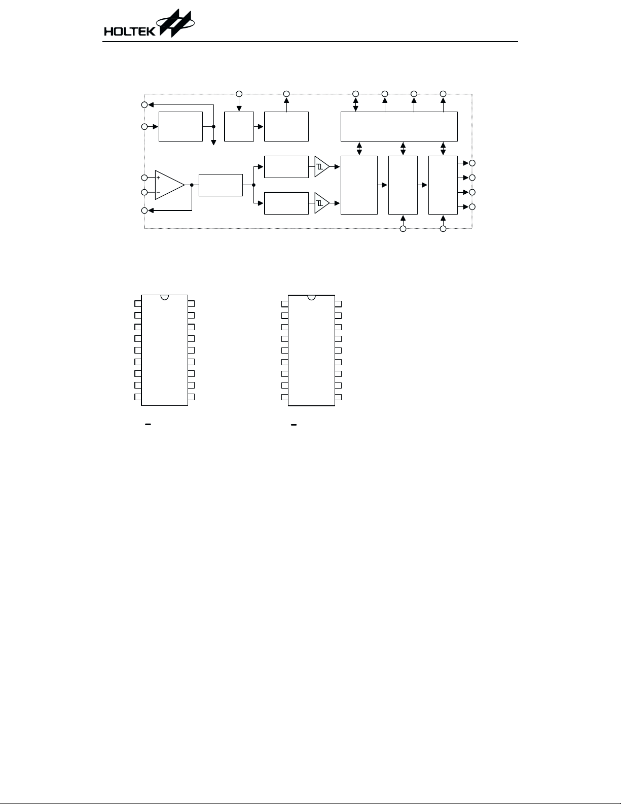
Block Diagram
HT9170
X2
3.58M H z
X1
VP
VN
GS
C rystal
O s c illa to r
OPA
Pin Assignment
VP
VN
GS
VREF
IN H
PW DN
X1
X2
VSS
1
2
3
4
5
6
7
8
9
H T 9170B
18
17
16
15
14
13
12
11
10
1 8 D IP
Pre -Filter
VDD
RT/GT
EST
DV
D3
D2
D1
D0
OE
PW DN DVB
Bias
Circuit
VREF RT/GT EST DV
Low G roup
H igh G roup
VP
VN
GS
VREF
IN H
PW DN
X1
X2
VSS
Vref
G enerator
F ilte r
Filter
1
2
3
4
5
6
7
8
9
18
17
16
15
14
13
12
11
10
Steering C ontrol C ircuit
Frequency
Detector
VDD
RT/GT
EST
DV
D3
D2
D1
D0
OE
C ode
Detector
IN H
Latch
&
Output
Buffer
OE
H T 9170D
1 8 S O P
D0
D1
D2
D3
2 December 20, 1999
Page 3

Pin Description
HT9170
Pin Name I/O
VP I
VN I Operational amplifier inverting input
GS O Operational amplifier output terminal
VREF O VREF Reference voltage output, normally V
X1 I
X2 O
PWDN I
INH I
VSS
OE I
D0~D3 O
DV O CMOS OUT
EST O CMOS OUT Early steering output (see Functional Description)
RT/GT I/O CMOS IN/OUT
VDD
DVB O CMOS OUT
¾¾
¾¾
Internal
Connection
OPERATIONAL
AMPLIFIER
OSCILLATOR
CMOS IN
Pull-low
CMOS IN
Pull-low
CMOS IN
Pull-high
CMOS OUT
Tristate
Description
Operational amplifier non-inverting input
/2
DD
The system oscillator consists of an inverter, a bias resistor
and the necessary load capacitor on chip.
A standard 3.579545MHz crystal connected to X1 and X2 ter
minals implements the oscillator function.
Active high. This enables the device to go into power down
mode and inhibits the oscillator. This pin input is internally
pulled down.
Logic high. This inhibits the detection of tones representing
characters A, B, C and D. This pin input is internally pulled
down.
Negative power supply
D0~D3 output enable, high active
Receiving data output terminals
OE=²H²: Output enable
OE=²L²: High impedance
Data valid output
When the chip receives a valid tone (DTMF) signal, the DV
goes high; otherwise it remains low.
Tone acquisition time and release time can be set through
connection with external resistor and capacitor.
Positive power supply, 2.5V~5.5V for normal operation
One-shot type data valid output, normal high, when the chip
receives a valid time (DTMF) signal, the DVB goes low for
10ms.
-
3 December 20, 1999
Page 4

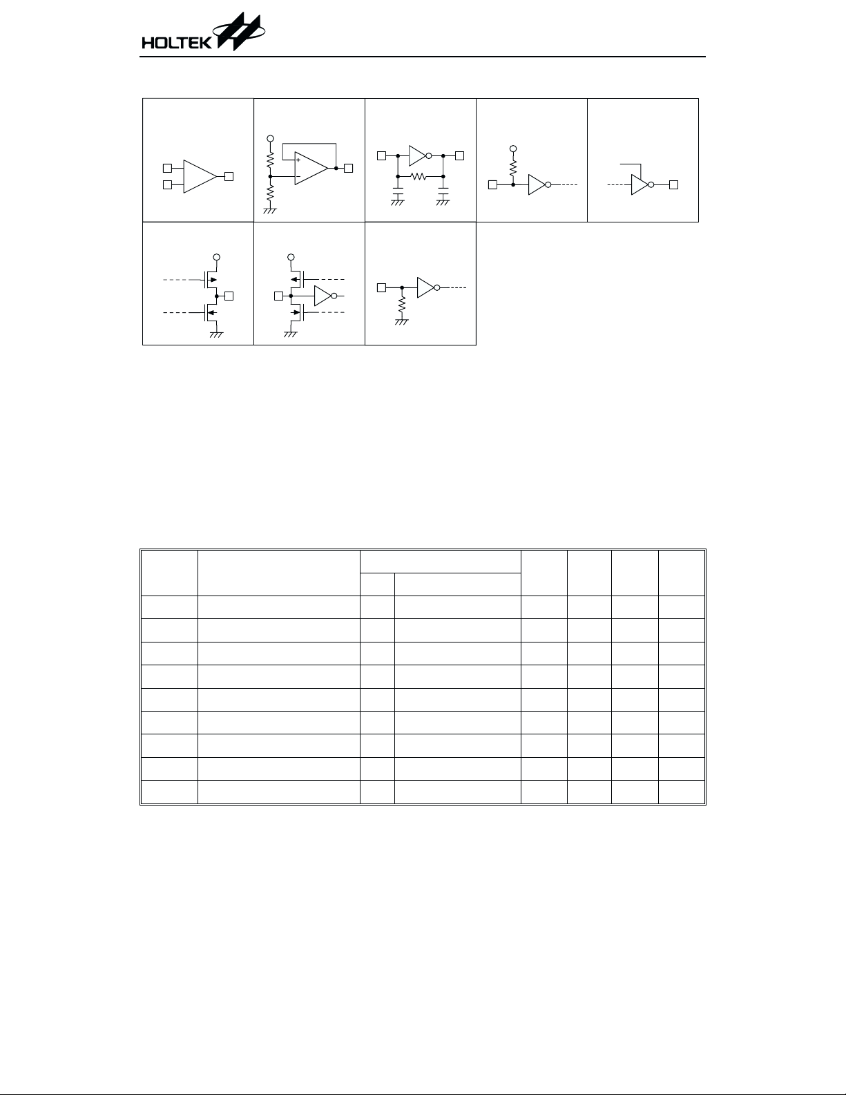
Approximate internal connection circuits
HT9170
OPERATION AL
AM PLIFIER
V-
VN
OPA
V+
VP
CMOS OUT
GS
VREF
OPA
CMOS IN/OUT
O SC ILLA TO R
X1
20pF
CMOS IN
Pull-low
10M
X2
10pF
CMOS IN
Pull-high
CMOS OUT
Tristate
EN
Absolute Maximum Ratings
Supply Voltage.................................-0.3V to 6V
Input Voltage .................V
-0.3V to VDD+0.3V
SS
Note: These are stress ratings only. Stresses exceeding the range specified under ²Absolute Maxi
mum Ratings² may cause substantial damage to the device. Functional operation of this device
at other conditions beyond those listed in the specification is not implied and prolonged exposure to extreme conditions may affect device reliability.
Storage Temperature.................-50°Cto125°C
Operating Temperature ..............-20°Cto75°C
-
D.C. Characteristics
Symbol Parameter
V
I
I
V
V
I
I
R
R
DD
STB
IL
IH
Operating Voltage
DD
Operating Current 5V
Standby Current 5V PWDN=5V
²Low² Input Voltage
IL
²High² Input Voltage
IH
²Low² Input Current
²High² Input Current
Pull-high Resistance (OE) 5V
OE
Input Impedance (VN, VP) 5V
IN
Test Conditions
V
DD
Conditions
¾¾
¾¾
5V
5V
5V
5V
V
VP=VVN
V
VP=VVN
V
OE
¾¾¾
¾
=0V
=5V
=0V
¾¾10¾ MW
4 December 20, 1999
Ta=25°C
Min. Typ. Max. Unit
2.5 5 5.5 V
3.0 7 mA
¾
10 25
mA
1.0 V
4.0
¾¾
¾¾
¾¾
0.1
0.1
60 100 150
V
mA
mA
kW
Page 5

HT9170
Symbol Parameter
I
I
f
OH
OL
OSC
Source Current
(D0~D3, EST, DV)
Sink Current
(D0~D3, EST, DV)
System Frequency 5V Crystal=3.5795MHz 3.5759 3.5795 3.5831 MHz
A.C. Characteristics
Symbol Parameter
DTMF Signal
Input Signal Level
Twist Accept Limit (Positive) 5V
Twist Accept Limit (Negative) 5V
Dial Tone Tolerance 5V
Noise Tolerance 5V
Third Tone Tolerance 5V
Frequency Deviation
Acceptance
Frequency Deviation Rejection 5V
Power Up Time (t
(See Figure 4.)
Gain Setting Amplifier
R
I
IN
V
P
C
A
f
T
V
Input Resistance 5V
IN
Input Leakage Current 5V
Offset Voltage 5V
OS
Power Supply Rejection 5V
SRR
Common Mode Rejection 5V
MRR
Open Loop Gain 5V
VO
Gain Band Width 5V
Output Voltage Swing 5V
OUT
PU
Test Conditions
Min. Typ. Max. Unit
V
DD
5V
5V
Conditions
=4.5V
V
OUT
=0.5V
V
OUT
-0.4 -0.8 ¾
1.0 2.5
f
=3.5795MHz, Ta=25°C
OSC
¾
mA
mA
Test Conditions
Min. Typ. Max. Unit
V
DD
3V
Conditions
-36 ¾-6
dBm
5V
-29 ¾
10
¾
10
¾
18
¾
¾-12 ¾
¾-16 ¾
5V
¾¾±1.5
±3.5 ¾¾
)
5V
¾
30
¾
¾
¾
¾
1
dB
dB
dB
dB
dB
%
%
ms
¾¾10¾ MW
V
<(VVP,VVN)<V
SS
DD
¾¾±25 ¾
100 Hz
IN
<3V
-3V<V
¾¾
>100kW¾
R
L
¾
¾
¾
¾
0.1
60
60
65
1.5
4.5
¾mA
mV
dB
¾
dB
¾
dB
¾
MHz
¾
V
¾
PP
5 December 20, 1999
Page 6

HT9170
Symbol Parameter
R
C
V
Load Resistance (GS) 5V
L
Load Capacitance (GS) 5V
L
Common Mode Range 5V No load
CM
Steering Control
t
DP
t
DA
t
ACC
t
REJ
t
IA
t
IR
t
PDO
t
PDV
t
DOV
t
DDO
t
EDO
Tone Present Detection Time 5 16 22 ms
Tone Absent Detection Time
Acceptable Tone Duration
Rejected Tone Duration 20
Acceptable Inter-digit Pause
Rejected Inter-digit Pause 20
Propagation Delay
(RT/GT to DO)
Propagation Delay
(RT/GT to DV)
Output Data Set Up (DO to DV)
Disable Delay (OE to DO)
Enable Delay (OE to DO)
Test Conditions
V
DD
Conditions
Min. Typ. Max. Unit
¾¾50¾ kW
¾
¾
100
3.0
4 8.5 ms
¾¾
¾¾
¾¾
¾¾
¾¾
¾
¾
¾
¾
¾
811
12
4.5
300
50 60 ns
pF
¾
V
¾
42 ms
ms
42 ms
ms
ms
¾ms
¾ms
ns
¾
PP
Note: DO=D0~D3
Tone
100k
0.1mF
3.579545M H z
100k
VSS
1
2
3
4
W
5
6
7
8
9
HT9170/B/D
W
20pF20pF
VP
VN
GS
VREF
(IN H )
(P W D N )
X1
X2
VSS
VDD
RT/G T
EST
Figure 1. Test circuit
6 December 20, 1999
DV
D3
D2
D1
D0
OE
V
DD
0.1mF
18
17
16
15
300k
W
14
13
12
11
10
Page 7

Functional Description
HT9170
Overview
The HT9170 series tone decoders consist of
three band pass filters and two digital decode
circuits to convert a tone (DTMF) signal into
digital code output.
An operational amplifier is built-in to adjust
the input signal (refer to Figure 2).
C
V
i
R1
RF
VP
VN
GS
VREF
H T 9170
Series
(a) S tandard input circuit
C
V
i1
V
i2
R1
R2
C
R4R3
R5
VP
VN
GS
VREF
H T 9170
Series
(b ) D iffe re n tia l in p u t c irc u it
Figure 2. Input operation for amplifier applica-
tion circuits
The pre-filter is a band rejection filter which reduces the dialing tone from 350Hz to 400Hz.
The low group filter filters low group frequency
signal output whereas the high group filter fil
ters high group frequency signal output.
Each filter output is followed by a zero-crossing
detector with hysteresis. When each signal am
plitude at the output exceeds the specified
level, it is transferred to full swing logic signal.
When input signals are recognized to be effec
tive, DV becomes high, and the correct tone
code (DTMF) digit is transferred.
Steering control circuit
The steering control circuit is used for measur
ing the effective signal duration and for protect
ing against drop out of valid signals. It employs
the analog delay by external RC time-constant
controlled by EST.
The timing is shown in Figure 3. The EST pin is
normally low and draws the RT/GT pin to keep
low through discharge of external RC. When a
valid tone input is detected, EST goes high to
charge RT/GT through RC.
When the voltage of RT/GT changes from 0 to
V
(2.35V for 5V supply), the input signal is
TRT
effective, and the correct code will be created by
the code detector. After D0~D3 are completely
latched, DV output becomes high. When the
voltage of RT/GT falls down from VDD to V
(i.e.., when there is no input tone), DV output
becomes low, and D0~D3 keeps data until a
next valid tone input is produced.
By selecting adequate external RC value, the min
imum acceptable input tone duration (t
the minimum acceptable inter-tone rejection (t
can be set. External components (R, C) are chosen
by the formula (refer to Figure 5.):
-
t
ACC=tDP+tGTP
t
IR=tDA+tGTA
where t
;
;
: Tone duration acceptable time
ACC
: EST output delay time (²L²®²H²)
t
DP
t
: Tone present time
GTP
t
: Inter-digit pause rejection time
IR
: EST output delay time (²H²®²L²)
t
DA
t
: Tone absent time
GTA
-
-
ACC
TRT
) and
IR
-
-
-
)
7 December 20, 1999
Page 8

Timing Diagrams
HT9170
Tone
EST
RT/GT
D0~D3
DV
OE
Tone
t
REJ
t
IA
t
IR
Tone n Tone n+1
t
t
t
DP
V
TRT
DP
t
ACC
t
PDO
t
DA
Tone C ode n 1 Tone C ode n
t
DOV
t
PDV
DP
t
DDO
t
GTP
t
PDV
t
GTA
Tone C ode n+1
t
EDO
Figure 3. Steering timing
Tone
PW DN
EST
t
PU
Figure 4. Power up timing
8 December 20, 1999
Page 9

HT9170
V
V
DD
DD
H T 9170
VDD
Series
RT/G T
EST
(a) Fundamental circuit:
=R´ C ´ Ln (VDD/(V
t
GTP
=R´ C ´ Ln (VDD/V
t
GTA
H T 9170
VDD
Series
RT/GT
EST
(b) t
GTP<tGTA
t
GTP
t
GTA
:
= (R1 // R2) ´ C ´ Ln (V
=R1´ C ´ Ln (VDD/V
DTMF dialing matrix
C O L1 C O L2 C O L3 CO L4
1
2
ROW 1
ROW 2
ROW 3
ROW 4
4
7
*
3
5
6
8
9
0
#
H T 9170
D1
R
DD -VTRT
)
TRT
R1
R2
DD -VTRT
TRT
C
))
V
DD
C
(c) t
))
)
Series
GTP>tGTA
=R1´ C ´ Ln (VDD/(VDD- V
t
GTP
= (R1 // R2) ´ C ´ Ln (VDD/V
t
GTA
Figure 5. Steering time adjustment circuits
A
B
C
D
RT/G T
:
VDD
EST
D1
R1
R2
TRT
TRT
C
))
)
9 December 20, 1999
Page 10

HT9170
DTMF data output table
Low Group (Hz) High Group (Hz) Digit OE D3 D2 D1 D0
697 1209 1 H L L L H
697 1336 2 H L L H L
697 1477 3 H L L H H
770 1209 4 H L H L L
770 1336 5 H L H L H
770 1477 6 H L H H L
852 1209 7 H L H H H
852 1336 8 H H L L L
852 1477 9 H H L L H
941 1336 0 H H L H L
941 1209 * H H L H H
941 1477 # H H H L L
697 1633 A H H H L H
770 1633 B HHHH L
852 1633 C HHHHH
941 1633 D H L L L L
¾¾
ANYLZZZZ
Z: High impedance
Data output
The data outputs (D0~D3) are tristate outputs. When OE input becomes low, the data outputs
(D0~D3) are high impedance.
10 December 20, 1999
Page 11

Application Circuits
DTM F
100k
0.1mF
To other device
X'TAL
C1
100k
VSS
1
2
3
4
W
5
6
7
8
9
H T 9170B /D
W
C2
VP
VN
GS
VREF
IN H
PW DN
X1
X2
VSS
VDD
RT/GT
EST
18 D IP /S O P
N ote: (a) X 'TA L = 3.579545M H z crystal
C 1 = C 2 @ 20pF
(b ) X 'T A L = 3 .5 8 M H z c e ra m ic re s o n a to r
C 1 = C 2 @ 39pF
DV
D3
D2
D1
D0
OE
V
18
17
16
15
14
13
12
11
10
DD
0.1mF
300k
W
To other device
HT9170
11 December 20, 1999
Page 12

HT9170
Holtek Semiconductor Inc. (Headquarters)
No.3 Creation Rd. II, Science-based Industrial Park, Hsinchu, Taiwan, R.O.C.
Tel: 886-3-563-1999
Fax: 886-3-563-1189
Holtek Semiconductor Inc. (Taipei Office)
5F, No.576, Sec.7 Chung Hsiao E. Rd., Taipei, Taiwan, R.O.C.
Tel: 886-2-2782-9635
Fax: 886-2-2782-9636
Fax: 886-2-2782-7128 (International sales hotline)
Holtek Semiconductor (Hong Kong) Ltd.
RM.711, Tower 2, Cheung Sha Wan Plaza, 833 Cheung Sha Wan Rd., Kowloon, Hong Kong
Tel: 852-2-745-8288
Fax: 852-2-742-8657
Copyright Ó 1999 by HOLTEK SEMICONDUCTOR INC.
The information appearing in this Data Sheet is believed to be accurate at the time of publication. However, Holtek
assumes no responsibility arising from the use of the specifications described. The applications mentioned herein are
used solely for the purpose of illustration and Holtek makes no warranty or representation that such applications
will be suitable without further modification, nor recommends the use of its products for application that may pres
ent a risk to human life due to malfunction or otherwise. Holtek reserves the right to alter its products without prior
notification. For the most up-to-date information, please visit our web site at http://www.holtek.com.tw.
12 December 20, 1999
-
 Loading...